

Page 1
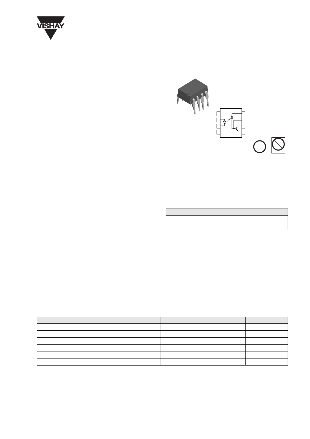
SFH6135/ SFH6136
i179081
1
2
3
4
8
7
6
5
C(VCC)
NC
A
C
NC
B(V
B
)
C(V
O
)
E (GND)
Vishay Semiconductors
High Speed Optocoupler, 1 MBd, Transistor Output
Features
• Isolation Test Voltage: 5300 V
• TTL Compatible
• High Bit Rates: 1.0 Mbit/s
• High Common-mode Interference Immunity
• Bandwidth 2.0 MHz
• Open-collector Output
• External Base Wiring Possible
• Lead-free component
• Component in accordance to RoHS 2002/95/EC
and WEEE 2002/96/EC
RMS
e3
Pb
Pb-free
Agency Approvals
• UL1577, File No. E52744 System Code H or J,
Double Protection
• CSA 93751
• DIN EN 60747-5-2 (VDE0884)
Signals can be transmitted between two electrically
separated circuits up to frequencies of 2.0 MHz. The
potential difference between the circuits to be coupled
should not exceed the maximum permissible reference voltages.
DIN EN 60747-5-5 pending
Available with Option 1
Description
The SFH6135 and SFH6136 optocouplers feature a
high signal transmission rate and a high isolation
resistance. They have a GaAIAs infrared emitting
Order Information
Part Remarks
SFH6135 CTR ≥ 7.0 %, DIP-8
SFH6136 CTR ≥ 19 %, DIP-8
For additional information on the available options refer to
Option Information.
diode, optically coupled with an integrated photo
detector which consists of a photo diode and a highspeed transistor in a DIP-8 plastic package.
Absolute Maximum Ratings
T
= 25 °C, unless otherwise specified
amb
Stresses in excess of the absolute Maximum Ratings can cause permanent damage to the device. Functional operation of the device is
not implied at these or any other conditions in excess of those given in the operational sections of this document. Exposure to absolute
Maximum Rating for extended periods of the time can adversely affect reliability.
Input
Parameter Test condition Symbol Val ue Unit
Reverse voltage V
Forward current I
Peak forward current t = 1.0 ms, duty cycle 50 % I
Maximum surge forward current t ≤ 1.0 µs, 300 pulses/s I
Thermal resistance R
Power dissipation P
R
F
FM
FSM
thja
diss
3.0 V
25 mA
50 mA
1.0 A
700 K/W
45 mW
Document Number 83668
Rev. 1.5, 26-Oct-04
www.vishay.com
1
Page 2
SFH6135/ SFH6136
VISHAY
Vishay Semiconductors
Output
Parameter Test condition Symbol Va lue Unit
Supply voltage V
Output voltage V
Emitter-base voltage V
Output current I
Maximum output current I
Base current I
Thermal resistance R
Power dissipation T
= 70 °C P
amb
S
O
EBO
O
O
B
thja
diss
- 0.5 to 30 V
- 0.5 to 25 V
5.0 V
8.0 mA
16 mA
5.0 mA
300 K/W
100 mW
Coupler
Parameter Test condition Symbol Va lue Unit
Isolation test voltage V
ISO
Pollution degree (DIN VDE
0110)
Creepage ≥ 7.0 mm
Clearance ≥ 7.0 mm
Comparative tracking index per
DIN IEC 112/VDE 0303 part 1
Isolation resistance V
= 500 V, T
IO
V
= 500 V, T
IO
Storage temperature range T
Ambient temperature range T
Soldering temperature max. ≤10 s, dip soldering
= 25 °C R
amb
= 100 °C R
amb
T
IO
IO
stg
amb
sld
≥ 0.5 mm distance from case
bottom
5300 V
2
175
12
≥ 10
11
≥ 10
- 55 to + 125 °C
- 55 to + 100 °C
260 °C
RMS
Ω
Ω
Electrical Characteristics
T
= 25 °C, unless otherwise specified
amb
Minimum and maximum values are testing requirements. Typical values are characteristics of the device and are the result of engineering
evaluation. Typical values are for information only and are not part of the testing requirements.
Input
Parameter Test condition Symbol Min Ty p. Max Unit
Forward voltage I
Breakdown voltage I
Reverse current V
Capacitance V
Temperature coefficient of
forward voltage
www.vishay.com
2
= 16 mA V
F
= 10 µAV
R
= 3.0 V I
R
= 0 V, f = 1.0 MHz C
R
I
= 16 mA ∆VF/∆T
F
BR
R
F
3.0 V
O
amb
1.6 1.9 V
0.5 10 µA
125 pF
1.7 mV/°C
Document Number 83668
Rev. 1.5, 26-Oct-04
Page 3
VISHAY
Output
Parameter Test condition Part Symbol Min Ty p. Max Unit
Logic low supply current I
Logic high supply current I
Output voltage, output low I
Output current, output high I
Coupler
Parameter Test condition Symbol Min Ty p . Max Unit
Capacitance (input-output) f = 1.0 MHz C
Current Transfer Ratio
Parameter Test condition Part Symbol Min Ty p. Max Unit
Current Transfer Ratio I
= 16 mA, VO open, VCC = 15 V I
F
= 0 mA, VO open, VCC = 15 V I
F
= 16 mA, VCC = 4.5 V,
F
= 1.1 mA
I
O
I
= 16 mA, VCC = 4.5 V,
F
= 2.4 mA
I
O
= 0 mA, VO = VCC = 5.5 V I
F
I
= 0 mA, VO = VCC = 15 V I
F
= 16 mA, VO = 0.4 V,
F
= 4.5 V
V
CC
SFH6135 V
SFH6136 V
SFH6135 CTR 7 16 %
SFH6136 CTR 19 35 %
= 16 mA, VO = 0.5 V,
I
F
V
= 4.5 V
CC
SFH6135 CTR 5 %
SFH6136 CTR 15 %
SFH6135/ SFH6136
Vishay Semiconductors
CCL
CCH
OL
OL
OH
OH
IO
150 µA
0.01 1.0 µA
0.1 0.4 V
0.1 0.4 V
3.0 500 nA
0.01 1.0 µA
0.6 pF
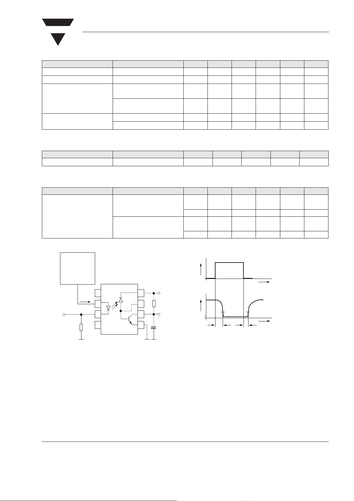
isfh6135_01
Pulse generator
Z
=50Ω
O
t
tf=5ns
,
r
duty cycle 10%
t≤100 µs
I
F
I
Monitor
F
100
I
F
t
R
L
C
15 pF
5V
V
L
V
O
O
V
OL
t
PHL
t
PLH
5V
1.5 V
t
1
2
3
4
Ω
ı
8
7
6
5
Figure 1. Schematics
Document Number 83668
Rev. 1.5, 26-Oct-04
www.vishay.com
3
Page 4

SFH6135/ SFH6136
Vishay Semiconductors
Switching Characteristics
Delay Time
Parameter Test condition Part Symbol Min Ty p. Max Unit
High-low I
Low-high I
I
1
F
2
A
isfh6135_02
B
V
FF
3
4
Pulse generator
+V
CM
Z
t
O
,
tf=8ns
r
= 16 mA, VCC = 5.0 V,
F
= 4.1 kΩ
R
L
I
= 16 mA, VCC = 5.0 V,
F
= 1.9 kΩ
R
L
= 16 mA, VCC = 5.0 V,
F
= 4.1 kΩ
R
L
I
= 16 mA, VCC = 5.0 V,
F
= 1.9 kΩ
R
L
8
7
6
5
=50Ω
VISHAY
SFH6135 t
SFH6136 t
SFH6135 t
SFH6136 t
V
CM
5V
R
L
V
O
V
V
PHL
PHL
PLH
PLH
10 V
90%
10% 90%
0V
t
O
5V
O
V
r
OL
t
f
10%
0.3 1.5 µs
0.2 0.8 µs
0.3 1.5 µs
0.2 0.8 µs
t
=0mA
A: I
F
t
=16mA
B: I
F
t
Figure 2. Common-Mode Interference Immunity
Common Mode Transient Immunity
Parameter Test condition Part Symbol Min Ty p. Max Unit
High V
Low V
= 10 V
CM
= 0 mA, RL = 4.1 kΩ
I
F
V
= 10 V
CM
I
= 0 mA, RL = 1.9 kΩ
F
= 10 V
CM
= 0 mA, RL = 4.1 kΩ
I
F
V
= 10 V
CM
I
= 0 mA, RL = 1.9 kΩ
F
, VCC = 5.0 V,
P-P
, VCC = 5.0 V,
P-P
, VCC = 5.0 V,
P-P
, VCC = 5.0 V,
P-P
SFH6135 CM
SFH6136 CM
SFH6135 CM
SFH6136 CM
H
H
L
L
1000 V/µs
1000 V/µs
1000 V/µs
1000 V/µs
www.vishay.com
4
Document Number 83668
Rev. 1.5, 26-Oct-04
Page 5

VISHAY
isfh6135_06
25
20
15
10
5
0
0 5 10 15 20 25
Output Voltage, Vo (V)
Output Current, Io(mA)
IF=15mA
IF=10mA
IF=5mA
IF=40mA
IF=20mA
IF=35mA
IF=30mA
IF=25mA
(VCC= 5.0 V)
isfh6135_07
8
7
6
5
4
3
2
1
0
-60 -40 -20 0 20 40 60 80 100
Output Current, Io (mA)
Temperature, Ta (°C)
IF = 20mA
IF = 16mA
IF = 10mA
IF=2mA
IF=1mA
@VO= 0.4 V, VCC= 5.0
isfh6135_08
900
800
700
600
500
400
300
200
100
0
-60 -40 -20 0 20 40 60 80 100
tp - Propagation Delay Time - ns
Temperature, Ta (°C)
TpLH @ 3 V
TpHL@3V
TpHL @ 1.5 V
TpLH @ 1.5 V
SFH6136 @ VCC= 5.0 V
IF= 16 mA, RL= 1.9 kΩ
SFH6135/ SFH6136
Vishay Semiconductors
Typical Characteristics (Tamb = 25 °C unless otherwise specified)
20
15
75 °C
- LED Current in mA
F
I
10
5
25 °C
0°C
0
VF- LED forward Voltage
isfh6135_03
1.71.61.51.41.3
Figure 3. LED Forward Current vs.Forward Voltage
30
20
LED Current in ma
F
10
I
isfh6135_04
0
Ambient Temperature in °C
100806040200
Figure 4. Permissible Forward LED Current vs. Temperature
Figure 6. Output Current vs. Output Voltage
Figure 7. Output Current vs. Temperature
120
100
80
60
40
Total Power in mW
20
0
isfh6135_05
Figure 5. Permissible Power Dissipation vs. Temperature
Document Number 83668
Rev. 1.5, 26-Oct-04
Detector
Emitter
Ambient Temperature in °C
100806040200
Figure 8. Propagation Delay vs. Temperature-SFH6136
www.vishay.com
5
Page 6

SFH6135/ SFH6136
Vishay Semiconductors
1400
SFH1635 @ VCC= 5.0 V,
1200
IF=16mA,RL= 4.1 kΩ
1000
800
600
400
200
tp - Propagation Delay Time - ns
0
-60 -40 -20 100
isfh6135_09
Figure 9. Propagation Delay vs. Temperature-SFH6135
100
10
VCC=VO=15V
1
TpLH
TpHL
0
20 40
Temperature, Ta (°C)
60
VCC=VO=5V
VISHAY
80
0.1
0.01
- Collector Current, IC (nA)
OH
I
0.001
-60 -40 -20 100
isfh6135_10
0
20
Temperature, TA(°C)
40
60 80
Figure 10. Logic High Output Current vs.Temperature
/ Small Signal Current
O
/∆i
F
ˇ
∆i
isfh6135_11
0.6
0.5
0.4
0.3
0.2
Transfer Ratio
0.1
0
0
5
(VCC= 5.0 V, RL= 100 Ω)
10 15 20 25
IF/mA
Figure 11. Small Signal Current Transfer Ratio vs. Quiescent Input
Current
www.vishay.com
6
Document Number 83668
Rev. 1.5, 26-Oct-04
Page 7

VISHAY
Package Dimensions in Inches (mm)
pin one ID
SFH6135/ SFH6136
Vishay Semiconductors
i178006
.255 (6.48)
.268 (6.81)
.030 (0.76)
.045 (1.14)
4° typ.
.050 (1.27)
.018 (.46)
.022 (.56)
4
3
5
6
.379 (9.63)
.390 (9.91)
.100 (2.54) typ.
1
2
78
.031 (0.79)
.130 (3.30)
.150 (3.81)
.020 (.51 )
.035 (.89 )
ISO Method A
.300 (7.62)
typ.
10°
3°–9°
.008 (.20)
.012 (.30)
.110 (2.79)
.130 (3.30)
.230(5.84)
.250(6.35)
Document Number 83668
Rev. 1.5, 26-Oct-04
www.vishay.com
7
Page 8

SFH6135/ SFH6136
VISHAY
Vishay Semiconductors
Ozone Depleting Substances Policy Statement
It is the policy of Vishay Semiconductor GmbH to
1. Meet all present and future national and international statutory requirements.
2. Regularly and continuously improve the performance of our products, processes, distribution and
operatingsystems with respect to their impact on the health and safety of our employees and the public, as
well as their impact on the environment.
It is particular concern to control or eliminate releases of those substances into the atmosphere which are
known as ozone depleting substances (ODSs).
The Montreal Protocol (1987) and its London Amendments (1990) intend to severely restrict the use of ODSs
and forbid their use within the next ten years. Various national and international initiatives are pressing for an
earlier ban on these substances.
Vishay Semiconductor GmbH has been able to use its policy of continuous improvements to eliminate the use
of ODSs listed in the following documents.
1. Annex A, B and list of transitional substances of the Montreal Protocol and the London Amendments
respectively
2. Class I and II ozone depleting substances in the Clean Air Act Amendments of 1990 by the Environmental
Protection Agency (EPA) in the USA
3. Council Decision 88/540/EEC and 91/690/EEC Annex A, B and C (transitional substances) respectively.
Vishay Semiconductor GmbH can certify that our semiconductors are not manufactured with ozone depleting
substances and do not contain such substances.
We reserve the right to make changes to improve technical design
and may do so without further notice.
Parameters can vary in different applications. All operating parameters must be validated for each
customer application by the customer. Should the buyer use Vishay Semiconductors products for any
unintended or unauthorized application, the buyer shall indemnify Vishay Semiconductors against all
claims, costs, damages, and expenses, arising out of, directly or indirectly, any claim of personal
damage, injury or death associated with such unintended or unauthorized use.
Vishay Semiconductor GmbH, P.O.B. 3535, D-74025 Heilbronn, Germany
Telephone: 49 (0)7131 67 2831, Fax number: 49 (0)7131 67 2423
www.vishay.com
8
Document Number 83668
Rev. 1.5, 26-Oct-04
Page 9

Legal Disclaimer Notice
Vishay
Document Number: 91000 www.vishay.com
Revision: 08-Apr-05 1
Notice
Specifications of the products displayed herein are subject to change without notice. Vishay Intertechnology, Inc.,
or anyone on its behalf, assumes no responsibility or liability for any errors or inaccuracies.
Information contained herein is intended to provide a product description only. No license, express or implied, by
estoppel or otherwise, to any intellectual property rights is granted by this document. Except as provided in Vishay's
terms and conditions of sale for such products, Vishay assumes no liability whatsoever, and disclaims any express
or implied warranty, relating to sale and/or use of Vishay products including liability or warranties relating to fitness
for a particular purpose, merchantability, or infringement of any patent, copyright, or other intellectual property right.
The products shown herein are not designed for use in medical, life-saving, or life-sustaining applications.
Customers using or selling these products for use in such applications do so at their own risk and agree to fully
indemnify Vishay for any damages resulting from such improper use or sale.
 Loading...