

Page 1
Application Note
Vishay General Semiconductor
Design Guidelines for Schottky Rectifiers
Known limitations of Schottky rectifiers
- including limited high temperature operation, high leakage and limited voltage range -
can be measured and controlled, allowing wide application on switch mode power supplies.
By Jon Schleisner, Senior Technical Marketing Manager
Schottky rectifiers have been used in the power supply
industry for approximately 15 years. During this time,
significant fiction as well as fact has been associated with
this type of rectifier. The primary assets of Schottky devices
are switching speeds approaching zero-time and very low
forward voltage drop (V
). This combination makes Schottky
F
barrier rectifiers ideal for the output stages of switching
power supplies. On the negative side, Schottky devices are
also known for limited high-temperature operation, high
leakage and limited voltage range B
. Though these
VR
limitations exist, they are quantifiable and controllable,
allowing wide application of these devices in switch mode
power supplies.
High leakage, when associated with standard P-N junction
rectifiers, usually indicates “badness,” implying poor
reliability. In a Schottky device, leakage at high temperature
(75 °C and greater) is often on the order to several milliamps,
depending on chip size. In the case of Schottky barrier
rectifiers, high-temperature leakage and forward voltage
drop are controlled by two primary factors: the size of the
chip’s active area and the barrier height (φB).
Design of a Schottky rectifier can be viewed as a tradeoff. A
high barrier height device exhibits low leakage at high
temperature, however, the forward voltage drop increases.
These parameters are also controlled by the die size and
resistivity of the starting material. A larger die will lower the
VF but raise the leakage if all other parameters are held
constant. The resistivity of the starting material must be
chosen in a range where the breakdown voltage (B
) is not
VR
degraded at the low end and the forward end of the resistivity
range. Since a larger chip size is obviously more expensive,
this is not the primary method for controlling these
parameters. Chip size is usually set to a dimension where the
current density through the die is kept at a safe level.
BARRIER HEIGHT (φB), A FACTOR
Vishay General Semiconductor produces two product lines
of Schottky barrier rectifiers. One line is referred to as the
“MBR” series, a high-temperature, low-leakage, relatively
high VF type of Schottky device with a high barrier height
(φB). The second line is the “SBL” series, designed to
operate at lower temperature (125 °C or less); however,
while leakage current is higher, forward voltage drop (V
significantly lower and they are designed with a low-φB
barrier height. The low- φB-line SBL series uses a nichrome
barrier metal with a barrier height of φB = 0.64 eV. The
high-φB MBR series uses a nichrome-platinum barrier metal
www.vishay.com For technical questions within your region, please contact: Document Number: 88840
1468 PDD-Americas@vishay.com
) is
F
, PDD-Asia@vishay.com, PDD-Europe@vishay.com Revision: 26-Aug-08
to achieve barrier height (φB = 0.71 eV). Both series are
guard-ring protected against excessive transient voltages.
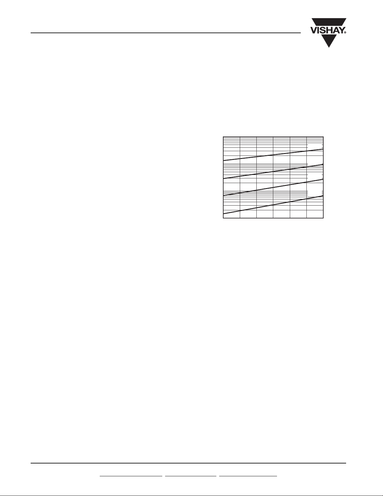
1
150 °C
125 °C
100 °C
75 °C
2
A/cm
0.001
0.1
0.01
02010
4030 6050
Voltage (V)
Figure 1.
Both the low and high-barrier-height Schottky devices are
valuable in a variety of applications.When the true operating
temperature of the Schottky rectifier exceeds 125 °C, the
high-barrier-height series must be used to avoid thermal
runaway.
This occurs when excessive self-heating of the rectifier
causes large leakage currents, resulting in additional
selfheating. The process becomes a form of positive thermal
feedback and may lead to damage in the rectifier or
inappropriate functioning of the circuit utilizing the device.
Using a high-barrier-height (MBR) component prevents this
anomaly, but sacrifices higher forward voltage. Operating the
low barrier height (SBL) series at a junction temperature of
125 °C, a decision on the use of a low- or high-barrier-height
Schottky device must be made.
The following procedure has been developed to provide an
analytical method of selecting the most efficient Schottky
barrier device for a given application.
Page 2
CALCULATING THE BARRIER HEIGHT (φB)
OF SCHOTTKY RECTIFIERS
Calculating the barrier height of a Schottky rectifier where φB
is not given is a straightforward process. The following two
equations will yield an excellent engineering approximation
of the barrier height, φB:
φ
B = (- KT/q) LN (J/R x T) (1)
= I0 /ACTIVE AREA (cm2)
J
0
φ
B = barrier height (eV)
K = Boltzmann’s constant = 8.62 x 10⁵ eV/°K
T = ambient temperature in degrees kelvin
= current density at zero volts
J
0
R* = Richardon’s constant = 112/cm
I0 = forward current at zero volts
To solve Equation One, the current density J
Two) must be found first:
2k2
(Equation
0
Application Note
Vishay General Semiconductor
10 000
(µA)
I
I0 point
This result is then placed into the first equation:
J0 = I0/active area (cm2) (2)
1000
100
F
10
1
0
0 10050
Figure 2. Calculation of J0 (current density at zero volts)
leakage current error
series resistance error
VF (mV)
200150 250
J0 = I0 /ACTIVE AREA (cm2)(2)
Vishay General Semiconductor provides the active area of
its Schottky die in its product literature. If a manufacturer
does not supply this information, decapsulating the device
under question and measuring it with a precision caliper can
provide an approximation of the active Schottky area,
assuming 90 % of the total chip area is active.
Total die area x 0.9 = active area (3)
The calculation of Io is done graphically (Figure 2.). A
minimum of three low-current room-temperature forward
voltage drop V
measurements are needed. This data is
F
graphed on semi-log paper (Figure 2.) where the vertical axis
(log scales) is the current and the horizontal axis (linear
scale) is the measured V
When these points are graphed,
F
the result should be a true straight line. If the graph curves
downward (see the dotted line on the left side of figure 2.), it
indicates that the lowest measurement current is being
affected by the rectifier’s room temperature leakage. In this
case, the current level at which the V
measurements are
F
taken should be increased to “swamp” out the contribution of
low level leakage on the measurement. If the current levels
are raised excessively, the series resistance of the device in
question will influence the measurements. This causes a
downward curve as represented by the dotted line on the
right side of Figure 2. Again, the results should yield a true
straight line.
The point where the line intercepts the vertical axis is the
current at zero Volts (I
). J0 is then calculated:
0
J
= I0 /ACTIVE AREA (cm2)(2)
0
φ
B = (- KT/q) LN (J0/R x T2)(1)
The results of the calculation are usually in the range of
0.6 eV to 0.8 eV. Results well outside this range indicated
either a defective rectifier, measurement, or calculation error.
SELECTING EFFICIENT SCHOTTKY
DEVICES
Normalized graphs of the low (SBL) and high (MBR) barrier
height processes are provided.The vertical axis on all graphs
is in amperes per square centimeter (A/cm2).The horizontal
axis provides forward voltage drop for the low and high
barrier parts.Two additional graphs have the horizontal axis
labeled for reverse voltage (V
barrier series. The graphs for the low barrier (SBL) series
parts have curves for operation at 75 °C, 100 °C and 125 °C.
1
2
0.1
A/cm
0.01
02010
) for both the low and high
R
125 °C
100 °C
75 °C
30 40
Voltage (V)
Figure 3. Voltage vs. Die Area Leakage Barrier
Document Number: 88840 For technical questions within your region, please contact: www.vishay.com
Revision: 26-Aug-08 PDD-Americas@vishay.com
, PDD-Asia@vishay.com, PDD-Europe@vishay.com 1469
Height = 0.64 V
Page 3

Application Note
Vishay General Semiconductor
These curves may be used in two ways. If the die size,
barrier height, temperature and forward current (l
) are
F
known, VF can be graphically calculated. Using the leakage
curves, and knowing the reverse voltage (V
) to which the
R
device will be subjected, it is possible to find the leakage
current. Conversely, if the circuit parameters are set, the
2
curves will provide the die size in A/cm
equations, making it
possible to analytically select either a low or
high-barrier-height rectifier for maximum circuit efficiency.
Most Schottky rectifiers are used in switch mode power
supplies.
To select a Schottky rectifier that yields maximum efficiency,
it is necessary to determine the “duty cycle equilibrium point”,
or the duty cycle point at which both a low- and
high-barrier-height part will dissipate precisely the same
amount of power:
1000
2
A/cm
100
125 °C
10
1
150 °C
100 °C
75 °C
The following is an example of the use of this equation:
Given the need for a 30 V Schottky capable of operating at
10 A, the choice is between a SBL1040 (φB = 0.64) or a
MBR1045 (φBH = 0.71). These two devices were chosen for
convenience in this example because of their equal die size
2
(0.0477 cm
active area).
The equilibrium point must be calculated for 75 °C, 100 °C
and 125 °C. For demonstration purposes, only the 75 °C
equilibrium point will be calculated in the same manner.The
reverse leakage (lR) and forward voltage drop (VF) are
derived from Graphs 1 through 4 using the temperature, die
size and φB given above.
For the low-barrier-height SBL1040:
P
= VR x IR = Watts (4)
dr
-3
30 V x (1.9 x 10
= IF x VF = Watts (3)
P
dr
A) = 0.057 W
10 A x 0.46 V = 4.6 W
For the high-barrier-height MBR1045:
Pdr = VR x IR = Watts (4)
-4
- 30 V x (1.43 x 10
= IF x VF = Watts
P
df
A) = 4.29 x 10⁻³ W
10 A x 0.565 V = 5.65 W
0.1
0 0.20.1
Figure 4. Die Area Current vs. Forward Voltage Drop
D (P
φ
BL) + (1 - D)(P
df
φ
BH) + (1 - D)(D
D(P
dr
= Pdf + P
P
dt
= IF x V
P
df
= IR x V
P
dr
Barrier Height = 0.71
dr
F
R
0.40.3 0.70.6
0.5
Voltage (V)
φ
BL) + =
dr
φ
BH) (1)
dr
(2)
(3)
(4)
D = duty cycle forward conduction
1 - D = duty cycle reverse blocking
= forward current
I
F
= reverse current
I
R
= power dissipation in forward
P
df
= power dissipation in reverse
P
dr
= total power dissipation
P
dt
= forward voltage drop
V
F
- reverse voltage
V
R
φ
BL = low barrier height
φ
BH = high barrier height
www.vishay.com For technical questions within your region, please contact: Document Number: 88840
1470 PDD-Americas@vishay.com
, PDD-Asia@vishay.com, PDD-Europe@vishay.com Revision: 26-Aug-08
Solving for the equilibrium point at 75 °C:
LOW BARRIER HIGH BARRIER
(D x P
φ
BL) + [(1 - D) x P
df
φ
BL] = (D x P
dr
φ
BH) + [(1 - D) x P
df
φ
BH]
dr
(D x 4.6 W) + [(1 - D) 0.057 W] = (D x 5.65 W) + [(1 - D) 0.00429 W]
0.05271 = 1.1027 x D
D = 0.0478
D% = 0.0478 x 100
Duty cycle equilibrium point, D - 4.78 %
Switching loss is assumed to be equal on both sides of the
equation and thus ignored. This procedure is then repeated
for 100 °C and 125 °C. After calculating the equilibrium point
for 100 °C and 125 °C, the results are:
DUTY CYCLE EQUILIBRIUM
TEMPERATURE POINT %
75 °C 4.78 %
100 °C 15.93 %
125 °C 52.42 %
Page 4

Application Note
Vishay General Semiconductor
The results of these calculations are graphed in figure 6. To
the left of the equilibrium curve, the high-barrier-height
MBR1045 is most efficient; to the right of the equilibrium
curve, the low barrier-height SBL1040 is more efficient. This
is easy to understand because the high-barrier-height part
exhibits lower reverse power loss and at a low duty cycle
more time is spent in the reverse mode.
With the duty cycle higher than the equilibrium point, the part
spends a larger percentage of time in the forward mode, and
the low-barrier-height type part has a lower V
and the
F
forward power losses are reduced.
With knowledge of the application, including expected duty
cycle and temperature, it is possible to choose the most
efficient Schottky barrier rectifier, constructing a graph
similar to figure 1.
It is thus easy to graph the duty cycle versus temperature, as
in figure 6., and by knowing the application (expected duty
cycle and temperature), make the intelligent choice of the
most efficient Schottky rectifier for the application in
question.
This analysis technique enables the design engineer to
make an efficient and cost-effective choice of Schottky
rectifier in duty-cycle-based systems. In addition, light has
hopefully been shed on the difference in design philosophies
between the low- and high - φB style of Schottky rectifiers.
150
high barrier height
125
100
low barrier height
75
Te mp e r at ure (°C)
50
25
02010
Percentage of Duty Cycle
Figure 6. Duty Cycle Equilibrium MBR1045 vs. SBL1040
4030 60
50
1000
100
2
10
A/cm
1
0.1
0 0.20.1
Figure 5. Die Area Current vs. Forward Voltage Drop
125 °C
75 °C
100 °C
0.40.3 0.70.6
Voltage (V)
Barrier Height = 0.64
0.5
Document Number: 88840 For technical questions within your region, please contact: www.vishay.com
Revision: 26-Aug-08 PDD-Americas@vishay.com
, PDD-Asia@vishay.com, PDD-Europe@vishay.com 1471
 Loading...