

Page 1
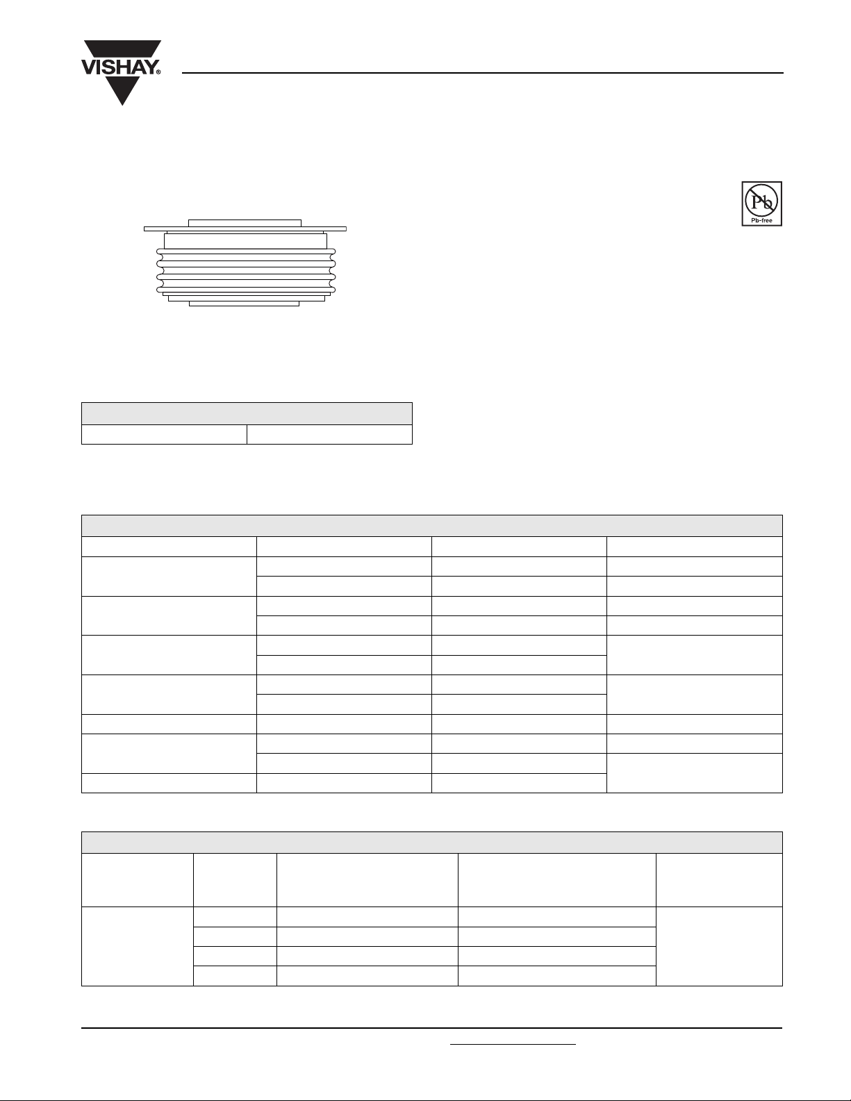
DO-200AB (B-PUK)
PRODUCT SUMMARY
I
F(AV)
SD553C..S50L Series
Vishay High Power Products
Fast Recovery Diodes
(Hockey PUK Version), 560 A
FEATURES
• High power FAST recovery diode series
• 6.0 µs recovery time
• High voltage ratings up to 4500 V
• High current capability
• Optimized turn-on and turn-off characteristics
• Low forward recovery
• Fast and soft reverse recovery
• Press PUK encapsulation
• Case style conform to JEDEC DO-200AB (B-PUK)
• Maximum junction temperature 125 °C
• Lead (Pb)-free
560 A
TYPICAL APPLICATIONS
• Snubber diode for GTO
• High voltage freewheeling diode
• Fast recovery rectifier applications
RoHS
COMPLIANT
MAJOR RATINGS AND CHARACTERISTICS
PARAMETER
I
F(AV)
I
F(RMS)
I
FSM
2
t
I
V
RRM
t
rr
T
J
TEST CONDITIONS VALUES
T
hs
T
hs
50 Hz 12 000
60 Hz 12 570
50 Hz 721
60 Hz 658
Range 3000 to 4500 V
T
J
ELECTRICAL SPECIFICATIONS
VOLTAGE RATINGS
V
, MAXIMUM REPETITIVE
TYPE NUMBER
SD553C..S50L
VOLTAGE
CODE
30 3000 3100
36 3600 3700
40 4000 4100
45 4500 4600
RRM
PEAK REVERSE VOLTAGE
V
560 A
55 °C
1120 A
25 °C
6.0 µs
125
- 40 to 125
V
, MAXIMUM NON-REPETITIVE
RSM
PEAK REVERSE VOLTAGE
V
UNITS
A
kA2s
°C
I
MAXIMUM
RRM
AT T
= 125 °C
J
mA
75
Document Number: 93177 For technical questions, contact: ind-modules@vishay.com
Revision: 14-May-08 1
www.vishay.com
Page 2
SD553C..S50L Series
Vishay High Power Products
Fast Recovery Diodes
(Hockey PUK Version), 560 A
FORWARD CONDUCTION
PARAMETER SYMBOL TEST CONDITIONS VALUES UNITS
Maximum average forward current
at heatsink temperature
Maximum RMS forward current I
Maximum peak, one-cycle forward,
non-repetitive surge current
2
Maximum I
Maximum I
t for fusing I2t
2
√t for fusing I2√t t = 0.1 to 10 ms, no voltage reapplied 7210 kA2√s
Low level value of threshold voltage V
High level value of threshold voltage V
Low level value of forward
slope resistance
High level value of forward
slope resistance
Maximum forward voltage drop V
I
F(AV)
F(RMS)
I
FSM
F(TO)1
F(TO)2
r
f1
r
f2
FM
180° conduction, half sine wave
Double side (single side) cooled
25 °C heatsink temperature double side cooled 1120
t = 10 ms
t = 8.3 ms 12 570
t = 10 ms
t = 8.3 ms 10 570
t = 10 ms
t = 8.3 ms 658
t = 10 ms
t = 8.3 ms 466
(16.7 % x π x I
(I > π x I
(16.7 % x π x I
(I > π x I
No voltage
reapplied
50 % V
RRM
reapplied
No voltage
Sinusoidal half wave,
initial T
= TJ maximum
J
reapplied
50 % V
RRM
reapplied
< I < π x I
F(AV)
), TJ = TJ maximum 1.95
F(AV)
< I < π x I
F(AV)
), TJ = TJ maximum 0.89
F(AV)
), TJ = TJ maximum 1.77
F(AV)
), TJ = TJ maximum 0.98
F(AV)
Ipk = 1500 A, TJ =125 °C, tp = 10 ms sinusoidal wave 3.24 V
560 (210) A
55 (85) °C
12 000
10 100
721
510
A
kA2s
V
mΩ
RECOVERY CHARACTERISTICS
CODE
MAXIMUM VALUE
AT T
= 25 °C
J
t
AT 25 % I
rr
RRM
(µs)
TEST CONDITIONS
I
pk
SQUARE
PULSE
(A/µs)
dI/dt
V
(V)
r
(A)
S50 5.0 1000 100 - 50 6.0 900 250
TYPICAL VALUES
t
AT 25 % I
rr
(µs)
AT TJ = 125 °C
Q
RRM
rr
(µC)
I
(A)
I
FM
rr
t
rr
dir
dt
I
RM(REC)
THERMAL AND MECHANICAL SPECIFICATIONS
PARAMETER SYMBOL TEST CONDITIONS VALUES UNITS
Maximum junction operating
temperature range
Maximum storage temperature range T
Maximum thermal resistance,
junction to heatsink
R
T
J
Stg
thJ-hs
DC operation single side cooled 0.073
DC operation double side cooled 0.031
Mounting force, ± 10 %
Approximate weight 255 g
Case style Conforms to JEDEC DO-200AB (B-PUK)
- 40 to 125
- 40 to 150
14 700
(1500)
°C
K/W
N
(kg)
t
Q
rr
www.vishay.com For technical questions, contact: ind-modules@vishay.com
Document Number: 93177
2 Revision: 14-May-08
Page 3
SD553C..S50L Series
Fast Recovery Diodes
(Hockey PUK Version), 560 A
ΔR
CONDUCTION ANGLE
Note
• The table above shows the increment of thermal resistance R
CONDUCTION
thJ-hs
SINUSOIDAL CONDUCTION RECTANGULAR CONDUCTION
SINGLE SIDE DOUBLE SIDE SINGLE SIDE DOUBLE SIDE
180° 0.009 0.009 0.006 0.006
120° 0.011 0.011 0.011 0.011
90° 0.014 0.014 0.015 0.015
60° 0.020 0.020 0.021 0.021
30° 0.036 0.036 0.036 0.036
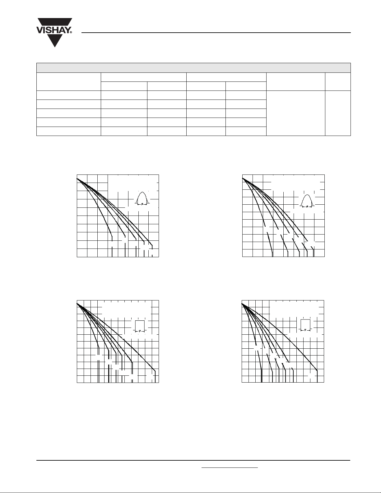
130
120
110
100
90
80
70
60
50
40
30
0100200300400
Maxim um Allowable Heatsink Temperature (°C)
Average Forward Current (A)
SD 553C..S50L Se ries
(Single Side C ooled)
R (DC ) = 0.073 K/W
th J-hs
Cond uction Angl e
60°
30°
90°
120°
180°
Fig. 1 - Current Ratings Characteristics
Vishay High Power Products
TEST CONDITIONS UNITS
T
= TJ maximum K/W
J
when devices operate at different conduction angles than DC
thJ-hs
130
120
110
100
90
80
70
60
50
40
30
20
0 100 200 300 400 500 600 700 800
Maximum Allowable Heatsink Temperature ( °C)
Fig. 3 - Current Ratings Characteristics
SD553C..S50L Series
(D oub le Side Cooled )
R (DC ) = 0.031 K/W
thJ-hs
Conduction Angle
30°
60°
90°
120°
Average Forward C urrent (A)
180°
130
120
110
100
90
80
70
60
50
40
30
20
10
0 1 00 200 300 40 0 5 00 6 00
Maxim um Allowable Heatsink Temperature (°C)
SD 553C ..S50L Series
(Single S ide C ooled)
R ( D C) = 0.073 K/W
thJ-h s
Conduction Period
30°
60°
90°
120°
180° DC
Average Forward Current (A)
Fig. 2 - Current Ratings Characteristics
130
120
110
100
90
80
70
60
50
40
30
20
10
0 200 400 6 00 80 0 100 0 120 0
Maximum Allowable Heatsink Tem perature (°C)
SD553C..S50 L Se ries
(Double S ide Cooled)
R (D C) = 0.031 K/ W
thJ-h s
Conduction Period
30°
60°
90°
120°
180°
Average Forward Curren t (A)
Fig. 4 - Current Ratings Characteristics
DC
Document Number: 93177 For technical questions, contact: ind-modules@vishay.com
www.vishay.com
Revision: 14-May-08 3
Page 4
SD553C..S50L Series
Vishay High Power Products
250 0
225 0
200 0
175 0
150 0
125 0
100 0
750
500
250
Maximum Average Forward Power Loss (W)
3500
3000
2500
2000
1500
1000
500
Maximum Average Forw ard Power Loss (W)
180°
120°
90°
60°
30°
SD553C..S50L Series
T = 125°C
J
0
0 100 200 300 400 500 600 700 800
Averag e Forward C urrent (A)
RMS Limit
Con duction An gle
Fig. 5 - Forward Power Loss Characteristics
DC
180°
120°
90°
60°
30°
RMS Limit
Conduction Period
SD553C ..S50L Series
T = 125°C
J
0
0 200 400 600 800 1000 1200
Ave rage Forward Curre nt (A )
Fig. 6 - Forward Power Loss Characteristics
Fast Recovery Diodes
(Hockey PUK Version), 560 A
14000
12000
10000
8000
6000
4000
Peak Half Sine Wave Forward Current (A)
2000
Fig. 8 - Maximum Non-Repetitive Surge Current
10000
1000
Instan taneous For ward C urrent (A)
100
Fig. 9 - Forward Voltage Drop Characteristics
Maximum Non Repetitive Surge Current
SD553C ..S50L Series
Ve rsus P ulse Train D uration .
50% Rated V Reapplied
Pulse Train Duration (s)
Initial T = 125°C
No Voltage Reapplied
RRM
J
11.010.0
Single and Double Side Cooled
T = 25°C
J
1.522.533.544.55
Instantaneous Forward Voltage (V)
T = 125°C
J
SD553C ..S50L Series
12000
At Any Rated Load Condition And With
50% Ra ted V Ap plied Fo llow ing Surge
11000
10000
9000
8000
7000
6000
5000
SD 553C..S50L Se ries
4000
Pe a k H a lf S in e W a ve F o rw a rd C u rr e n t (A)
3000
Num ber Of E qua l Amp litude Half Cycle C urrent Pulses (N)
RRM
In itia l T = 1 25 °C
J
@ 60 H z 0.0083 s
@ 50 H z 0.0100 s
Fig. 7 - Maximum Non-Repetitive Surge Current
001011
0.1
SD 553 C..S50 L S erie s
thJ-h s
0.01
0.001
Tra nsient Th erm al Im ped an ce Z (K /W )
0. 001 0.0 1 0 .1 1 1 0 10 0
Sq ua re W av e Pu lse Dura tion (s)
Fig. 10 - Thermal Impedance Z
Ste a dy State V alue
R = 0.073 K/W
thJ-hs
(Single S id e C ooled )
R = 0.031 K/W
thJ- hs
(Double Side Cooled)
(D C Op era tio n)
thJ-hs
Characteristic
Single and Double Side Cooled
www.vishay.com For technical questions, contact: ind-modules@vishay.com
Document Number: 93177
4 Revision: 14-May-08
Page 5

SD553C..S50L Series
(Hockey PUK Version), 560 A
400
V
350
300
250
200
150
Forward Recovery (V)
100
50
0
10.5
10
9.5
SD 553 C ..S50L Se ries
T = 1 25 °C; V > 100V
J
9
8.5
8
7.5
I = 15 00 A
FM
Sine Pulse
7
6.5
6
5.5
5
4.5
Maximum Reverse Recovery Time - Trr (µs)
4
10 100 1000
Rate Of Fall Of Forward Current - di/dt (A/µs)
FP
0 200 400 600 800 1000 1200 1400 1600 1800 2000
Fig. 11 - Typical Forward Recovery Characteristics
r
1000 A
500 A
Fast Recovery Diodes
I
SD55 3C..S 50L Series
Rate Of Rise Of Forw ard C urrent - di/dt (A/us)
Vishay High Power Products
T = 12 5°C
J
T = 25°C
J
800
700
600
500
400
300
200
100
0
M ax im um R ev erse Re c ov ery Cu rren t - Ir r (A)
0 5 0 100 1 50 2 00 2 50 300
Rate Of Fall Of Forwa rd Current - di/dt (A/µs)
I = 15 00 A
FM
Sine Pulse
1000 A
500 A
SD 5 5 3C ..S 5 0 L S er ie s
T = 1 2 5 °C ; V > 1 0 0V
J
r
Fig. 12 - Recovery Time Characteristics
2500
2000
1500
1000
500
0
0 50 100 150 200 250 300
Ma x im u m Re ve rse Re co ve ry C h arg e - Q rr (µC )
Rate Of Fall O f Forward Current - di/dt (A/µs)
I = 1 5 00 A
FM
Sin e Pu lse
1000 A
500 A
SD 553C ..S50L Series
T = 1 2 5 °C ; V > 1 0 0V
J r
Fig. 13 - Recovery Charge Characteristics
Fig. 14 - Recovery Current Characteristics
1E4
10 joules per pulse
6
4
2
1
0.8
1E3
Peak Forward Current (A)
1E2
1E1 1E2 1E3 1E4
0.6
0.4
0.2
SD553C..S50L Series
Sinu soid al Pulse
T = 1 25° C, V = 15 00V
J
dv/dt = 1000V/µs
tp
RRM
Pulse B asewidth (µs)
Fig. 15 - Maximum Total Energy Loss
Per Pulse Characteristics
Document Number: 93177 For technical questions, contact: ind-modules@vishay.com
www.vishay.com
Revision: 14-May-08 5
Page 6

SD553C..S50L Series
Vishay High Power Products
1E4
200
400
600
1000
1500
2000
1E3
Peak Forw ard C urrent (A)
1E2
1E1 1E2 1E3 1E4
1E4
1E3
Peak Forward C urrent (A)
1E2
1E1 1E2 1E3 1E4
3000
4000
6000
10000
SD 553 C..S50L Series
Sinu soid al Puls e
T = 55°C , V = 15 00V
C
dv/dt = 1000V/u s
tp
Pulse Basewidth (µs)
Fig. 16 - Frequency Characteristics
SD5 53C.. S5 0L Series
Sin uso ida l Pu lse
T = 125°C, V = 1500V
J
6
4
2
dv/dt = 1000V/µs
10 jo ules p er p ulse
8
tp
1
0.8
0.6
0.4
Pulse Basewidth (µs)
Fig. 17 - Maximum Total Energy Loss
Per Pulse Characteristics
Fast Recovery Diodes
(Hockey PUK Version), 560 A
1E4
100
50 H z
1E3
RRM
Peak Forward Current (A)
1E2
1E4
RRM
1E3
Peak Forward Current (A)
1E2
6000
tp
400 0
3000
2000
1500
100 0
600
400
50 H z
100
200
SD 55 3C.. S50 L Ser ies
Trap ezo idal Pulse
T = 5 5°C, V = 150 0V
dv/dt = 10 00V/us,
di/dt = 300A/us
RRM
C
1E1 1E 2 1E3 1E4
Pulse Basewidth (µs)
Fig. 18 - Frequency Characteristics
SD553C..S50L Series
Tra pezo idal Puls e
T = 125°C, V = 1500V
J
dv/d t = 100 0V/ µs
di/dt = 100A /µs
RRM
0.4
0.6
0.8
tp
10 jo u les p er puls e
8
6
4
2
1
1E1 1E2 1E3 1 E4
Pulse Basewidth (µs)
Fig. 19 - Maximum Total Energy Loss
Per Pulse Characteristics
1E4
tp
400
600
1000
3000
2000
150 0
SD553C..S50L Series
Tra pe zoida l Pu lse
T = 55°C, V = 15 00V
C
dv/dt = 1000V/us,
di/dt = 100A/us
1E3
Peak Forward Current (A)
1E2
4000
6000
1E1 1E2 1E3 1E4
200
100
50 H z
RRM
Pulse Basewidth (µs)
Fig. 20 - Frequency Characteristics
www.vishay.com For technical questions, contact: ind-modules@vishay.com
Document Number: 93177
6 Revision: 14-May-08
Page 7
SD553C..S50L Series
Fast Recovery Diodes
Vishay High Power Products
(Hockey PUK Version), 560 A
ORDERING INFORMATION TABLE
Device code
Dimensions http://www.vishay.com/doc?95246
SD 55 3 C 45 S50 L
51324
1 - Diode
2 - Essential part number
3 - 3 = Fast recovery
4 - C = Ceramic PUK
5 - Voltage code x 100 = V
6 -t
7 - L = PUK case DO-200AB (B-PUK)
code
rr
LINKS TO RELATED DOCUMENTS
67
(see Voltage Ratings table)
RRM
Document Number: 93177 For technical questions, contact: ind-modules@vishay.com
Revision: 14-May-08 7
www.vishay.com
Page 8

Legal Disclaimer Notice
Vishay
Notice
The products described herein were acquired by Vishay Intertechnology, Inc., as part of its acquisition of
International Rectifier’s Power Control Systems (PCS) business, which closed in April 2007. Specifications of the
products displayed herein are pending review by Vishay and are subject to the terms and conditions shown below.
Specifications of the products displayed herein are subject to change without notice. Vishay Intertechnology, Inc., or
anyone on its behalf, assumes no responsibility or liability for any errors or inaccuracies.
Information contained herein is intended to provide a product description only. No license, express or implied, by
estoppel or otherwise, to any intellectual property rights is granted by this document. Except as provided in Vishay's
terms and conditions of sale for such products, Vishay assumes no liability whatsoever, and disclaims any express
or implied warranty, relating to sale and/or use of Vishay products including liability or warranties relating to fitness
for a particular purpose, merchantability, or infringement of any patent, copyright, or other intellectual property right.
The products shown herein are not designed for use in medical, life-saving, or life-sustaining applications.
Customers using or selling these products for use in such applications do so at their own risk and agree to fully
indemnify Vishay for any damages resulting from such improper use or sale.
International Rectifier
are registered trademarks of International Rectifier Corporation in the U.S. and other countries. All other product
names noted herein may be trademarks of their respective owners.
®
, IR®, the IR logo, HEXFET®, HEXSense®, HEXDIP®, DOL®, INTERO®, and POWIRTRAIN
®
Document Number: 99901 www.vishay.com
Revision: 12-Mar-07 1
 Loading...