

DO-200AA
PRODUCT SUMMARY
I
F(AV)
Vishay High Power Products
Standard Recovery Diodes
(Hockey PUK Version), 650 A
FEATURES
• Wide current range
• High voltage ratings up to 3200 V
• High surge current capabilities
• Diffused junction
• Hockey PUK version
• Case style DO-200AA
• Lead (Pb)-free
TYPICAL APPLICATIONS
• Converters
• Power supplies
650 A
• Machine tool controls
• High power drives
• Medium traction applications
SD300C..C Series
RoHS
COMPLIANT
MAJOR RATINGS AND CHARACTERISTICS
PARAMETER TEST CONDITIONS
I
F(AV)
I
F(RMS)
I
FSM
2
t
I
V
RRM
T
J
T
hs
T
hs
50 Hz 6050 6050
60 Hz 6335 6335
50 Hz 183 183
60 Hz 167 167
Range 400 to 2000 2500 to 3200 V
ELECTRICAL SPECIFICATIONS
VOLTAGE RATINGS
V
, MAXIMUM REPETITIVE PEAK
TYPE NUMBER
SD300C..C
VOLTAGE
CODE
04 400 500
08 800 900
12 1200 1300
16 1600 1700
20 2000 2100
25 2500 2600
28 2800 2900
32 3200 3300
RRM
REVERSE VOLTAGE
V
SD300C..C
04 TO 20 25 TO 32
650 540 A
55 55 °C
1150 995 A
25 25 °C
- 40 to 180 - 40 to 150 °C
V
, MAXIMUM NON-REPETITIVE
RSM
PEAK REVERSE VOLTAGE
V
AT T
UNITS
kA2s
I
MAXIMUM
RRM
= TJ MAXIMUM
J
mA
15
A
SD300C..C Series
Vishay High Power Products
Standard Recovery Diodes
(Hockey PUK Version), 650 A
FORWARD CONDUCTION
PARAMETER SYMBOL TEST CONDITIONS
Maximum average forward current
at heatsink temperature
Maximum RMS forward current I
Maximum peak, one-cycle forward,
non-repetitive surge current
Maximum I
Maximum I
2
t for fusing I2t
2
√t for fusing I2√t t = 0.1 to 10 ms, no voltage reapplied 1830 kA2√s
Low level value of threshold voltage V
High level value of threshold voltage V
Low level values of forward
slope resistance
High level values of forward
slope resistance
Maximum forward voltage drop V
I
F(AV)
F(RMS)
I
FSM
F(TO)1
F(TO)2
r
r
180° conduction, half sine wave
Double side (single side) cooled
25 °C heatsink temperature double side cooled 1150 995
t = 10 ms
t = 8.3 ms 6335
t = 10 ms
t = 8.3 ms 5330
t = 10 ms
t = 8.3 ms 167
t = 10 ms
t = 8.3 ms 118
(16.7 % x π x I
(I > π x I
(16.7 % x π x I
f1
(I > π x I
f2
Ipk = 1500 A, TJ = TJ maximum;
FM
t
= 10 ms sinusoidal wave
p
No voltage
reapplied
100 % V
RRM
reapplied
No voltage
Sinusoidal half wave,
initial T
reapplied
100 % V
RRM
reapplied
< I < π x I
F(AV)
), TJ = TJ maximum 1.00
F(AV)
< I < π x I
F(AV)
), TJ = TJ maximum 0.72
F(AV)
F(AV)
F(AV)
SD300C..C
04 TO 20 25 TO 32
650 (380) 540 (250) A
55 (85) 55 (85) °C
6050
5090
= TJ maximum
J
183
129
), TJ = TJ maximum 0.95
), TJ = TJ maximum 0.75
2.08 V
UNITS
A
2
kA
V
mΩ
s
THERMAL AND MECHANICAL SPECIFICATIONS
PARAMETER SYMBOL TEST CONDITIONS
Maximum operating temperature range T
Maximum storage temperature range T
Maximum thermal resistance,
junction to heatsink
R
J
Stg
thJ-hs
DC operation single side cooled 0.163
DC operation double side cooled 0.073
Mounting force, ± 10 % 4900 (500) N (kg)
Approximate weight 70 g
Case style See dimensions - link at the end of datasheet DO-200AA
ΔR
CONDUCTION ANGLE
CONDUCTION
thJ-hs
SINUSOIDAL CONDUCTION RECTANGULAR CONDUCTION
SINGLE SIDE DOUBLE SIDE SINGLE SIDE DOUBLE SIDE
180° 0.017 0.017 0.011 0.012
120° 0.020 0.020 0.020 0.020
90° 0.025 0.025 0.027 0.027
60° 0.036 0.036 0.038 0.038
30° 0.064 0.062 0.065 0.062
Note
• The table above shows the increment of thermal resistance R
when devices operate at different conduction angles than DC
thJ-hs
SD300C..C
04 TO 20 25 TO 32
UNITS
- 40 to 180 - 40 to 150
- 55 to 200
TEST CONDITIONS UNITS
= TJ maximum K/W
T
J
°C
K/W
SD300C..C Series
180
160
140
120
100
80
60
40
Maximum Allowable Heatsink Temperature (°C)
SD30 0C ..C Serie s (400V to 2000V )
0 50 1 0 0 15 0 20 0 25 0 300 35 0 40 0 4 50
Average Forward Current (A)
(Single Side C oo le d)
R (D C ) = 0.163 K /W
th J-hs
Conduction Angle
30°
60°
90°
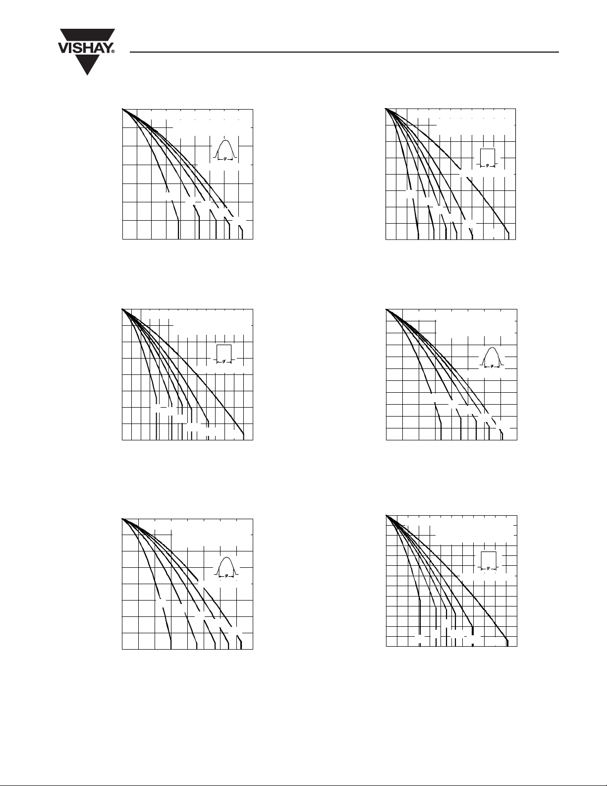
Fig. 1 - Current Ratings Characteristics
180
160
140
120
100
80
60
40
20
Maximum Allowable Heatsink Temperature (°C)
SD30 0C ..C Serie s (400V to 2000V)
30°
0 1 0 0 200 300 400 500 600 700
Average Forward Current (A)
(Single Side Cooled)
R ( D C ) = 0 . 1 63 K /W
thJ-h s
Conduction Period
60°
90°
120°
180°
Fig. 2 - Current Ratings Characteristics
Standard Recovery Diodes
(Hockey PUK Version), 650 A
120°
180°
DC
Vishay High Power Products
180
160
140
120
100
80
60
40
20
Maximum Allowable Heatsink Temperature (°C)
150
140
130
120
110
100
90
80
70
60
50
40
Maximum Allowable Heatsink Temperature (°C)
SD300C..C Series (400V to 2000V)
30°
0 200 400 600 8 00 100 0 1200
Average Forw ard C urrent (A)
(Dou ble Sid e C oo led)
R ( D C ) = 0 .0 7 3 K /W
thJ-h s
Conduction Period
60°
90°
120°
180°
DC
Fig. 4 - Current Ratings Characteristics
SD300C..C Series (2500V to 320 0V)
0 50 100 150 200 250 300 350 400
Average Forward Current (A)
(Single Side Cooled)
R (DC) = 0.163 K/W
thJ- hs
Con duc tion A ngle
30°
60°
90°
120°
180°
Fig. 5 - Current Ratings Characteristics
180
160
140
120
100
80
60
40
20
Maximum Allowable Heatsink Temperature (°C)
SD300C..C Ser ies (400V to 2000V )
0200400600800
Ave rage F orward Current (A)
(Double Side Cooled)
R (DC ) = 0.0 7 3 K /W
thJ-h s
Con duc tion An gle
30°
60°
90°
120°
180°
Fig. 3 - Current Ratings Characteristics
150
140
130
120
110
100
90
80
70
60
50
40
30
20
Maximum Allowable Heatsink Temperature (°C)
SD300C..C Series (2500V to 320 0V )
30°
0 100 200 300 400 500 600
Average Forward Current (A)
(Single Side Cooled)
R (D C ) = 0 .16 3 K / W
th J-hs
Conduction Period
90°
60°
120°
180°
Fig. 6 - Current Ratings Characteristics
DC

SD300C..C Series
Vishay High Power Products
150
140
130
120
110
100
90
80
70
60
50
40
30
20
Maximum Allowable Heatsink Tem perature (°C)
150
140
130
120
110
100
90
80
70
60
50
40
30
20
Maxim um Allowable Heatsink Temperature (°C )
SD300C..C Series (2 500V to 3200V)
0 100 200 300 400 500 600 700
Ave rage F orward Current ( A)
(Double Side Cooled)
R (DC ) = 0 .073 K/W
th J-h s
Conduction Angle
30°
60°
90°
120°
Fig. 7 - Current Ratings Characteristics
SD30 0C ..C Series (2500 V to 3200V)
30°
0 200 400 600 800 1000
Average Forw ard Current (A)
(Dou ble Side C o oled)
R (D C ) = 0.073 K/W
th J-hs
Conduction Period
60°
90°
120°
180°
DC
Fig. 8 - Current Ratings Characteristics
Standard Recovery Diodes
(Hockey PUK Version), 650 A
180°
2500
2000
1500
1000
500
Maxim um Average Forw ard Pow er Loss (W )
DC
180°
120°
90°
60°
30°
RMS Lim it
Conduction Period
SD300C..C Series
T = T m ax .
J
J
0
0 200 400 600 800 1000 1200
Average Forward Current (A)
Fig. 10 - Forward Power Loss Characteristics
6000
At Any Rated Load Condition And W ith
Ra ted V A p p lied Fo llowin g Surg e .
5500
5000
4500
4000
3500
3000
2500
2000
SD300C..C Series
Peak Half Sine W ave Forward Current (A)
1500
Num ber Of Eq ual A mplitud e H alf Cycle Current Pulses (N )
RRM
Init ia l T = T m a x.
JJ
@ 60 H z 0.0083 s
@ 50 H z 0.0100 s
001011
Fig. 11 - Maximum Non-Repetitive Surge Current
Single and Double Side Cooled
180 0
180°
160 0
120°
140 0
120 0
100 0
Maximum Average Forward Power Loss (W)
90°
60°
30°
800
600
400
200
0
0200400600800
Aver a ge Forw ard C urren t (A )
RMS Lim it
Conduction Angle
SD300C..C Series
T = T m ax.
J J
Fig. 9 - Forward Power Loss Characteristics
7000
M a xim u m N o n Rep e titive Su rg e C urre n t
6000
5000
4000
3000
2000
P e a k H a lf S i n e W a v e F o r w a r d C ur r e n t ( A )
SD 300C ..C Se ries
1000
0.01 0.1 1
V e rs u s P u ls e T r a in D u r a tio n .
In it ia l T = T m a x .
N o V o lta g e R e a p p l ie d
Ra ted V Re a p p lie d
RRM
Pulse Train Duration (s)
J
J
Fig. 12 - Maximum Non-Repetitive Surge Current
Single and Double Side Cooled

SD300C..C Series
Standard Recovery Diodes
Vishay High Power Products
(Hockey PUK Version), 650 A
10000
T = 25°C
J
T = T m ax.
J
J
1000
Instant aneous Forw ard Current (A)
100
0.5 1 1.5 2 2.5 3 3.5 4 4.5 5
Instanta ne ous Forwa rd Voltag e (V)
Fig. 13 - Forward Voltage Drop Characteristics
1
Stea d y St ate Va lue
R = 0.163 K/W
thJ-h s
(Single Side C ooled)
th J -hs
R = 0.073 K/W
0.1
thJ-h s
(Dou ble Side Coo led)
(D C O pera tion)
SD300C..C Series
0.01
0.001
Transien t Therm a l Im ped ance Z (K/W )
ORDERING INFORMATION TABLE
Device code
SD 30 0 C 32 C
1 - Diode
2 - Essential part number
3 - 0 = Standard recovery
4 - C = Ceramic PUK
5 - Voltage code x 100 = V
6 - C = PUK case DO-200AA
Sq ua re W a v e Pu lse Du rat ion (s)
Fig. 14 - Thermal Impedance Z
SD 3 0 0C ..C Series
Characteristics
thJC
51324
(see Voltage Ratings table)
RRM
0111.010.0100.0
6

DIMENSIONS in millimeters (inches)
3.5 (0.14) ± 0.1 (0.004) DIA. NOM. x
1.8 (0.07) deep MIN. both ends
Outline Dimensions
Vishay High Power Products
DO-200AA
42 (1.65) DIA. MAX.
19 (0.75) DIA. MAX.
2 places
38 (1.50) DIA. MAX.
Quote between upper and lower pole pieces has to be considered after
application of mounting force (see Thermal and Mechanical Specifications)
0.3 (0.01) MIN.
both ends
14.4 (0.57)
13.7 (0.54)

Legal Disclaimer Notice
Vishay
Disclaimer
All product specifications and data are subject to change without notice.
Vishay Intertechnology, Inc., its affiliates, agents, and employees, and all persons acting on its or their behalf
(collectively, “Vishay”), disclaim any and all liability for any errors, inaccuracies or incompleteness contained herein
or in any other disclosure relating to any product.
Vishay disclaims any and all liability arising out of the use or application of any product described herein or of any
information provided herein to the maximum extent permitted by law. The product specifications do not expand or
otherwise modify Vishay’s terms and conditions of purchase, including but not limited to the warranty expressed
therein, which apply to these products.
No license, express or implied, by estoppel or otherwise, to any intellectual property rights is granted by this
document or by any conduct of Vishay.
The products shown herein are not designed for use in medical, life-saving, or life-sustaining applications unless
otherwise expressly indicated. Customers using or selling Vishay products not expressly indicated for use in such
applications do so entirely at their own risk and agree to fully indemnify Vishay for any damages arising or resulting
from such use or sale. Please contact authorized Vishay personnel to obtain written terms and conditions regarding
products designed for such applications.
Product names and markings noted herein may be trademarks of their respective owners.
 Loading...