

Page 1
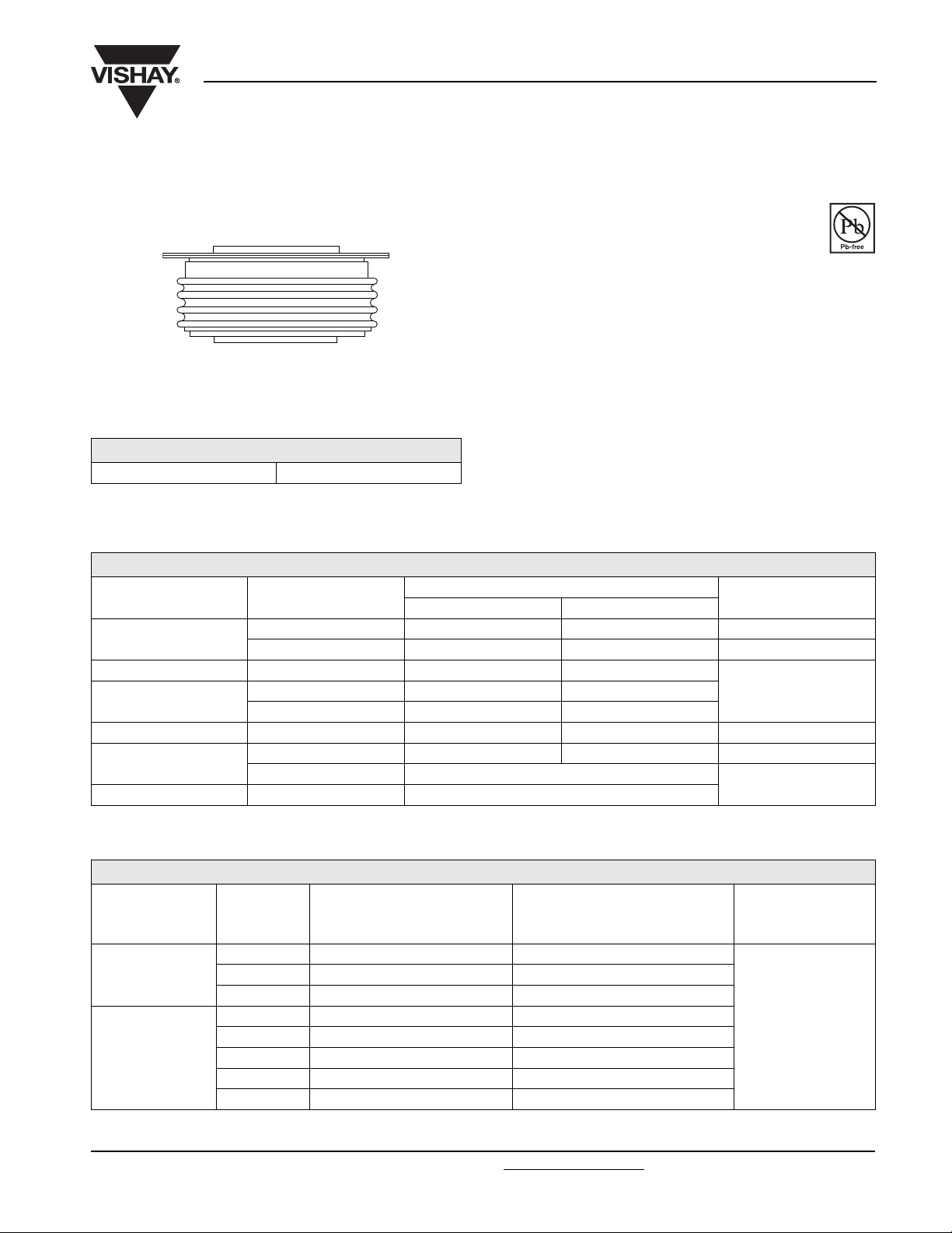
DO-200AC (K-PUK)
PRODUCT SUMMARY
I
F(AV)
SD1553C..K Series
Vishay High Power Products
Fast Recovery Diodes
(Hockey PUK Version), 1650/1825 A
FEATURES
• High power FAST recovery diode series
• 2.0 to 3.0 µs recovery time
• High voltage ratings up to 3000 V
• High current capability
• Optimized turn-on and turn-off characteristics
• Low forward recovery
• Fast and soft reverse recovery
• Press PUK encapsulation
• Case style conform to JEDEC DO-200AC (K-PUK)
• Maximum junction temperature 150 °C
• Lead (Pb)-free
1650/1825 A
TYPICAL APPLICATIONS
• Snubber diode for GTO
• High voltage freewheeling diode
• Fast recovery rectifier applications
RoHS
COMPLIANT
MAJOR RATINGS AND CHARACTERISTICS
PARAMETER TEST CONDITIONS
I
F(AV)
I
F(RMS)
I
FSM
V
RRM
t
rr
T
J
T
hs
50 Hz 25 000 22 000
60 Hz 26 180 23 000
Range 1800 to 2500 1800 to 3000 V
T
J
ELECTRICAL SPECIFICATIONS
VOLTAGE RATINGS
V
, MAXIMUM REPETITIVE
TYPE NUMBER
SD1553C..S20K
SD1553C..S30K
VOLTAGE
CODE
18 1800 1900
22 2200 2300
25 2500 2600
18 1800 1900
22 2200 2300
25 2500 2600
28 2800 2900
30 3000 3100
RRM
PEAK REVERSE VOLTAGE
V
SD1553C..K
S20 S30
1825 1650 A
55 55 °C
3100 2800
2.0 3.0 µs
25
- 40 to 150
V
, MAXIMUM NON-REPETITIVE
RSM
PEAK REVERSE VOLTAGE
V
UNITS
I
MAXIMUM
RRM
= TJ MAXIMUM
AT T
J
A
°C
mA
75
Document Number: 93169 For technical questions, contact: ind-modules@vishay.com
Revision: 14-May-08 1
www.vishay.com
Page 2
SD1553C..K Series
Vishay High Power Products
Fast Recovery Diodes
(Hockey PUK Version),
1650/1825 A
FORWARD CONDUCTION
PARAMETER SYMBOL TEST CONDITIONS
Maximum average forward current
at heatsink temperature
Maximum RMS forward current I
Maximum peak, one-cycle forward,
non-repetitive surge current
2
Maximum I
Maximum I
t for fusing I2t
2
√t for fusing I2√t t = 0.1 to 10 ms, no voltage reapplied 31 260 24 210 kA2√s
Low level value of threshold voltage V
High level value of threshold voltage V
Low level value of forward
slope resistance
High level value of forward
slope resistance
Maximum forward voltage drop V
I
F(AV)
F(RMS)
I
FSM
F(TO)1
F(TO)2
r
r
180° conduction, half sine wave
Double side (single side) cooled
25 °C heatsink temperature double side cooled 3100 2800
t = 10 ms
t = 8.3 ms 26 180 23 000
t = 10 ms
t = 8.3 ms 22 010 19 370
t = 10 ms
t = 8.3 ms 2854 2210
t = 10 ms
t = 8.3 ms 2018 1563
(16.7 % x π x I
(I > π x I
(16.7 % x π x I
f1
(I > π x I
f2
Ipk = 4000 A, TJ = TJ maximum,
FM
= 10 ms sinusoidal wave
t
p
No voltage
reapplied
100 % V
RRM
reapplied
No voltage
Sinusoidal half wave,
initial T
reapplied
100 % V
RRM
reapplied
< I < π x I
F(AV)
), TJ = TJ maximum 1.29 1.45
F(AV)
< I < π x I
F(AV)
), TJ = TJ maximum 0.25 0.30
F(AV)
F(AV)
F(AV)
SD1553C..K
S20 S30
1825 (865) 1650 (790) A
55 (85) 55 (85) °C
25 000 22 000
21 030 18 500
= TJ maximum
J
3126 2421
2210 1712
), TJ = TJ maximum 1.15 1.31
), TJ = TJ maximum 0.27 0.32
2.23 2.60 V
UNITS
A
2
kA
V
mΩ
s
RECOVERY CHARACTERISTICS
CODE
MAXIMUM VALUE
AT T
= 25 °C
J
t
AT 25 % I
rr
RRM
(µs)
TEST CONDITIONS
I
pk
SQUARE
PULSE
(A/µs)
dI/dt
V
(V)
t
r
rr
(A)
S20 2.0
S30 3.0 5.0 780 260
1000 100 - 50
TYPICAL VALUES
AT TJ = 150 °C
AT 25 % I
(µs)
RRM
Q
(µC)
rr
4.5 650 240
I
(A)
I
rr
FM
t
rr
I
RM(REC)
t
Q
rr
dir
dt
THERMAL AND MECHANICAL SPECIFICATIONS
PARAMETER SYMBOL TEST CONDITIONS VALUES UNITS
Maximum junction operating
and storage temperature range
Maximum thermal resistance,
case junction to heatsink
Mounting force, ± 10 %
Approximate weight 425 g
Case style See dimensions - link at the end of datasheet DO-200AC (K-PUK)
www.vishay.com For technical questions, contact: ind-modules@vishay.com
2 Revision: 14-May-08
T
R
, T
J
thJ-hs
Stg
DC operation single side cooled 0.04
DC operation double side cooled 0.02
- 40 to 150 °C
K/W
22 250
(2250)
N
(kg)
Document Number: 93169
Page 3
SD1553C..K Series
Fast Recovery Diodes
(Hockey PUK Version),
1650/1825 A
ΔR
CONDUCTION ANGLE
Note
• The table above shows the increment of thermal resistance R
CONDUCTION
thJ-hs
SINUSOIDAL CONDUCTION RECTANGULAR CONDUCTION
SINGLE SIDE DOUBLE SIDE SINGLE SIDE DOUBLE SIDE
180° 0.0018 0.0019 0.0012 0.0012
120° 0.0021 0.0021 0.0021 0.0021
90° 0.0027 0.0027 0.0029 0.0029
60° 0.0039 0.0039 0.0041 0.0041
30° 0.0067 0.0067 0.0068 0.0068
160
140
120
100
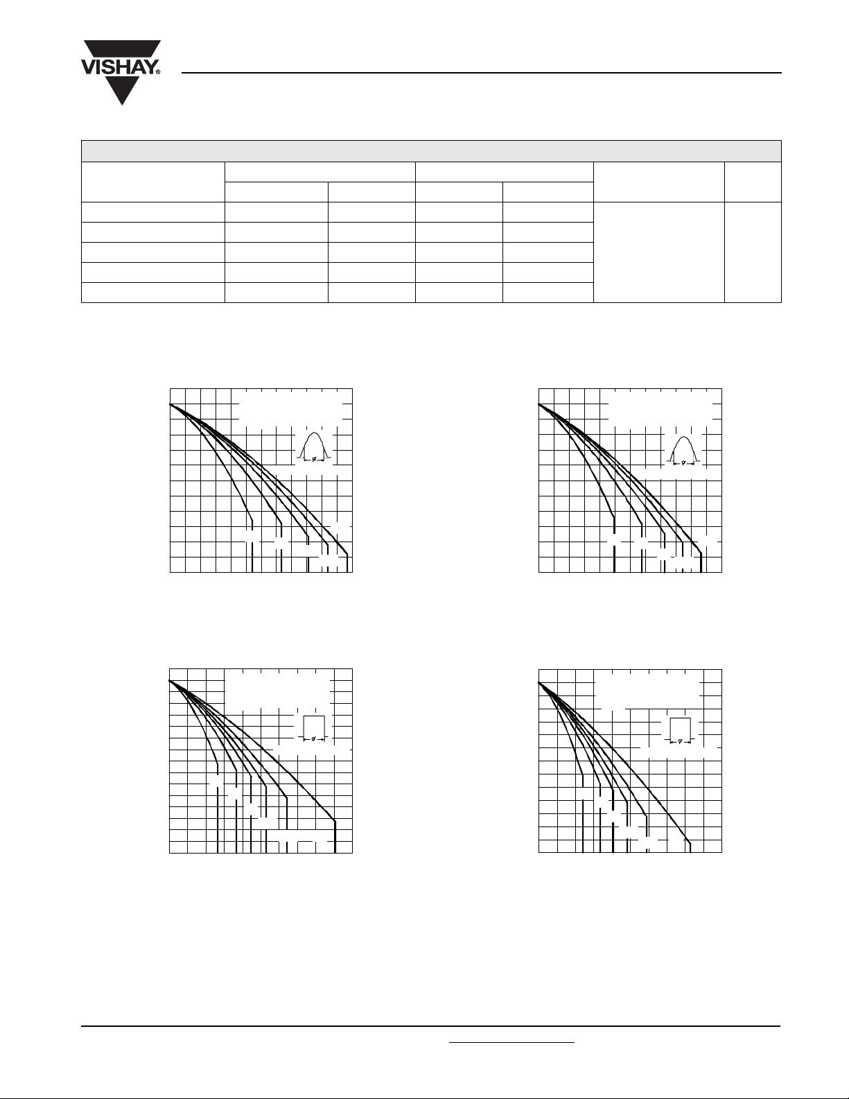
SD 1 553 C ..S20 K S eries
(Single Side Cooled)
R (D C ) = 0.04 K /W
th J-hs
Conduction Angle
Vishay High Power Products
TEST CONDITIONS UNITS
T
= TJ maximum K/W
J
when devices operate at different conduction angles than DC
thJ-hs
160
140
120
100
SD1553C..S30K Series
(Single Side C ooled)
R ( D C) = 0. 04 K/W
thJ-h s
Conduction Angle
80
60
40
0 200 400 600 800 1000 1200
Maxim um Allowable Heatsink Temperature (°C)
A vera g e F orw a rd Curre n t (A)
30°
60°
Fig. 1 - Current Ratings Characteristics
160
140
120
100
80
60
40
20
0
0 400 800 1200 1600 2000
Maximum Allow able Heatsink T emperature (°C)
SD1553C..S20K Series
(Single Side Cooled)
R (DC) = 0.04 K/W
th J-hs
Conduction Period
30°
60°
90°
120°
180° DC
Aver a ge For w ard Curr en t (A )
Fig. 2 - Current Ratings Characteristics
90°
120°
180°
80
60
40
0 200 400 600 80 0 100 0 120 0
Maximum Allowable Heatsink Temperature (°C)
Average Forward Current (A)
30°
60°
90°
Fig. 3 - Current Ratings Characteristics
160
140
120
100
80
60
40
20
0 400 800 1200 1600 2000
Maximum Allowable Heatsink Temperature ( °C)
SD1553C..S30K S eries
(Single Side C ooled)
R (DC) = 0.04 K/W
th J-hs
Conduction Period
30°
60°
90°
120°
180°
Average Forward Current (A)
Fig. 4 - Current Ratings Characteristics
180°
120°
DC
Document Number: 93169 For technical questions, contact: ind-modules@vishay.com
www.vishay.com
Revision: 14-May-08 3
Page 4
SD1553C..K Series
Vishay High Power Products
160
140
120
100
80
60
40
20
0 500 1000 1500 2000 2500
Maxim um A llowable Heatsink Tem perature ( °C)
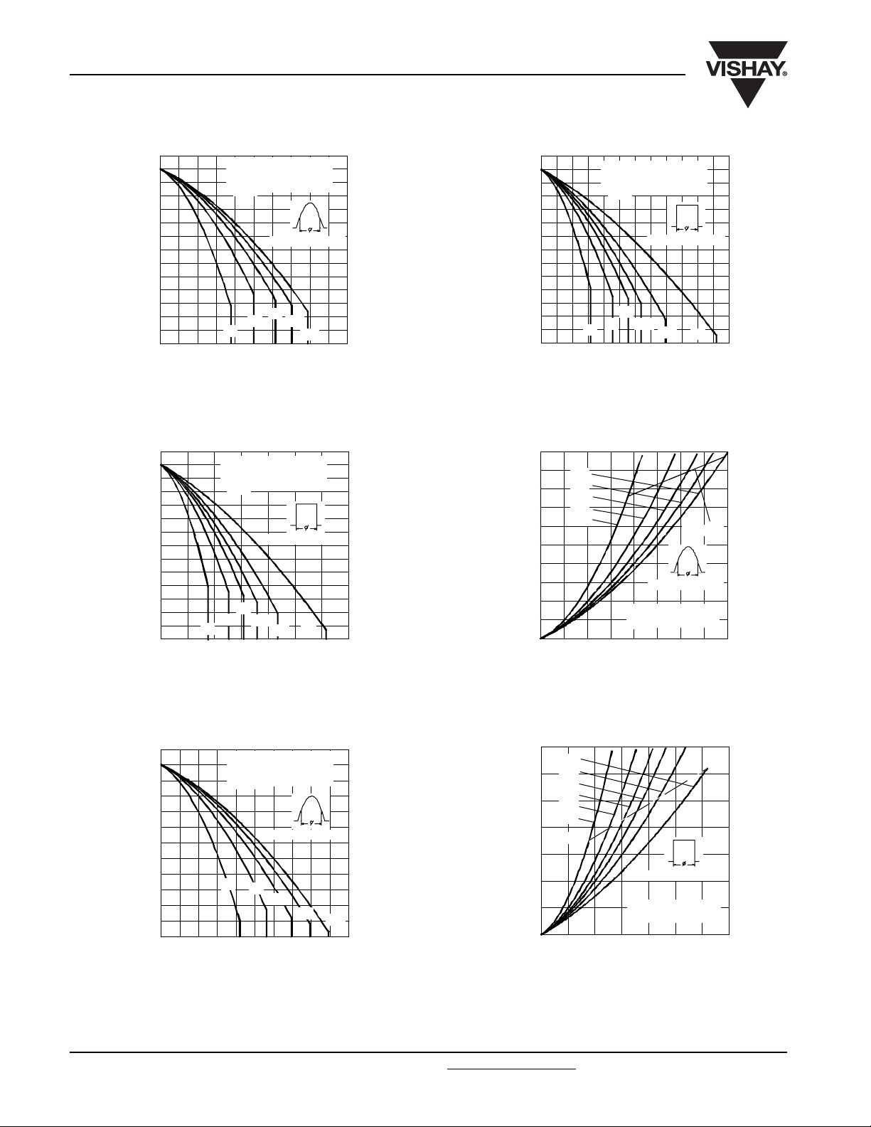
Fig. 5 - Current Ratings Characteristics
160
140
120
100
80
60
40
20
0 500 1000 1500 2000 2500 3000 3500
Maximum Allowable Heatsink Temperature (°C)
Fig. 6 - Current Ratings Characteristics
SD 15 53C ..S20K Serie s
(D o uble S ide C o oled)
R (DC ) = 0.02 K /W
th J-hs
Conduction Angle
90°
60°
30°
Average Forward C urrent (A)
SD1553C..S20K Series
(Double Side Co oled)
R (DC ) = 0. 02 K / W
th J-hs
90°
60°
30°
Average Forward Current (A)
120°
Conduction Period
120°
180°
180°
DC
Fast Recovery Diodes
(Hockey PUK Version),
1650/1825 A
Maximum Allowable H eatsink Temperature (°C)
Maximum A verage Forward Power Loss (W)
160
140
120
100
80
60
40
20
0 500 1000 1500 2000 2500 3000
SD 155 3C ..S3 0K Se r ies
(Double S ide Co oled)
R (DC ) = 0. 02 K / W
th J-hs
Con du ction Pe riod
90°
60°
30°
Average Forward Current (A)
120°
180°
DC
Fig. 8 - Current Ratings Characteristics
5000
4500
4000
3500
3000
2500
2000
1500
1000
500
180°
120°
90°
60°
30°
SD 15 53 C ..S20 K Ser ie s
T = 1 5 0°C
J
0
0 500 1000 1500 2000
Average Forward Current (A)
RMS Limit
Conduction Angle
Fig. 9 - Forward Power Loss Characteristics
160
140
120
100
80
60
40
0 400 800 1200 1600 2000
Maximum Allowable Heatsink Tem perature (°C)
SD1553C..S30K Series
(Double Side Cooled)
R (DC ) = 0.0 2 K/W
th J-hs
Conduction Angle
30°
60°
90°
Averag e Fo rwa rd C urre nt (A)
Fig. 7 - Current Ratings Characteristics
120°
180°
7000
6000
5000
4000
3000
2000
1000
Maximum Average Forward Power Loss (W)
DC
180°
120°
90°
60°
30°
RMS Limit
Conduction Period
SD1553C..S20K Series
T = 150°C
J
0
0 500 1000 1500 2000 2500 3000 3500
Averag e F orwa rd Current (A)
Fig. 10 - Forward Power Loss Characteristics
www.vishay.com For technical questions, contact: ind-modules@vishay.com
Document Number: 93169
4 Revision: 14-May-08
Page 5

SD1553C..K Series
5000
180°
120°
90°
60°
30°
SD1553C..S30K Series
T = 150°C
J
0 500 1000 1500 2000
Average Forward Current (A)
RM S Lim it
Cond uc tion Angle
M aximum Average Forward Power Loss (W)
4000
3000
2000
1000
0
Fig. 11 - Forward Power Loss Characteristics
7000
6000
5000
4000
3000
2000
1000
Maximum Average Forward Power Loss ( W)
DC
180°
120°
90°
60°
30°
RMS Limit
Conduction Period
SD1553C..S30K Series
T = 150°C
J
0
0 500 1000 1500 2000 2500 3000
Ave rage Fo rward Current (A )
Fig. 12 - Forward Power Loss Characteristics
Fast Recovery Diodes
(Hockey PUK Version),
1650/1825 A
Vishay High Power Products
25000
Max imum N on Repetitive Surge Current
22500
20000
17500
15000
12500
10000
7500
SD1553C..S20K Series
Peak Half Sine Wave Forward Current (A)
5000
0.01 0.1 1
Fig. 14 - Maximum Non-Repetitive Surge Current
Single and Double Side Cooled
20000
At An y Ra te d Lo a d C o nd ition A n d W ith
18000
16000
14000
12000
10000
8000
Peak Half Sine W ave Forward Current (A)
6000
Nu mb e r O f Eq ua l A m pl itu d e H a lf C yc le C u rre n t P u l s es (N )
Ra te d V Ap p lie d Fo llow ing Su rg e.
SD15 53C ..S3 0K S eries
Fig. 15 - Maximum Non-Repetitive Surge Current
Single and Double Side Cooled
Versus Pulse Train Duration.
Pulse T rain Duration (s)
RRM
In it ial T = 15 0 ° C
No Voltage Reapplied
Rated V Reapplied
RRM
Initia l T = 150°C
@ 60 Hz 0.0083 s
@ 50 Hz 0.0100 s
J
J
001011
25000
At Any Rated Load Condition And W ith
R a te d V A p p lie d F o llo w in g S u rg e .
22500
20000
17500
15000
12500
10000
SD 1 553 C..S20 K S eries
7500
Peak Half Sine W ave Forward C urrent (A)
5000
Number Of Equal Amplitude Half Cycle Current Pulses (N)
RRM
Init ia l T = 150 °C
J
@ 60 H z 0.0083 s
@ 50 H z 0.0100 s
Fig. 13 - Maximum Non-Repetitive Surge Current
Single and Double Side Cooled
001011
24000
M a xim u m N on Re p etitive S urg e C urre nt
22000
20000
18000
16000
14000
12000
10000
8000
SD 1 553 C ..S 30K S e rie s
6000
Peak Half Sine W ave Forw ard C urren t (A)
4000
0.01 0.1 1
V e rs u s P u ls e Tr a in D u ra t io n .
Pulse Train Duration (s)
Initia l T = 150 °C
N o Vo lta g e R e a p p lie d
Ra ted V Re a p p lie d
RRM
J
Fig. 16 - Maximum Non-Repetitive Surge Current
Single and Double Side Cooled
Document Number: 93169 For technical questions, contact: ind-modules@vishay.com
www.vishay.com
Revision: 14-May-08 5
Page 6

SD1553C..K Series
Vishay High Power Products
10000
T = 25°C
100 0
Instantane ous Forwa rd Current (A )
100
0.511.522.533.54
Instantaneous Forward Voltage (V)
Fig. 17 - Forward Voltage Drop Characteristics Fig. 18 - Forward Voltage Drop Characteristics
J
T = 150°C
J
SD1553C..S20K Series
0.1
Stead y St a te V a lue
R = 0.04 K /W
th J -h s
(Single Side Coo led )
thJ-h s
R = 0.02 K /W
0.01
thJ-hs
(Dou ble Side Co ole d )
(D C O p e ration)
Fast Recovery Diodes
(Hockey PUK Version),
1650/1825 A
Instantaneous Forw ard Current (A)
10000
T = 25°C
J
T = 150°C
J
1000
SD1553C..S30K Series
100
1 1.5 2 2.5 3 3 .5 4 4 .5
Instantaneous Forward V oltage (V)
0.001
SD 1553C ..S20/S30K Series
0.000 1
Transien t Therm al Impedance Z (K/W)
0.001 0.01 0 .1 1 10 100
Squa re W ave Pulse D uration (s)
80
V
F P
60
40
Fo rw a rd R e c ove ry (V )
20
0
0 400 800 1200 1600 2000
Rate Of Rise Of Forw ard Current - di/dt (A/us)
I
T = 150°C
J
T = 25°C
J
SD15 53C ..S20K Serie s
Fig. 19 - Thermal Impedance Z
Characteristic
thJ-hs
Fo rw a rd R ec ov ery (V )
100
V
F P
80
60
40
20
0
0 400 800 120016002000
Ra te Of Rise O f Forwa rd Cu rrent - d i/dt ( A/u s)
I
T = 150°C
J
T = 25°C
J
SD1553C..S30K Series
Fig. 20 - Typical Forward Recovery Characteristics Fig. 21 - Typical Forward Recovery Characteristics
www.vishay.com For technical questions, contact: ind-modules@vishay.com
Document Number: 93169
6 Revision: 14-May-08
Page 7

SD1553C..K Series
Fast Recovery Diodes
(Hockey PUK Version),
7.5
7
6.5
6
5.5
5
4.5
4
3.5
3
Maxim um Reverse Recovery Tim e - Trr (µs)
2.5
Rate Of Fall Of Forward Current - di/dt (A/µs)
Fig. 22 - Recovery Time Characteristics
1400
1200
1000
800
600
400
200
Maximum Reverse Recovery Charge - Qrr (µC)
Rate Of Fall Of Forward Current - di/dt (A/µs)
SD1 553C ..S20K Series
T = 1 50 °C ; V > 100V
rJ
I = 1500 A
FM
Sine Pulse
1000 A
500 A
10 100 1000
I = 15 0 0 A
FM
Sin e Puls e
1000 A
500 A
SD 155 3C..S20K Series
T = 150 °C; V > 100V
J r
0
050100150200250300
1650/1825 A
Vishay High Power Products
8.5
8
7.5
7
6.5
6
5.5
5
4.5
4
Maxim um Reverse Re covery Tim e - Trr (µs)
3.5
Rate Of Fall O f Forward Current - di/dt (A/µs)
Fig. 25 - Recovery Time Characteristics
1600
1400
1200
1000
800
600
400
200
Maximum Reverse Recovery Charge - Qrr (µC)
Rate Of Fall Of Forward Current - di/dt (A/µs)
SD 1553C ..S 30K S eries
T = 150 °C; V > 100V
rJ
I = 150 0 A
FM
Sin e Pulse
1000 A
500 A
10 100 1000
I = 1 50 0 A
FM
Sine Pu lse
1000 A
500 A
SD 1553C ..S3 0K S eries
T = 1 5 0 ° C ; V > 1 0 0V
J r
0
050100150200250300
Fig. 23 - Recovery Charge Characteristics
700
600
I = 1500 A
FM
Sine Pulse
500
400
1000 A
500 A
300
200
SD155 3C ..S20K Serie s
100
0
Maxim um Reverse Recovery Current - Irr (A)
Rate Of Fall Of Forward Current - di/dt (A/µs)
T = 1 50 °C; V > 100V
J
r
0 50 100 150 200 250 300
Fig. 24 - Recovery Current Characteristics
Fig. 26 - Recovery Charge Characteristics
700
600
500
400
300
200
100
0
M axim u m R ev e rse R e c ove ry C urre n t - Irr (A )
0 5 0 10 0 15 0 200 250 300
Ra te Of Fa ll O f Fo rw a rd C u rre n t - di/d t (A/ µs )
I = 1 50 0 A
FM
Sin e Pu lse
1000 A
500 A
SD 15 53 C ..S30K Se ries
T = 150 °C; V > 100V
J
r
Fig. 27 - Recovery Current Characteristics
Document Number: 93169 For technical questions, contact: ind-modules@vishay.com
www.vishay.com
Revision: 14-May-08 7
Page 8

SD1553C..K Series
Vishay High Power Products
1E4
10 jo u le s p e r p ulse
6
4
2
1
0.6
0.4
1E3
Peak Forward Current (A)
1E2
1E1 1E2 1E3 1 E4
Fig. 28 - Maximum Total Energy Loss
1E4
1E3
20000
Peak Forward Current (A)
1E2
1E1 1 E2 1E 3 1 E4
0.2
0.1
SD1 553 C..S20 K Seri es
Sinu soida l Pulse
T = 150°C, V = 800V
tp
dv/dt = 1000V/µs
RRM
J
Pulse Basew idth (µs)
Per Pulse Characteristics
400
400 0
100 0200 0
SD1553C..S20 K Seri es
Sinuso ida l Pulse
T = 55°C , V = 8 00 V
C
dv/dt = 1000V/us
tp
3000
6000
10000
150 00
Pulse Base w idth (µs)
200
RRM
Fast Recovery Diodes
(Hockey PUK Version),
1650/1825 A
50 Hz
100
1E4
100
200
400
600
1000
2000
3000
4000
1E3
Peak Forward Current (A)
1E2
1E1 1 E2 1 E3 1 E4
6000
10000
15000
20000 tp
SD1553C..S20K Series
Tra pe zoid al P u ls e
T = 5 5°C, V = 800V
dv/dt = 1000V/us,
di/dt = 300A/us
RRM
C
Pulse Basewidth (µs)
Fig. 31 - Frequency Characteristics
1E4
10 j o ules p er p ul se
6
4
2
1
1E3
Peak Forward Current (A)
1E2
1E1 1 E2 1E3 1 E4
SD1 553 C ..S20K S eries
Tra pe zoid al P u lse
T = 15 0°C, V = 80 0V
J
dv/dt = 1000V/µs
tp
di/dt = 100A/µs
0.8
0.6
0.4
RRM
Pulse Basewidth (µs)
50 H z
Fig. 29 - Frequency Characteristics
Fig. 32 - Maximum Total Energy Loss
Per Pulse Characteristics
1E4
10 j o ules p er p ul se
6
4
2
1E3
0.4
Peak F orw ard Current (A )
1E2
1E1 1 E2 1 E3 1 E4
SD1 553 C ..S20K S eries
Trap ezoi da l P uls e
T = 150°C, V = 800V
dv/dt = 1000V/µs
tp
di/dt = 300A/µs
1
0.8
0.6
RRM
J
Pulse Basewidth (µs)
Fig. 30 - Maximum Total Energy Loss
1E4
100
200
400
1000
2000
6000
15000
20000
10000
SD1 553C ..S20 K Seri es
Tra p ezo idal Pu lse
T = 55°C , V = 800 V
C
dv/dt = 1000V/us,
tp
di/dt = 100A/us
RRM
1E3
Peak Forward Current (A)
1E2
1E1 1 E2 1 E 3 1 E4
Pulse B ase width (µs)
Fig. 33 - Frequency Characteristics
50 H z
Per Pulse Characteristics
www.vishay.com For technical questions, contact: ind-modules@vishay.com
Document Number: 93169
8 Revision: 14-May-08
Page 9

SD1553C..K Series
1E4
10 joules per pulse
6
4
2
1
0.6
0.4
1E3
Peak Forward Current (A)
1E2
1E1 1E2 1 E3 1 E4
0.2
SD1553C..S30K Series
Sinuso ida l Pul se
T = 150°C, V = 1000V
J
d v/d t = 1 00 0V /µs
tp
RRM
Pulse Basew idth (µs)
Fig. 34 - Maximum Total Energy Loss
Per Pulse Characteristics
1E4
1000
2000
3000
4000
6000
10000
Peak Forward Curren t (A)
1E3
1E1 1 E2 1E3 1 E4
400
SD1553C..S30 K Ser ies
Sin usoid al Pu lse
T = 55°C , V = 1000V
C
dv/dt = 1000V/us
tp
P ulse Base w idt h (µs)
100
RRM
Fast Recovery Diodes
(Hockey PUK Version),
1650/1825 A
1E4
1E3
Peak Forward Current (A)
1E2
1E4
50 Hz200
1E3
Peak Forward Curre nt (A )
1E2
Vishay High Power Products
50 H z
100
200
400
1000
2000
4000
6000
10000
15000
20000
1E1 1E2 1E3 1E4
Pulse Basew idth (µs)
Fig. 37 - Frequency Characteristics
0.8
0.6
SD1 553 C..S30 K Series
Trapezoidal Pulse
T = 150°C, V = 1000V
J
dv/dt = 1000V/µs
tp
di/dt = 100A/µs
1E1 1 E2 1 E3 1 E4
Pulse Basewidth (µs)
SD1553C..S30 K Series
Trapezoidal Pulse
T = 55°C, V = 1000V
C
dv/dt = 1000V/us,
tp
di/dt = 300A/us
6
4
2
1
RRM
RRM
10 joules per pulse
Fig. 35 - Frequency Characteristics
Fig. 38 - Maximum Total Energy Loss
Per Pulse Characteristics
1E4
1 0 j o u les p e r pu ls e
6
4
2
1E3
1
0.8
0.6
Peak Forward Curre nt (A )
1E2
1E1 1E2 1E3 1E4
SD1 553 C ..S30 K Series
Tra pe zoida l Pu lse
T = 150°C, V = 1000V
J
dv/dt = 1000V/µs
tp
d i/dt = 300A /µ s
RRM
Pulse B ase width (µs)
Fig. 36 - Maximum Total Energy Loss
1E4
400
200
600
1000
2000
4000
SD1553C..S30K Series
Peak Forward Current (A)
1E3
1E1 1E2 1E3 1E4
Trap ezoidal Pulse
T = 55°C, V = 1000V
C
dv/dt = 1000V/us,
tp
di/dt = 100A/us
RRM
100
Pulse Basew idth (µs)
Fig. 39 - Frequency Characteristics
50 Hz
Per Pulse Characteristics
Document Number: 93169 For technical questions, contact: ind-modules@vishay.com
www.vishay.com
Revision: 14-May-08 9
Page 10

SD1553C..K Series
Vishay High Power Products
Fast Recovery Diodes
(Hockey PUK Version),
1650/1825 A
ORDERING INFORMATION TABLE
Device code
Dimensions http://www.vishay.com/doc?95247
SD 155 3 C 30 S30 K
51324
67
1
- Diode
2
- Essential part number
3
- 3 = Fast recovery
4
- C = Ceramic PUK
5
- Voltage code x 100 = V
6
-trr code
7
- K = PUK case DO-200AC (K-PUK)
LINKS TO RELATED DOCUMENTS
(see Voltage Ratings table)
RRM
www.vishay.com For technical questions, contact: ind-modules@vishay.com
10 Revision: 14-May-08
Document Number: 93169
Page 11

Legal Disclaimer Notice
Vishay
Notice
The products described herein were acquired by Vishay Intertechnology, Inc., as part of its acquisition of
International Rectifier’s Power Control Systems (PCS) business, which closed in April 2007. Specifications of the
products displayed herein are pending review by Vishay and are subject to the terms and conditions shown below.
Specifications of the products displayed herein are subject to change without notice. Vishay Intertechnology, Inc., or
anyone on its behalf, assumes no responsibility or liability for any errors or inaccuracies.
Information contained herein is intended to provide a product description only. No license, express or implied, by
estoppel or otherwise, to any intellectual property rights is granted by this document. Except as provided in Vishay's
terms and conditions of sale for such products, Vishay assumes no liability whatsoever, and disclaims any express
or implied warranty, relating to sale and/or use of Vishay products including liability or warranties relating to fitness
for a particular purpose, merchantability, or infringement of any patent, copyright, or other intellectual property right.
The products shown herein are not designed for use in medical, life-saving, or life-sustaining applications.
Customers using or selling these products for use in such applications do so at their own risk and agree to fully
indemnify Vishay for any damages resulting from such improper use or sale.
International Rectifier
are registered trademarks of International Rectifier Corporation in the U.S. and other countries. All other product
names noted herein may be trademarks of their respective owners.
®
, IR®, the IR logo, HEXFET®, HEXSense®, HEXDIP®, DOL®, INTERO®, and POWIRTRAIN
®
Document Number: 99901 www.vishay.com
Revision: 12-Mar-07 1
 Loading...