

Vishay High Power Products
Standard Recovery Diodes
(Hockey PUK Version), 1170 A
FEATURES
• Wide current range
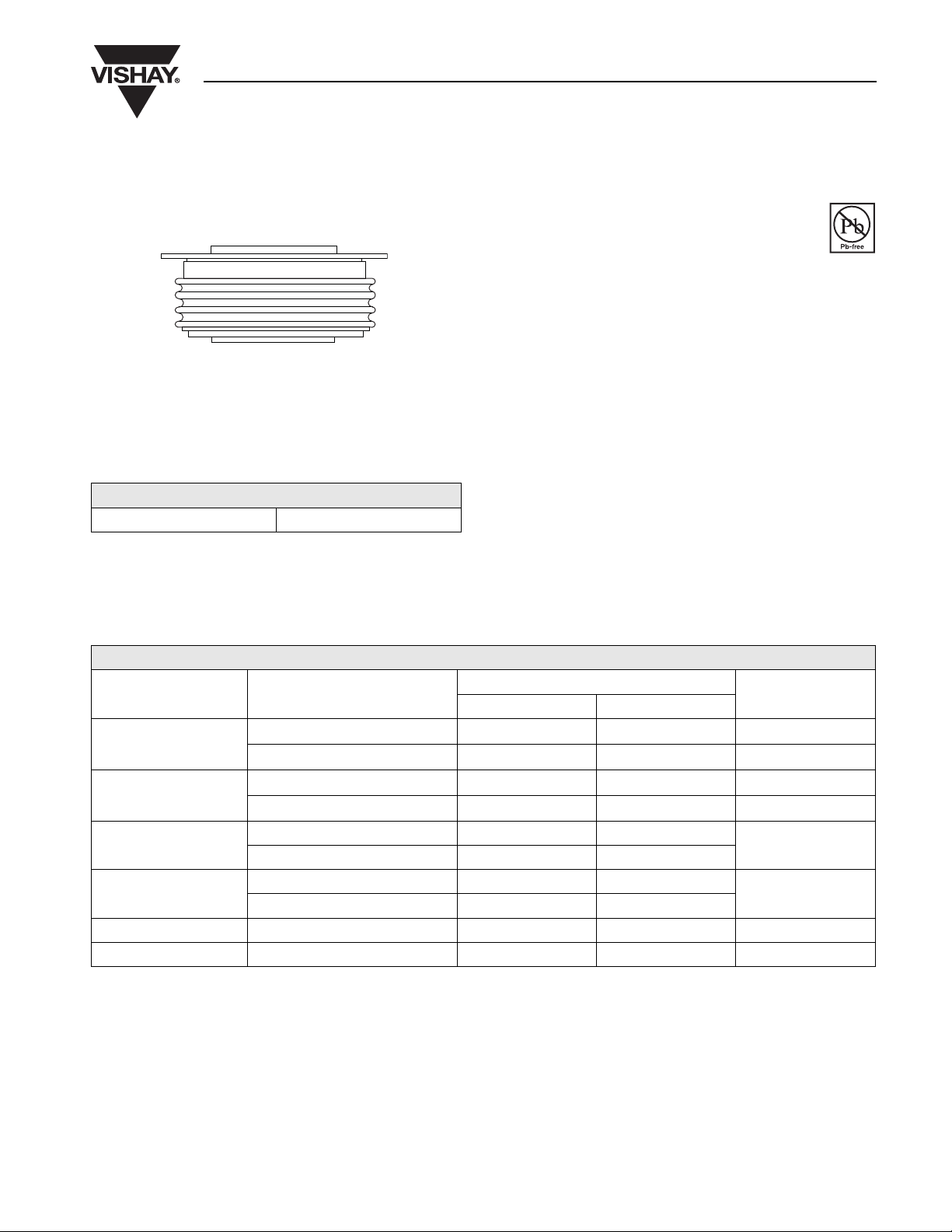
SD1100C..L Series
DO-200AB (B-PUK)
PRODUCT SUMMARY
I
F(AV)
1170 A
MAJOR RATINGS AND CHARACTERISTICS
PARAMETER TEST CONDITIONS
I
F(AV)
I
F(RMS)
I
FSM
2
I
t
V
RRM
T
J
T
hs
T
hs
50 Hz 13 000 10 500
60 Hz 13 600 11 000
50 Hz 846 551
60 Hz 772 503
Range 400 to 2000 2500 to 3200 V
• High voltage ratings up to 3200 V
• High surge current capabilities
• Diffused junction
• Hockey PUK version
• Case style DO-200AB (B-PUK)
• Lead (Pb)-free
• Designed and qualified for industrial level
TYPICAL APPLICATIONS
• Converters
• Power supplies
• Machine tool controls
• High power drives
• Medium traction applications
SD1100C..L
04 to 20 25 to 32
1170 910 A
55 55 °C
2080 1660 A
25 25 °C
- 40 to 180 - 40 to 150 °C
UNITS
kA2s
RoHS
COMPLIANT
A
SD1100C..L Series
Vishay High Power Products
Standard Recovery Diodes
(Hockey PUK Version),
1170 A
ELECTRICAL SPECIFICATIONS
VOLTAGE RATINGS
V
, MAXIMUM REPETITIVE
TYPE NUMBER
VOLTAGE
CODE
RRM
PEAK REVERSE VOLTAGE
V
04 400 500
08 800 900
12 1200 1300
SD1100C..L
16 1600 1700
20 2000 2100
25 2500 2600
30 3000 3100
32 3200 3300
FORWARD CONDUCTION
PARAMETER SYMBOL TEST CONDITIONS
Maximum average forward current
at heatsink temperature
Maximum RMS forward current I
Maximum peak, one-cycle forward,
non-repetitive surge current
Maximum I
Maximum I
2
t for fusing I2t
2
√t for fusing I2√t t = 0.1 to 10 ms, no voltage reapplied 8460 5510 kA2√s
Low level value of threshold voltage V
High level value of threshold voltage V
Low level value of forward
slope resistance
High level value of forward
slope resistance
Maximum forward voltage drop V
I
F(AV)
F(RMS)
I
FSM
F(TO)1
F(TO)2
r
r
180° conduction, half sine wave
Double side (single side) cooled
25 °C heatsink temperature double side cooled 2080 1660
t = 10 ms
t = 8.3 ms 13 600 11 000
t = 10 ms
t = 8.3 ms 11 450 9250
t = 10 ms
t = 8.3 ms 772 503
t = 10 ms
t = 8.3 ms 546 356
(16.7 % x π x I
(I > π x I
(16.7 % x π x I
f1
(I > π x I
f2
Ipk = 1500 A, TJ = TJ maximum,
FM
t
= 10 ms sinusoidal wave
p
No voltage
reapplied
100 % V
reapplied
No voltage
reapplied
100 % V
reapplied
F(AV)
), TJ = TJ maximum 0.94 0.88
F(AV)
F(AV)
), TJ = TJ maximum 0.26 0.38
F(AV)
V
RRM
RRM
< I < π x I
< I < π x I
RSM
PEAK REVERSE VOLTAGE
F(AV)
F(AV)
, MAXIMUM NON-REPETITIVE
AT T
V
SD1100C..L
04 to 20 25 to 32
1170 (600) 910 (420) A
55 (85) 55 (85) °C
13 000 10 500
10 930 8830
Sinusoidal half wave,
initial T
= TJ maximum
J
846 551
598 390
), TJ = TJ maximum 0.78 0.84
), TJ = TJ maximum 0.35 0.40
1.31 1.44 V
I
MAXIMUM
RRM
= TJ MAXIMUM
J
mA
15
UNITS
A
kA2s
V
mΩ
SD1100C..L Series
Standard Recovery Diodes
Vishay High Power Products
(Hockey PUK Version), 1170 A
THERMAL AND MECHANICAL SPECIFICATIONS
PARAMETER SYMBOL TEST CONDITIONS
Maximum junction operating
temperature range
Maximum storage temperature range T
Maximum thermal resistance,
junction to heatsink
Mounting force, ± 10 %
Approximate weight 250 g
Case style See dimensions - link at the end of datasheet DO-200AB (B-PUK)
ΔR
CONDUCTION ANGLE
Note
• The table above shows the increment of thermal resistance R
CONDUCTION
thJ-hs
SINUSOIDAL CONDUCTION RECTANGULAR CONDUCTION
SINGLE SIDE DOUBLE SIDE SINGLE SIDE DOUBLE SIDE
180° 0.011 0.011 0.008 0.008
120° 0.014 0.015 0.014 0.014
90° 0.018 0.018 0.019 0.019
60° 0.026 0.026 0.027 0.028
30° 0.045 0.046 0.046 0.046
R
T
J
Stg
thJ-hs
DC operation single side cooled 0.11
DC operation double side cooled 0.05
when devices operate at different conduction angles than DC
thJ-hs
SD1100C..L
04 to 20 25 to 32
- 40 to 180 - 40 to 150
- 55 to 200
9800
(1000)
TEST CONDITIONS UNITS
= TJ maximum K/W
T
J
UNITS
°C
K/W
N
(kg)

SD1100C..L Series
Vishay High Power Products
180
160
140
120
100
80
60
40
Maximum Allowable Heatsink Temperature (°C)
180
160
140
120
100
80
60
40
20
Maximum Allowable Heatsink Temperature (°C)
SD1100C..L Se ries (400V t o 2000V)
0 200 400 600 800
Average Forward Current (A)
(Single Side Cooled)
R (DC ) = 0.11 K/ W
thJ-hs
Cond uction Angle
30°
60°
90°
120°
Fig. 1 - Current Ratings Characteristics
SD1100C..L Serie s (400V t o 2000V)
30°
0 200 400 600 800 1000 1200
Average Forward Current (A)
(Single Side Cooled)
R (DC ) = 0.11 K/ W
thJ-hs
Cond uction Period
90°
60°
120°
180°
Fig. 2 - Current Ratings Characteristics
Standard Recovery Diodes
(Hockey PUK Version),
1170 A
180°
DC
180
160
140
120
100
80
60
40
20
Maximum Allowa ble Heatsink Temperature (°C)
SD 11 0 0 C . . L Se r i e s ( 4 0 0 V t o 2 00 0 V )
30°
60°
0 500 1000 1500 2000 2500
Average Forward Current (A)
(Double Side Cooled)
R (DC) = 0.05 K/ W
thJ-hs
Conduction Pe riod
90°
120°
180°
Fig. 4 - Current Ratings Characteristics
150
140
130
120
110
100
90
80
70
60
50
40
Maximum Allowable Heatsink Temperature (°C)
SD1100C..L Serie s (2500V t o 3200V)
0 100 200 300 400 500 600 700
Average Forward Current (A)
(Single Side Cooled)
R (DC) = 0.11 K/W
thJ-hs
Conduction Angle
30°
60°
90°
120°
Fig. 5 - Current Ratings Characteristics
DC
180°
180
160
140
120
100
80
60
40
20
Maximum Allowable Heatsink Temperature (°C)
SD1100C..L Series (400V t o 2000V)
0 200 400 600 800 1000 1200 1400
Average Forward Current (A)
(Double Side Cooled)
R (DC) = 0.05 K/W
thJ-hs
Cond uctio n Angle
30°
60°
90°
Fig. 3 - Current Ratings Characteristics
120°
180°
150
140
130
120
110
100
90
80
70
60
50
40
30
20
Maximum Allowab le Heatsink Temperature (°C)
SD1100C..L Se ries (2500V t o 3200V)
30°
0 200 400 600 800 1000
Average Forward Current (A)
(Single Side Cooled)
R (DC) = 0.11 K/ W
thJ-hs
Conduction Period
90°
60°
120°
180°
Fig. 6 - Current Ratings Characteristics
DC

SD1100C..L Series
150
140
130
120
110
100
90
80
70
60
50
40
30
20
Maximum Allowable Heat sink Temperature (°C)
SD1100C. .L Serie s (2500V t o 3200V)
0 200 400 600 800 1000 1200
Average Forward Current (A)
(Double Side Cooled)
R (DC) = 0.05 K/ W
thJ-hs
Cond uction Ang le
30°
60°
90°
120°
Fig. 7 - Current Ratings Characteristics
150
140
130
120
110
100
90
80
70
60
50
40
30
20
Maximum Allowable Heatsink Temperature (°C)
SD1100C..L Serie s (2500V t o 3200V)
30°
60°
0 400 800 1200 1600 2000
Average Forward Current (A)
(Double Side Cooled)
R (DC) = 0.05 K/W
thJ-hs
Cond uction Period
90°
120°
180°
Fig. 8 - Current Ratings Characteristics
Standard Recovery Diodes
(Hockey PUK Version), 1170 A
180°
DC
Vishay High Power Products
3500
DC
180°
3000
120°
90°
2500
60°
30°
2000
1500
1000
500
0
Maximum Average Forward Power Loss (W)
0 500 1000 1500 2000 2500
Average Forward Current (A)
Fig. 10 - Forward Power Loss Characteristics
2000
1800
1600
1400
1200
1000
800
600
400
200
Maximum Average Forward Power Loss (W)
180°
120°
90°
60°
30°
0
0 200 400 600 800 1000 1200
Average Forward Current (A)
Fig. 11 - Forward Power Loss Characteristics
RM S Li m it
Cond uction Period
SD 11 0 0 C . . L Se r i e s
(400V t o 2000V)
T = 180°C
J
RM S Li mi t
Conduction Angle
SD1100C..L Serie s
(2500V to 3200V)
T = 150°C
J
2500
180°
2000
1500
1000
500
Maximum Average Forward Power Loss (W)
120°
90°
60°
30°
0
0 200 400 600 800 1000 1200 1400
Average Forward Current (A)
RM S Li mi t
Cond uc tion Angle
SD1100C..L Serie s
(400V t o 2000V)
T = 18 0° C
J
Fig. 9 - Forward Power Loss Characteristics
2500
DC
180°
2000
120°
90°
60°
30°
1500
1000
500
0
Maximum Average Forward Power Loss (W)
0 400 800 1200 1600 2000
Average Forward Current (A)
RM S Li m it
Cond uction Period
SD 11 00 C . . L Se ri e s
(2500V to 3200V)
T = 150°C
J
Fig. 12 - Forward Power Loss Characteristics

SD1100C..L Series
Vishay High Power Products
12000
At Any Rated Load Condition And With
Rated V Applied Following Surge.
11000
10000
9000
8000
7000
6000
5000
SD1100C..L Serie s
4000
Peak Half Sine Wave Forward Current (A)
(400V to 2000V)
3000
110100
Number Of Equal Amplitude Ha lf Cyc le Current Pulses (N)
Fig. 13 - Maximum Non-Repetitive Surge Current
14000
Maximum Non Repetitive Surge Current
13000
12000
11000
10000
9000
8000
7000
6000
5000
4000
Pe a k Ha l f Sine Wave Forward Current (A)
3000
0.01 0.1 1
Fig. 14 - Maximum Non-Repetitive Surge Current
RRM
Init ial T = 180°C
J
@ 60 Hz 0.0083 s
@ 50 Hz 0.0100 s
Single and Double Side Cooled
Versus Pulse Train Durat ion.
SD1100C..L Serie s
(400V to 2000V)
Pulse Tra in D u r a tio n ( s)
Init ial T = 180 °C
No Voltage Reapplied
Ra t e d V Re a p p l i e d
J
RRM
Single and Double Side Cooled
Standard Recovery Diodes
(Hockey PUK Version),
1170 A
11000
10000
9000
8000
7000
6000
5000
4000
Peak Half Sine Wave Forward Current (A)
3000
Fig. 16 - Maximum Non-Repetitive Surge Current
10000
1000
Instantaneous Forward Current (A)
Fig. 17 - Forward Voltage Drop Characteristics
Maximum Non Repetitive Surge Current
SD1100C..L Se ries
(2500V to 3200V)
0.01 0.1 1
Versus Pulse Train Durat ion.
Pul se Tra in Du ra tio n ( s)
Init ial T = 150 ° C
No Voltage Reapplied
Ra t e d V Re a p p l ie d
RRM
J
Single and Double Side Cooled
T = 2 5° C
J
T = 18 0° C
J
SD 11 0 0 C .. L Se r ie s
(400V to 2000V)
100
0.511.522.53 3.54
Instantaneous Forward Voltage (V)
10000
At Any Rated Load Condition And With
Rated V Applied Following Surge.
9000
8000
7000
6000
5000
SD1100C. .L Serie s
4000
Peak Half Sine Wave Forward Current (A)
(2500V to 3200V)
3000
110100
Numb er Of Equa l Amplit ude Half Cyc le Current Pulses (N)
RRM
Init ial T = 150° C
J
@ 60 Hz 0.0083 s
@ 50 Hz 0.0100 s
Fig. 15 - Maximum Non-Repetitive Surge Current
Single and Double Side Cooled
10000
T = 25 °C
J
T = 1 5 0° C
J
1000
SD1100C..L Series
Instantaneous Forward Current (A)
100
0.5 1 1.5 2 2.5 3 3.5 4 4.5 5
Instantaneous Forward Voltage (V)
(2500V t o 3200V)
Fig. 18 - Forward Voltage Drop Characteristics

SD1100C..L Series
Standard Recovery Diodes
(Hockey PUK Version), 1170 A
1
Steady State Value
R = 0.11 K/ W
thJ-hs
thJ-hs
Transient Therma l Imp ed anc e Z (K/W)
ORDERING INFORMATION TABLE
Device code
(Single Side Cooled)
R = 0.05 K/ W
0.1
thJ-hs
(Double Side Cooled)
(DC Operation)
0.01
0.001
0.00 1 0.01 0.1 1 10
Fig. 19 - Thermal Impedance Z
SD 110 0 C 32 L
SD 1 10 0 C . . L Se r i e s
Sq uare Wave Pulse Duration (s)
Characteristics
thJC
Vishay High Power Products
1
- Diode
2
- Essential part number
3
- 0 = Standard recovery
4
- C = Ceramic PUK
5
- Voltage code x 100 = V
6
- L = PUK case DO-200AB (B-PUK)
51324
6
(see Voltage Ratings table)
RRM

Outline Table
3.5(0.14) DIA. NOM. x
1.8(0.07) DEEP MIN.
58.5 (2 .3 0) DIA . M AX .
0.8 (0.03)
BOTH ENDS
SD1100C..L Series
BOTH ENDS
Case Style DO-200AB (B-PUK)
All dimensions in millimeters (inches)
34 (1.34) DIA. MAX.
TWO PLACES
25 .4 (1 )
26.9 (1.06)
53 (2.09) DIA. MAX.
F

Legal Disclaimer Notice
Vishay
Notice
The products described herein were acquired by Vishay Intertechnology, Inc., as part of its acquisition of
International Rectifier’s Power Control Systems (PCS) business, which closed in April 2007. Specifications of the
products displayed herein are pending review by Vishay and are subject to the terms and conditions shown below.
Specifications of the products displayed herein are subject to change without notice. Vishay Intertechnology, Inc., or
anyone on its behalf, assumes no responsibility or liability for any errors or inaccuracies.
Information contained herein is intended to provide a product description only. No license, express or implied, by
estoppel or otherwise, to any intellectual property rights is granted by this document. Except as provided in Vishay's
terms and conditions of sale for such products, Vishay assumes no liability whatsoever, and disclaims any express
or implied warranty, relating to sale and/or use of Vishay products including liability or warranties relating to fitness
for a particular purpose, merchantability, or infringement of any patent, copyright, or other intellectual property right.
The products shown herein are not designed for use in medical, life-saving, or life-sustaining applications.
Customers using or selling these products for use in such applications do so at their own risk and agree to fully
indemnify Vishay for any damages resulting from such improper use or sale.
®
International Rectifier
are registered trademarks of International Rectifier Corporation in the U.S. and other countries. All other product
names noted herein may be trademarks of their respective owners.
, IR®, the IR logo, HEXFET®, HEXSense®, HEXDIP®, DOL®, INTERO®, and POWIRTRAIN
®
 Loading...