

DO-200AB (B-PUK)
PRODUCT SUMMARY
I
F(AV)
SD1053C..L Series
Vishay High Power Products
Fast Recovery Diodes
(Hockey PUK Version), 920/1050 A
FEATURES
• High power FAST recovery diode series
• 2.0 to 3.0 µs recovery time
• High voltage ratings up to 3000 V
• High current capability
• Optimized turn-on and turn-off characteristics
• Low forward recovery
• Fast and soft reverse recovery
• Press PUK encapsulation
• Case style conform to JEDEC DO-200AB (B-PUK)
• Maximum junction temperature 150 °C
• RoHS compliant
• Lead (Pb)-free
• Designed and qualified for industrial level
920/1050 A
TYPICAL APPLICATIONS
• Snubber diode for GTO
• High voltage freewheeling diode
• Fast recovery rectifier applications
RoHS
COMPLIANT
MAJOR RATINGS AND CHARACTERISTICS
PARAMETER TEST CONDITIONS
I
F(AV)
I
F(RMS)
I
FSM
V
RRM
t
rr
T
J
T
hs
50 Hz 15 000 13 000
60 Hz 15 700 13 610
Range 1800 to 2500 1800 to 3000 V
T
J
ELECTRICAL SPECIFICATIONS
VOLTAGE RATINGS
V
, MAXIMUM REPETITIVE
TYPE NUMBER
SD1053C..S20L
SD1053C..S30L
VOLTAGE
CODE
18 1800 1900
22 2200 2300
25 2500 2600
18 1800 1900
22 2200 2300
25 2500 2600
28 2800 2900
30 3000 3100
RRM
PEAK REVERSE VOLTAGE
V
SD1053C..L
S20 S30
1050 920 A
55 55 °C
1940 1700
2.0 3.0 µs
25
- 40 to 150
V
, MAXIMUM NON-REPETITIVE
RSM
PEAK REVERSE VOLTAGE
V
UNITS
I
MAXIMUM
RRM
AT T
= TJ MAXIMUM
J
A
°C
mA
50
Document Number: 93167 For technical questions, contact: ind-modules@vishay.com
Revision: 14-May-08 1
www.vishay.com
SD1053C..L Series
Vishay High Power Products
Fast Recovery Diodes
(Hockey PUK Version),
920/1050 A
FORWARD CONDUCTION
PARAMETER SYMBOL TEST CONDITIONS
Maximum average forward current
at heatsink temperature
Maximum RMS forward current I
Maximum peak, one-cycle forward,
non-repetitive surge current
Maximum I
Maximum I
2
t for fusing I2t
2
√t for fusing I2√t t = 0.1 to 10 ms, no voltage reapplied 11 250 8450 kA2√s
Low level value of threshold voltage V
High level value of threshold voltage V
Low level value of forward
slope resistance
High level value of forward
slope resistance
Maximum forward voltage drop V
I
F(AV)
F(RMS)
I
FSM
F(TO)1
F(TO)2
r
r
180° conduction, half sine wave
Double side (single side) cooled
25 °C heatsink temperature double side cooled 1940 1700
t = 10 ms
t = 8.3 ms 15 700 13 610
t = 10 ms
t = 8.3 ms 13 210 11 450
t = 10 ms
t = 8.3 ms 1027 772
t = 10 ms
t = 8.3 ms 727 546
(16.7 % x π x I
(I > π x I
(16.7 % x π x I
f1
(I > π x I
f2
Ipk = 1500 A, TJ = TJ maximum,
FM
t
= 10 ms sinusoidal wave
p
No voltage
reapplied
100 % V
reapplied
No voltage
RRM
Sinusoidal half wave,
initial T
reapplied
100 % V
RRM
reapplied
< I < π x I
F(AV)
), TJ = TJ maximum 1.48 1.67
F(AV)
< I < π x I
F(AV)
), TJ = TJ maximum 0.33 0.45
F(AV)
F(AV)
F(AV)
SD1053C..L
S20 S30
1050 (450) 920 (390) A
55 (85) 55 (85) °C
15 000 13 000
12 620 10 930
= TJ maximum
J
1125 845
796 598
), TJ = TJ maximum 1.34 1.51
), TJ = TJ maximum 0.37 0.50
1.90 2.26 V
UNITS
A
2
kA
V
mΩ
s
RECOVERY CHARACTERISTICS
TYPICAL VALUES
AT TJ = 150 °C
AT 25 % I
(µs)
RRM
Q
(µC)
rr
4.0 400 180
I
(A)
I
rr
FM
t
rr
I
RM(REC)
t
Q
rr
dir
dt
CODE
MAXIMUM VALUE
= 25 °C
AT T
J
AT 25 % I
t
rr
RRM
(µs)
TEST CONDITIONS
I
pk
SQUARE
PULSE
(A/µs)
dI/dt
V
(V)
t
r
rr
(A)
S20 2.0
S30 3.0 4.5 550 230
1000 100 - 50
THERMAL AND MECHANICAL SPECIFICATIONS
PARAMETER SYMBOL TEST CONDITIONS VALUES UNITS
Maximum junction operating
and storage temperature range
Maximum thermal resistance,
case junction to heatsink
Mounting force, ± 10 %
Approximate weight 255 g
Case style See dimensions - link at the end of datasheet DO-200AB (B-PUK)
www.vishay.com For technical questions, contact: ind-modules@vishay.com
2 Revision: 14-May-08
T
J
R
, T
thJ-hs
Stg
DC operation single side cooled 0.073
DC operation double side cooled 0.031
- 40 to 150 °C
K/W
14 700
(1500)
(kg)
N
Document Number: 93167
SD1053C..L Series
Fast Recovery Diodes
(Hockey PUK Version),
920/1050 A
ΔR
CONDUCTION ANGLE
Note
• The table above shows the increment of thermal resistance R
CONDUCTION
thJ-hs
SINUSOIDAL CONDUCTION RECTANGULAR CONDUCTION
SINGLE SIDE DOUBLE SIDE SINGLE SIDE DOUBLE SIDE
180° 0.009 0.008 0.006 0.006
120° 0.011 0.011 0.011 0.011
90° 0.014 0.014 0.015 0.015
60° 0.020 0.021 0.021 0.022
30° 0.036 0.036 0.036 0.036
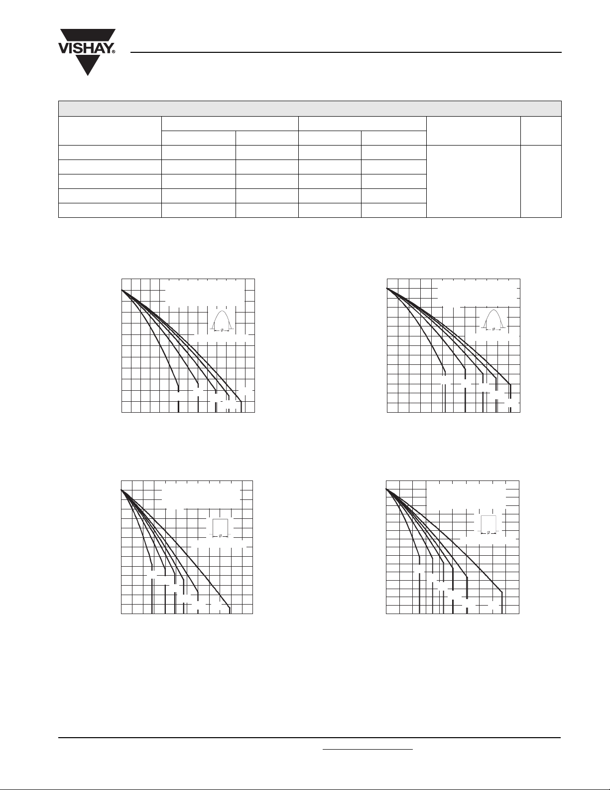
160
140
120
100
80
60
40
0 100 200 300 400 500 600 700
Maximum Allowable Heatsink Temperature (°C)
SD1053C .. S20L Se ries
(Single Side Cooled)
R ( DC) = 0.073 K/W
thJ-hs
Cond uc tion Angle
60°
30°
Average Forward Current (A)
90°
120°
180°
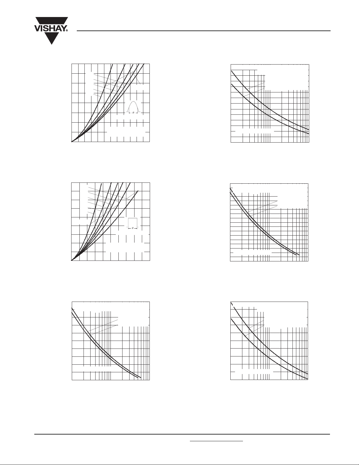
Fig. 1 - Current Ratings Characteristics
Vishay High Power Products
TEST CONDITIONS UNITS
= TJ maximum K/W
T
J
when devices operate at different conduction angles than DC
thJ-hs
160
140
120
100
80
60
40
20
0 100 200 300 400 500 600
Maximum Allowable Heatsink Temperature (°C)
Average Forward Current (A)
Fig. 3 - Current Ratings Characteristics
SD1053C ..S30L Serie s
(Single Side Cooled)
R ( DC) = 0.073 K/W
thJ-hs
Cond uctio n Angle
30°
60°
90°
120°
180°
160
140
120
100
80
60
40
20
0 200 400 600 800 1000 1200
Maximum Allowable Heatsink Temperature (°C)
SD 1 0 5 3C . . S20L Serie s
(Single Side Cooled)
R (DC) = 0.073 K/ W
thJ-hs
Conduction Period
30°
60°
90°
120°
180°
DC
Average Forward Current (A)
Fig. 2 - Current Ratings Characteristics
160
140
120
100
80
60
40
20
0
0 200 400 600 800 1000
Maximum Allowable Heatsink Temperature (°C)
SD 1 05 3 C . .S3 0L Se r i e s
(Sing le Side Cooled)
R (DC) = 0.073 K/ W
thJ-hs
Conduction Period
30°
60°
90°
120°
180°
Average Forward Current (A)
Fig. 4 - Current Ratings Characteristics
DC
Document Number: 93167 For technical questions, contact: ind-modules@vishay.com
www.vishay.com
Revision: 14-May-08 3
SD1053C..L Series
Vishay High Power Products
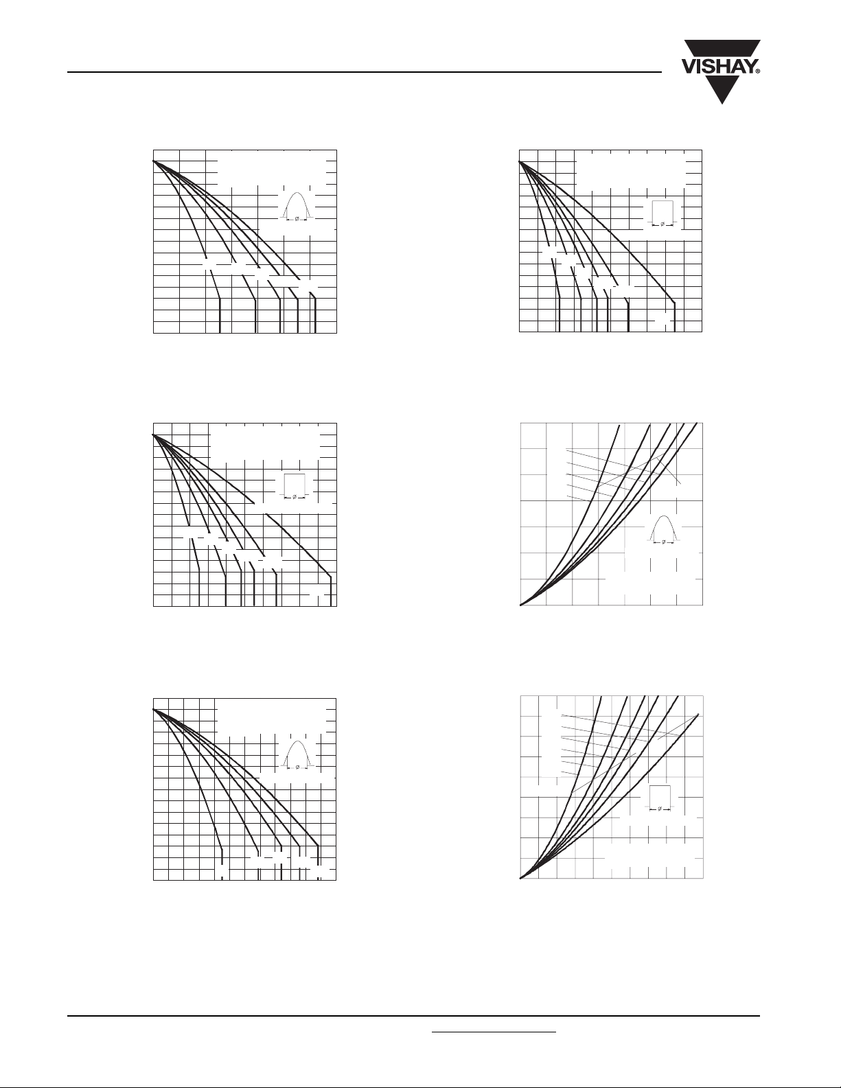
160
140
120
100
80
60
40
20
0
0 200 400 600 800 1000 1200 1400
Maximum Allowable Heatsink Te mperature (°C)
Fig. 5 - Current Ratings Characteristics
160
140
120
100
80
60
40
20
0
0 400 800 1200 1600 2000
Maximum Allowable Heatsink Temperature (°C)
Fig. 6 - Current Ratings Characteristics
SD1053C..S20L Serie s
(Double Side Cooled)
R (DC) = 0.031 K/W
thJ-hs
Conduction Angle
30°
60°
90°
120°
180°
Average Forward Current (A)
SD1053C ..S20L Se ries
(Double Side Cooled)
R (DC) = 0.031 K/W
thJ-hs
Conduction Period
30°
60°
90°
120°
180°
Average Forward Current (A)
Fast Recovery Diodes
(Hockey PUK Version),
920/1050 A
DC
160
140
120
100
80
60
40
20
0
0 400 800 120016002000
Maximum Allowa ble Heatsink Temp erature (°C)
SD 10 5 3 C .. S3 0L Se r i e s
(Double Side Cooled)
R (DC) = 0.031 K/ W
thJ-hs
Cond uction Period
30°
60°
90°
120°
180°
DC
Average Fo rward Current (A)
Fig. 8 - Current Ratings Characteristics
3500
3000
2500
2000
1500
1000
500
Maximum Average Forward Power Loss (W)
180°
120°
90°
60°
30°
SD 1 0 53 C . . S2 0L Se r i e s
T = 150°C
J
0
0 200 400 600 800 1000 1200 1400
Ave ra g e Forwa rd Current (A)
RM S Li m it
Cond uction Angle
Fig. 9 - Forward Power Loss Characteristics
160
140
120
100
80
60
40
20
0
0 200 400 600 800 1000 1200
Maximum Allowable Heatsink Temperature (°C)
SD1053C..S30L Seri es
(Double Side Cooled)
R (DC) = 0.031 K/ W
thJ-hs
Conduction Angle
90°
60°
30°
Average Forward Current (A)
Fig. 7 - Current Ratings Characteristics
120°
180°
4500
4000
3500
3000
2500
2000
1500
1000
500
Maximum Average Forward Power Loss (W)
DC
180°
120°
90°
60°
30°
RM S L i m i t
Conduction Period
SD1053C ..S20L Se rie s
T = 150°C
J
0
0 400 800 120016002000
Av era ge Fo rwa rd Curren t ( A)
Fig. 10 - Forward Power Loss Characteristics
www.vishay.com For technical questions, contact: ind-modules@vishay.com
Document Number: 93167
4 Revision: 14-May-08
SD1053C..L Series
3200
Maximum Average Forwa rd Power Loss (W)
2800
2400
2000
1600
1200
800
400
0
180°
120°
90°
60°
30°
SD1053C..S30L Se rie s
T = 150°C
J
0 200 400 600 800 1000 1200
Average Forward Current (A)
RM S Li m i t
Conduction Angle
Fig. 11 - Forward Power Loss Characteristics
4500
4000
3500
3000
2500
2000
1500
1000
500
Maximum Average Forward Power Loss (W)
DC
180°
120°
90°
60°
30°
RM S Li m i t
Conduction Period
SD1053C ..S30L Serie s
T = 1 50 °C
J
0
0 400 800 120016002000
Average Forward Current (A)
Fig. 12 - Forward Power Loss Characteristics
Fast Recovery Diodes
(Hockey PUK Version),
920/1050 A
Vishay High Power Products
16000
Maximum Non Rep etitive Surge Current
14000
12000
10000
8000
6000
SD1053C ..S20L Se ries
4000
Peak Half Sine Wave Forward Current (A)
2000
0.01 0.1 1
Fig. 14 - Maximum Non-Repetitive Surge Current
12000
At Any Rat ed Lo ad Cond itio n And With
11000
10000
9000
8000
7000
6000
5000
4000
Pe ak Ha l f Sine Wav e Fo rward Curre nt (A)
3000
Number Of Eq ual Amp litude Half Cyc le Current Pulses (N)
Rated V A p plied Following Surg e.
SD1053C ..S30L Se ries
110100
Fig. 15 - Maximum Non-Repetitive Surge Current
Single and Double Side Cooled
Ve rsus Pulse Trai n Dura tio n.
Pulse Train Duration (s)
RRM
Initia l T = 150 °C
No Voltage Reapplied
Rated V Rea pplied
RRM
Init ial T = 150°C
@ 60 Hz 0.0083 s
@ 50 Hz 0.0100 s
J
J
14000
At Any Ra ted Load Co ndition And With
13000
12000
11000
10000
Peak Half Sine Wave Forward Current (A)
Numbe r Of Eq ual Am plitud e Half Cyc le Current Pulses (N)
Rated V App lied Following Surg e.
RRM
9000
8000
7000
6000
SD1053C ..S20L Se rie s
5000
4000
110100
Init ial T = 150 °C
J
@ 60 Hz 0.0083 s
@ 50 Hz 0.0100 s
Fig. 13 - Maximum Non-Repetitive Surge Current
13000
Maximum Non Repet itive Surge Current
12000
11000
10000
9000
8000
7000
6000
5000
SD1053C. .S30L Series
4000
Pe ak Ha lf Sine Wave Forward Current (A)
3000
0.01 0.1 1
Versus Pulse Train Durat ion.
Pul se Tr a in Dura t io n ( s)
Init ial T = 150 °C
No Voltage Reapplied
Rated V Reapplied
RRM
J
Fig. 16 - Maximum Non-Repetitive Surge Current
Single and Double Side Cooled
Document Number: 93167 For technical questions, contact: ind-modules@vishay.com
www.vishay.com
Revision: 14-May-08 5

SD1053C..L Series
Vishay High Power Products
10000
T = 2 5° C
J
T = 1 50 °C
J
1000
SD1053C ..S20L Se ries
Instantaneous Forward Current (A)
100
11.522.533.544.55
Instant aneous Forward Voltage (V)
Fig. 17 - Forward Voltage Drop Characteristics Fig. 18 - Forward Voltage Drop Characteristics
0.1
SD1053C..S20/ S30L Series
thJ-hs
Fast Recovery Diodes
(Hockey PUK Version),
920/1050 A
10000
Instantaneous Forward Current (A)
T = 25 ° C
J
T = 1 50 °C
J
1000
SD 10 5 3 C .. S3 0L Se r ie s
100
1 1.5 2 2.5 3 3.5 4 4.5 5 5.5 6 6.5
Instantaneous Forward Voltage (V)
0.01
0.00 1
Transient Thermal Impedance Z (K/W)
0.001 0.01 0.1 1 10 100
100
V
FP
80
60
40
Fo rw a r d Re c o v ery (V )
20
0
0 400 800 1200 1600 2000
Ra t e O f Ri se O f Fo rw a r d C u rr e n t - d i/ d t ( A/ u s)
I
T = 1 5 0° C
J
T = 25 ° C
J
SD1053C ..S20L Se rie s
Sq ua re Wa ve Pulse D ura tio n (s)
Fig. 19 - Thermal Impedance Z
St e a d y St a t e V a l u e
R = 0.073 K/ W
thJ-hs
(Single Side Cooled)
R = 0.031 K/ W
thJ-hs
(Double Side Co oled )
(DC Op eration)
Characteristic
thJ-hs
160
120
80
Forward Recovery (V)
40
0
0 400 800 1200 1600 2000
Rate Of Rise Of Forward Current - di/dt (A/us)
V
FP
T = 150°C
J
I
T = 2 5 ° C
J
SD1053C..S30L Series
Fig. 20 - Typical Forward Recovery Characteristics Fig. 21 - Typical Forward Recovery Characteristics
www.vishay.com For technical questions, contact: ind-modules@vishay.com
Document Number: 93167
6 Revision: 14-May-08

SD1053C..L Series
Fast Recovery Diodes
(Hockey PUK Version),
6.5
5.5
4.5
3.5
Maximum Reverse Recovery Time - Trr (µs)
2.5
Rate Of Fall Of Forward Current - di/dt (A/µs)
Fig. 22 - Recovery Time Characteristics
1000
900
800
700
600
500
400
300
200
100
Maximum Reverse Rec overy Charge - Qrr (µC)
Rate Of Fall Of Forward Current - di/dt (A/µs)
Fig. 23 - Recovery Charge Characteristics
SD1053C..S20L Se rie s
6
T = 150 °C ; V > 100V
5
4
rJ
I = 1500 A
FM
Si n e Pu l se
1000 A
500 A
3
10 100 1000
I = 1500 A
FM
Si n e Pu l se
1000 A
500 A
SD1053C..S20L Serie s
T = 150 °C; V > 100V
J
0
0 50 100 150 200 250 300
r
920/1050 A
Vishay High Power Products
9
8.5
7.5
6.5
5.5
4.5
Maximum Reverse Recovery Time - Trr (µs)
3.5
Ra te O f Fall O f Forw ard Current - di/ dt (A/ µs)
Fig. 25 - Recovery Time Characteristics
1600
1400
1200
1000
800
600
400
200
Maximum Reverse Rec overy Ch arge - Qrr (µC)
Rat e Of Fal l Of Forw ard Cu rren t - d i/d t (A /µ s)
Fig. 26 - Recovery Charge Characteristics
SD1053C..S30L Se ries
T = 150 °C; V > 100V
8
J
r
7
6
5
I = 1500 A
FM
Si n e Pu l se
1000 A
500 A
4
10 100 1000
I = 1500 A
FM
Si n e Pu l s e
1000 A
500 A
SD1053C..S30L Serie s
T = 150°C; V > 100V
J
0
0 50 100 150 200 250 300
r
500
450
400
350
300
I = 1500 A
FM
Si n e Pu l se
1000 A
500 A
700
600
500
400
1000 A
500 A
I = 1500 A
FM
Si n e P u l se
250
200
150
100
50
0
Maximum Reverse Recovery Current - Irr (A)
Rate Of Fa ll Of Forward Current - di/ dt (A/µs)
SD1053C. .S20L Serie s
T = 1 50 ° C ; V > 1 00 V
J
r
0 50 100150200250300
Fig. 24 - Recovery Current Characteristics
300
200
100
0
Maximum Reve rse Rec ove ry Current - Irr (A)
Rat e Of Fa ll Of Fo rwa rd C urren t - d i/ d t ( A/ µs)
SD1053C..S30L Se ries
T = 1 5 0° C ; V > 10 0V
J
0 50 100 150 200 250 300
r
Fig. 27 - Recovery Current Characteristics
Document Number: 93167 For technical questions, contact: ind-modules@vishay.com
www.vishay.com
Revision: 14-May-08 7

SD1053C..L Series
Vishay High Power Products
1E4
10 jo ules p er p ulse
6
4
2
1
0.6
0.4
1E3
Pea k Fo rw ard Curre nt (A)
1E2
1E1 1E2 1E3 1E4
Fig. 28 - Maximum Total Energy Loss
1E4
1E3
Peak Forward Current (A)
1E2
20000
1E1 1E2 1E3 1E4
Fig. 29 - Frequency Characteristics
0.2
0.08
SD1053C. .S20L Serie s
Si n uso i d a l Pu l se
T = 150° C, V = 800V
J
tp
dv/dt = 1000V/µs
RRM
Pulse Ba se wi dt h (µ s)
Per Pulse Characteristics
400
1000
2000
3000
4000
6000
10000
15000
Pul se Ba sew id th (µ s)
SD 1 0 5 3 C . . S2 0L Se r i e s
Si n u s o i d a l Pu l se
T = 55°C , V = 800V
C
tp
dv/dt = 1000V/us
200
Fast Recovery Diodes
(Hockey PUK Version),
920/1050 A
50 Hz
100
RRM
1E4
100
200
400
600
1000
1500
2000
6000
10000
15000
4000
3000
20000
SD1053C..S20L Se rie s
Tr a p e z o i d a l P u l se
T = 55°C, V = 800V
C
d v/d t = 1000V/ us,
tp
di/dt = 300A/us
RRM
1E3
Pe a k Fo r w a rd Cu rre nt ( A )
1E2
1E1 1E2 1E3 1E4
Pulse Basewidth (µs)
Fig. 31 - Frequency Characteristics
1E4
10 jo ules pe r p ulse
6
4
2
1
1E3
Pea k Fo rwa rd Cu rre n t (A)
1E2
1 E1 1 E2 1 E3 1 E4
SD 10 53 C . .S2 0L Ser i e s
Trapezoidal Pulse
T = 150°C, V = 800V
tp
d v/ dt = 1000V/ µs, d i/d t = 100A / µs
0.8
0.6
0.4
J
RRM
Pulse Basewidth (µs)
Fig. 32 - Maximum Total Energy Loss
Per Pulse Characteristics
50 Hz
1E4
10 joule s p er p ulse
6
4
2
1E3
0.6
0.4
Peak Forward Curre nt ( A)
tp
1E2
1 E1 1 E2 1 E3 1 E4
1
0.8
SD 10 5 3C . . S20 L Se r i e s
Trapezoidal Pulse
T = 150°C, V = 800V
J
d v/ dt = 1000V/ µs, di /d t = 300A/ µs
RRM
Pu lse Ba se w id t h ( µs)
Fig. 30 - Maximum Total Energy Loss
1E4
50 Hz
100
200
400
600
1000
2000
4000
1E3
Peak Forwa rd Current (A )
20000
1E2
1E11E21E31E4
10000
15000
6000
SD1053C.. S20L Se rie s
Tr a p e z o i d a l Pu l s e
T = 55°C , V = 800V
C
dv/dt = 1000V/us
tp
di/dt = 100A/us
RRM
Pulse Basewidth (µs)
Fig. 33 - Frequency Characteristics
Per Pulse Characteristics
www.vishay.com For technical questions, contact: ind-modules@vishay.com
Document Number: 93167
8 Revision: 14-May-08

SD1053C..L Series
Fast Recovery Diodes
(Hockey PUK Version),
920/1050 A
1E4
10 joules per pulse
6
4
2
1
0.6
1E3
Peak Forward Current (A)
1E2
1 E1 1 E2 1 E3 1 E4
Fig. 34 - Maximum Total Energy Loss
1E4
1E3
Pea k Fo rw ard C urrent (A )
1E2
1E11E21E31E4
15000
20000
Fig. 35 - Frequency Characteristics
0.4
0.2
SD1053C.. S30L Se rie s
Sinusoid a l Pulse
T = 150°C, V = 1000V
J
tp
dv/dt = 1000V/µs
RRM
Pu lse Ba se w i d t h ( µ s)
Per Pulse Characteristics
1000
2000
3000
4000
6000
10000
tp
Pulse Ba se wid t h (µs)
200
400
SD1053C. .S30L Series
Sinuso idal Pulse
T = 5 5°C, V = 1000V
C
dv/dt = 1000V/us
50 Hz
100
RRM
Vishay High Power Products
1E4
200
400
600
1000
1500
1E3
Peak Forward Current (A)
10000
15000
1E2
1E1 1E2 1E3 1E4
1E4
1E3
Peak Forward Current (A)
1E2
1E1 1E2 1E3 1E4
2000
3000
4000
6000
SD1053C..S30L Series
Tra p ezoid al Pulse
T = 55°C, V = 1000V
C
dv/dt = 1000V/us,
tp
d i/ d t = 300A/ us
RRM
Pulse Ba se w id t h (µ s)
Fig. 37 - Frequency Characteristics
10 jo ule s p er p ulse
6
4
2
1
0.8
0.6
SD1053C.. S30L Serie s
Tr a p e z o i d a l Pu l s e
T = 150°C, V = 1000V
J
tp
dv/dt = 1000V/µs, di/dt = 100A/µs
RRM
Pulse Ba se w id th (µ s)
Fig. 38 - Maximum Total Energy Loss
Per Pulse Characteristics
100
50 Hz
1E4
10 jo ule s p er p ulse
6
4
2
1E3
1
0.8
0.6
Pe ak Fo r w a rd Cu rr e n t (A )
1E2
1E1 1E2 1E3 1E4
SD1053C..S30L Series
Trapezoidal Pulse
T = 150°C, V = 1000V
J
tp
dv/dt = 1000V/µs, di/dt = 300A/µs
RRM
Pul se Ba sew id t h (µ s)
Fig. 36 - Maximum Total Energy Loss
1E4
200
400
600
1000
2000
6000
4000
3000
SD1053C ..S30L Serie s
Tr a p e z o i d a l P u l se
T = 55°C, V = 1000V
C
dv/dt = 1000V/us,
tp
d i/ d t = 100A /u s
RRM
1E3
Peak Forward Current (A)
1E2
10000
15000
1E1 1E2 1E3 1E4
Pulse Ba sew id th ( µ s)
Fig. 39 - Frequency Characteristics
100
50 Hz
Per Pulse Characteristics
Document Number: 93167 For technical questions, contact: ind-modules@vishay.com
www.vishay.com
Revision: 14-May-08 9

SD1053C..L Series
Vishay High Power Products
ORDERING INFORMATION TABLE
Device code
SD 105 3 C 30 S30 L
1
- Diode
2
- Essential part number
3
- 3 = Fast recovery
4
- C = Ceramic PUK
5
- Voltage code x 100 = V
6
-trr code
7
- L = PUK case DO-200AB (B-PUK)
Fast Recovery Diodes
(Hockey PUK Version),
920/1050 A
51324
(see Voltage Ratings table)
RRM
67
www.vishay.com For technical questions, contact: ind-modules@vishay.com
10 Revision: 14-May-08
Document Number: 93167

DIMENSIONS in millimeters (inches)
3.5 (0.14) DIA. NOM. x
1.8 (0.07) deep MIN. both ends
Outline Dimensions
Vishay High Power Products
DO-200AB (B-PUK)
58.5 (2.30) DIA. MAX.
0.8 (0.03)
both ends
25.4 (1)
26.9 (1.06)
Quote between upper and lower pole pieces has to be considered after
application of mounting force (see Thermal and Mechanical Specifications)
34 (1.34) DIA. MAX.
2 places
53 (2.09) DIA. MAX.
Document Number: 95246 For technical questions concerning discrete products, contact: diodes-tech@vishay.com
Revision: 05-Nov-07 For technical questions concerning module products, contact: ind-modules@vishay.com
www.vishay.com
1

Legal Disclaimer Notice
Vishay
Notice
The products described herein were acquired by Vishay Intertechnology, Inc., as part of its acquisition of
International Rectifier’s Power Control Systems (PCS) business, which closed in April 2007. Specifications of the
products displayed herein are pending review by Vishay and are subject to the terms and conditions shown below.
Specifications of the products displayed herein are subject to change without notice. Vishay Intertechnology, Inc., or
anyone on its behalf, assumes no responsibility or liability for any errors or inaccuracies.
Information contained herein is intended to provide a product description only. No license, express or implied, by
estoppel or otherwise, to any intellectual property rights is granted by this document. Except as provided in Vishay's
terms and conditions of sale for such products, Vishay assumes no liability whatsoever, and disclaims any express
or implied warranty, relating to sale and/or use of Vishay products including liability or warranties relating to fitness
for a particular purpose, merchantability, or infringement of any patent, copyright, or other intellectual property right.
The products shown herein are not designed for use in medical, life-saving, or life-sustaining applications.
Customers using or selling these products for use in such applications do so at their own risk and agree to fully
indemnify Vishay for any damages resulting from such improper use or sale.
®
International Rectifier
are registered trademarks of International Rectifier Corporation in the U.S. and other countries. All other product
names noted herein may be trademarks of their respective owners.
, IR®, the IR logo, HEXFET®, HEXSense®, HEXDIP®, DOL®, INTERO®, and POWIRTRAIN
®
Document Number: 99901 www.vishay.com
Revision: 12-Mar-07 1
 Loading...