

Bulletin I2062 rev. B 12/96
SD103N/R SERIES
FAST RECOVERY DIODES Stud Version
Features
High power FAST recovery diode series
1.0 to 2.0 µs recovery time
High voltage ratings up to 2500V
High current capability
Optimized turn on and turn off characteristics
Low forward recovery
Fast and soft reverse recovery
Compression bonded encapsulation
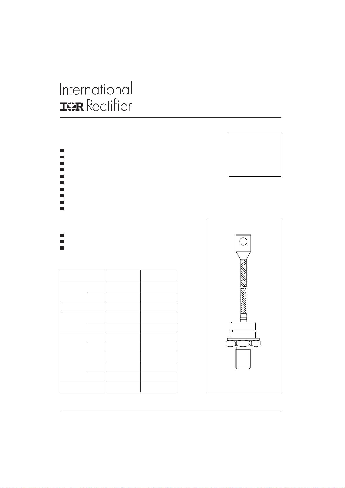
Stud version JEDEC DO-30
Maximum junction temperature 125°C
Typical Applications
Snubber diode for GTO
High voltage free-wheeling diode
Fast recovery rectifier applications
1 10A
Major Ratings and Characteristics
Parameters SD103N/R Units
I
F(AV)
@ T
C
I
F(RMS)
I
FSM
I2t@
V
RRM
trrrange 1.0 to 2.0 µs
T
J
@ 50Hz 3570 A
@ 60Hz 3730 A
50Hz 64 KA2s
@ 60Hz 58 KA
range 400 to 2500 V
@ T
J
www.irf.com
110 A
85 °C
173 A
25 °C
- 40 to 125 °C
2
s
case style
DO-205AC (DO-30)
1
SD103N/R Series
Bulletin I2062 rev. B 12/96
ELECTRICAL SPECIFICATIONS
Voltage Ratings
Voltage V
Type number Code peak and off-state voltage repetitive peak voltage T
04 400 500
SD103N/R..S10 08 800 900
10 1000 1100
12 1200 1300
SD103N/R..S15 14 1400 1500
16 1600 1700
SD103N/R..S20
20 2000 2100
25 2500 2600
Forward Conduction
Parameter SD103N/R Units Conditions
I
Max. average forward current 110 A 180° conduction, half sine wave.
F(AV)
@ Case temperature 85 °C
I
Max. RMS current 173 A DC @ 75°C case temperature
F(RMS)
Max. peak, one-cycle 3570 t = 10ms No voltage
I
FSM
non-repetitive forward current 3730 t = 8.3ms reapplied
2
t Maximum I2t for fusing 64 t = 10ms No voltage Initial TJ = TJ max.
I
2
I
√t Maximum I2√t for fusing 636 KA2√s t = 0.1 to 10ms, no voltage reapplied
V
Low level of threshold voltage 1.36 (16.7% x π x I
F(TO)1
High level of threshold voltage 1.94 (I > π x I
V
F(TO)2
r
Low level of forward slope resistance 2.55 (16.7% x π x I
f1
r
High level of forward slope resistance 1.11 (I > π x I
f2
V
Max. forward voltage 2.23 V Ipk= 345A, TJ = 25°C, tp = 400 µs square pulse
FM
max. repetitive V
RRM
, maximum non- I
RSM
VVmA
3000 t = 10ms 100% V
3140 t = 8.3ms reapplied Sinusoidal half wave,
58 t = 8.3ms reapplied
45 t = 10ms 100% V
41 t = 8.3ms reapplied
A
KA2s
V
mΩ
F(AV)
), TJ = TJ max.
F(AV)
F(AV)
), TJ = TJ max.
F(AV)
RRM
RRM
< I < π x I
< I < π x I
), TJ = TJ max.
F(AV)
), TJ = TJ max.
F(AV)
max.
RRM
= 125°C
J
35
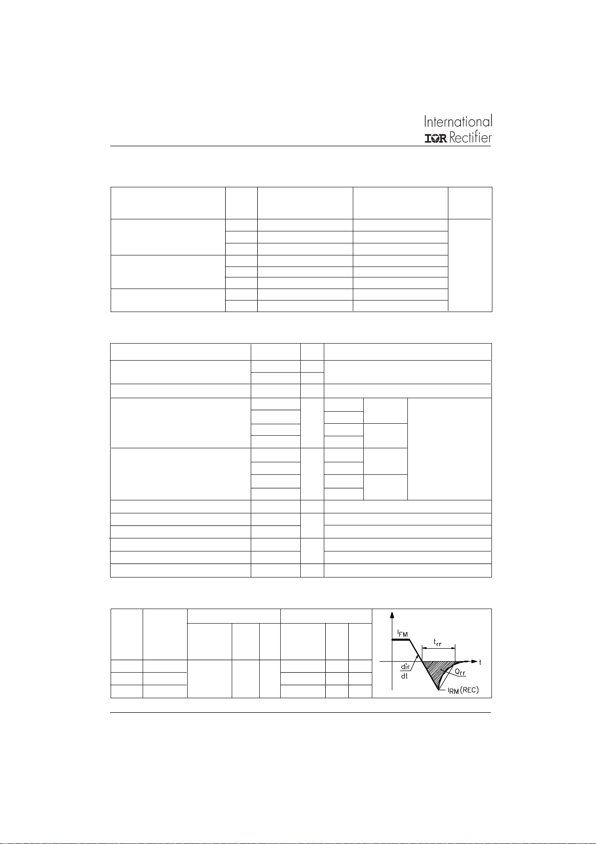
Recovery Characteristics
Code
T
= 25 oC
J
typical t
@ 25% I
rr
RRM
Test conditions Max. values @ T
I
pk
Square Pulse @ 25% I
di/dt V
r
t
rr
(µs) (A) (A/µs) (V) (µs) (µC) (A)
S10 1.0 1.6 21 27
S15 1.5 350 25 -30 2.3 61 37
S20 2.0 3.2 75 3 9
J
QrrI
RRM
2
= 125 °C
rr
www.irf.com
SD103N/R Series
Bulletin I2062 rev. B 12/96
Thermal and Mechanical Specification
Parameter SD103N/R Units Conditions
T
Max. operating temperature range -40 to 125
J
Max. storage temperature range -40 to 150
T
stg
Max. thermal resistance, junction to case 0.16 DC operation
R
thJC
Max. thermal resistance, case to heatsink 0.10 Mounting surface, smooth, flat and greased
R
thCS
T Mounting torque ± 10% 15.5 Not lubricated threads
13.5 Lubricated threads
wt Approximate weight 120 g
Case style DO-205AC(DO-30) See Outline Table
∆R
Conduction
thJC
(The following table shows the increment of thermal resistence R
Conduction angle Sinusoidal conduction Rectangular conduction Units Conditions
180° 0.011 0.012 T
120° 0.016 0.019
90° 0.021 0.023 K/ W
60° 0.029 0.030
30° 0.041 0.041
°C
K/W
Nm
when devices operate at different conduction angles than DC)
thJC
= TJ max.
J
Ordering Information Table
1 - Diode
2 - Essential part number
3 - 3 = Fast recovery
4 - N = Stud Normal Polarity (Cathode to Stud)
R = Stud Reverse Polarity (Anode to Stud)
5 - Voltage code: Code x 100 = V
6 -trr code (see Recovery Characteristics table)
7 - P = Stud base DO-205AC (DO-30) 1/2" 20UNF-2A
M = Stud base DO-205AC (DO-30) M12 X 1.75
8 -7 B = Flag top terminals (for Cathode/ Anode Leads)
S = Isolated lead with silicone sleeve
(Red = Reverse Polarity; Blue = Normal Polarity)
None = Not isolated lead
9 - C = Ceramic housing (over 1600V)
V = Glass-metal seal (only up to 1600V)
Device Code
SD 10 3 R 25 S20 P B C
4
(see Voltage Ratings table)
RRM
51 2 3
7
6 89
www.irf.com
3

SD103N/R Series
.
.
Bulletin I2062 rev. B 12/96
Outline Table
CERAMIC HOUSING
16.5 (0.65)
MAX.
6.5 (0.26) MIN.
2.6 (0.10) MAX
MAX.
35 (1.38)
DIA. 8.5 (0.33) NOM.
157 (6.18)
170 (6. 69 )
55 (2.16) MIN.
29 (1.14)
21 (0.82)
DIA. 22.5 (0.88) MAX.
MAX.
MAX.
12.5 (0.49)
MAX.
C.S. 16mm
2
(0.015 s.i.)
SW 27
Conforms to JEDEC DO-205AC (DO-30)
1/2"-20UNF-2A*
* FOR METRIC DEVICE: M12 X 1.75
GLASS-METAL SEAL
157 (6.18)
170 ( 6.69)
DIA. 8.5 (0.33) NOM.
All dimensions in millimeters (inches)
16.5 (0.65)
MAX.
MAX.
35 (1.38)
6.5 (0.26) MIN.
C.S. 16mm
(0.015 s.i.)
2.6 (0.10) MAX
2
DIA. 23.5 (0.93) MAX.
4
55 (2.1 6) MIN.
MAX.
24 (0.94)
MAX.
21 (0.82)
MAX.
12.5 (0.49)
1/2"-20UNF-2A*
* FOR METRIC DEVICE: M12 X 1.75
SW 27
www.irf.com

Outline Table
CERAMIC HOUSING
SD103N/R Series
Bulletin I2062 rev. B 12/96
16.5 (0.65)
DIA. 22.5 (0.88) MAX.
45 (1.77)
MAX.
29 (1.14)
MAX.
21 ( 0. 8 2)
*FOR METRIC DEVICE. M12 X 1.75
12.5 (0.49)
MAX.
1/2"-20UNF-2A*
27 (1.06)
5.6 (0.22)
DIA. 5.54 (0.22)
9.5 (0.37)
2.4 (0.09)
40.5 (1.59) MAX.
GLASS-METAL SEAL
DO-205AC (DO-30) Flag
All dimensions in millimeters (inches)
16.5 (0.65)
5.6 (0.22)
DIA. 5.54 (0.22)
www.irf.com
DIA. 23.5 (0.93) MAX.
41 (1.61) MAX.
MAX.
24 (0.94)
MAX.
12.5 (0.49)
MAX.
21 (0.82)
*FOR METRIC DEVICE. M12 X 1.75
27 (1.06)
9.5 (0.37)
36.5 (1.44)
1/2"-20UNF-2A*
2.4 (0.09)
5

SD103N/R Series
Bulletin I2062 rev. B 12/96
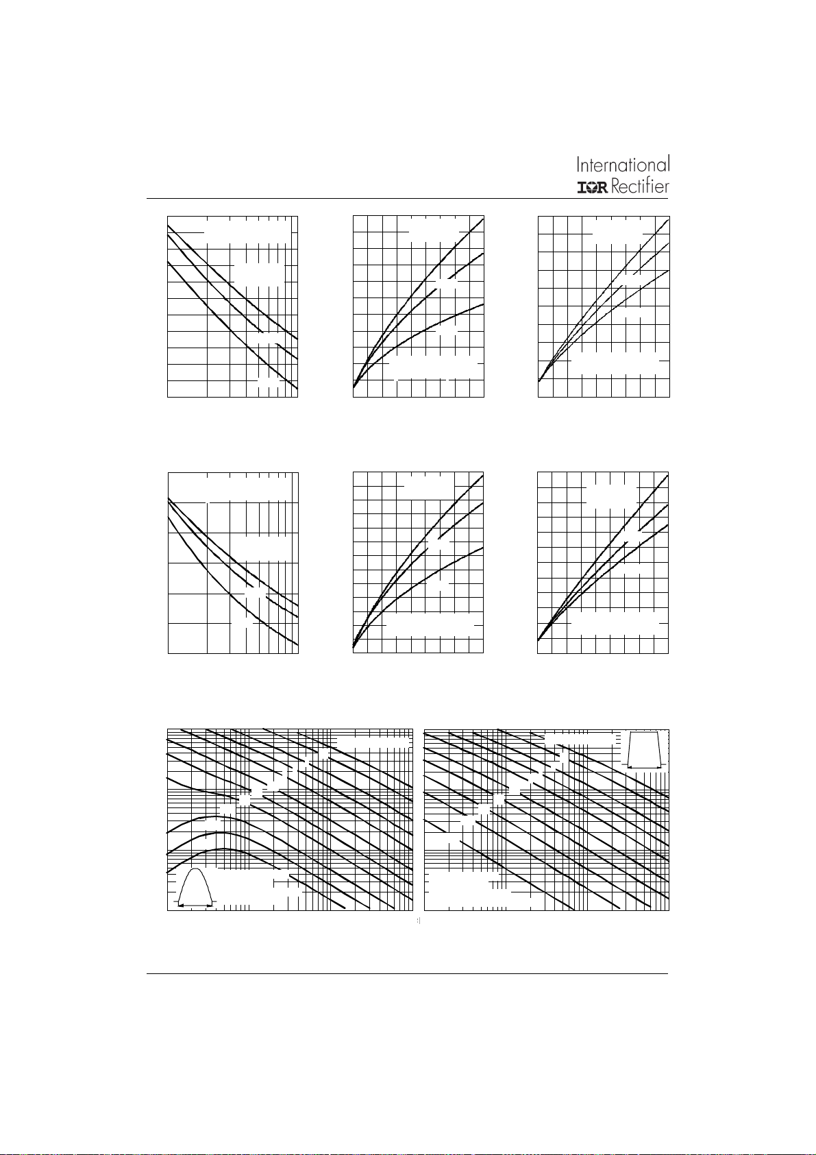
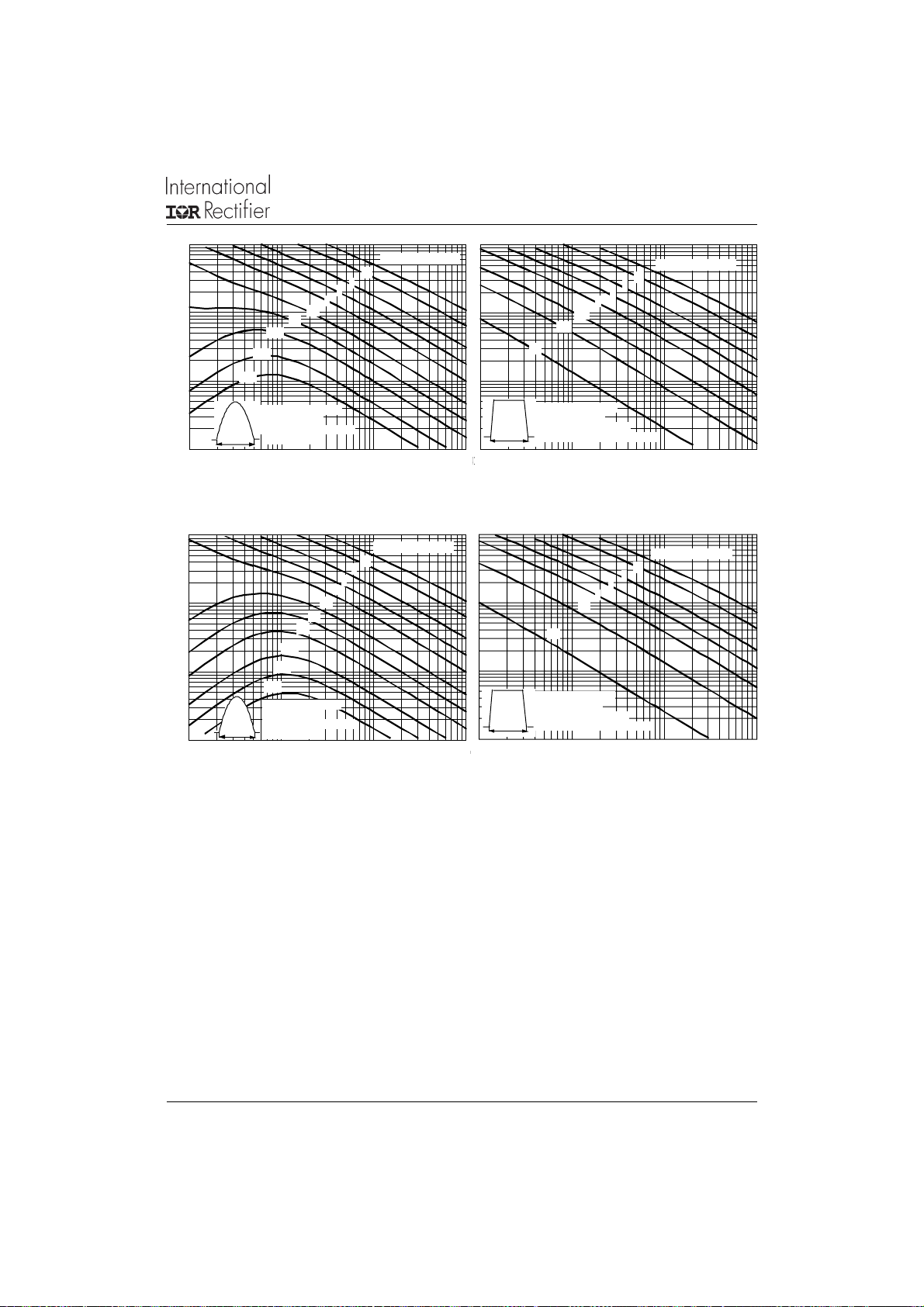
130
120
110
SD103N/R Se ries
R (DC) = 0.16 K/W
thJC
Conduction Angle
100
90
80
70
60
Maximum Allowable Case Temperature (°C)
0 20406080100120
30°
60°
90°
120°
180°
Average Forward Current (A)
Fig. 1 - Current Ratings Characteristics Fig. 2 - Current Ratings Characteristics
280
240
200
160
120
80
40
0
Maximum Average Forward Power Loss (W)
180°
120°
90°
60°
30°
SD103N/R Series
T = 125°C
0 20 40 60 80 100 120
Av er ag e Fo rwar d Cu rren t (A )
Fig. 3 - Forward Power Loss Characteristics Fig. 4 - Forward Power Loss Characteristics
RMS Limit
Conduction An g le
J
130
120
SD103N/R Se r ies
R (DC) = 0.16 K/W
thJC
110
100
90
30°
80
70
60
Maximum Allowable Case Temperature (°C)
0 20 40 60 80 100 120 140 160 180
Conduction Period
60°
90°
120°
Average Forward Current (A)
450
400
350
300
250
200
150
DC
180°
120°
90°
60°
30°
RMS Limit
100
50
0
Maximum Average Forward Power Loss (W)
0 20 40 60 80 100 120 140 160 180
Average Forward Current (A)
180°
DC
Conduction P eri od
SD103N/R Se ries
T = 125°C
J
3500
At Any Rated Load Condition And With
Rated V Applied Following Surge.
3000
2500
2000
1500
1000
Peak Half Sine Wave Forward Current (A)
500
1 10 100
Number Of Equal Amplitu de Half Cycle C urr ent Pulses (N)
Fig. 5 - Maximum Non-repetitive Surge Current Fig. 6 - Maximum Non-repetitive Surge Current
RRM
SD103N/R Series
Init ia l T = 125 °C
J
@ 60 Hz 0.0083 s
@ 50 Hz 0.0100 s
6
4500
Maximum Non Repetitive Surge Current
4000
3500
3000
Versus Pulse Train Duration.
Initi a l T = 125 °C
No Voltage Reapplied
Rated V Reapplied
RRM
2500
2000
1500
1000
SD103N/R Se ries
Peak Half Sine Wave Forward Current (A)
500
0.01 0.1 1
Pulse Train Duration (s)
www.irf.com
J

SD103N/R Series
Bulletin I2062 rev. B 12/96
1000
1000
100
100
10
10
SD103N/R Se ries
T = 25 °C
J
T = 125 °C
J
1
Steady State Value:
R = 0.16 K/W
(DC Operation)
thJC
0.1
0.01
thJC
Instantaneous Forward Current (A)
1
1
0 .5 11.522.533.54
0.511.522.533.54
Instantaneous Forward Voltage (V)
Trans ie n t Th e rmal Impeda nce Z (K/W)
0.001
0.001 0.01 0.1 1 10
Square Wave Pulse Duration (s)
Fig. 7 - Forward Voltage Drop Characteristics Fig. 8 - Thermal Impedance Z
140
120
V
FP
I
T = 125°C
J
100
80
60
40
Forward Recovery (V)
20
T = 25°C
J
SD103N/ R.. S20 S er i es
SD103N/R Se r ies
Characteristic
thJC
0
0 200 400 600 800 1000 1200 1400 1600 1800 2000
1.8
1.6
1.4
Maximum Reverse Recovery Time - Trr (µs)
1.2
Rate Of Fall Of Forward Current - di/dt (A/µs)
SD103N/R..S10 Series
T = 125 °C; V = 30V
J
r
I = 350 A
FM
Square Pulse
200 A
100 A
10 100
www.irf.com
Rate Of Rise Of Forward Current di/dt (A/usec)
Fig. 9 - Typical Forward Recovery Characteristics
60
I = 350 A
FM
50
40
30
20
10
10 20 30 40 50 60 70 80 90100
Maximum Reverse Recovery Charge - Qrr (µC)
Rate Of Fall Of Forward Current - di/dt (A/µs)
Square Pulse
200 A
100 A
SD103N/R..S10 Series
T = 125 °C; V = 30V
J
r
90
I = 350 A
80
FM
Square Pulse
70
60
200 A
50
40
100 A
30
20
10
Maximu m Re verse R ecovery Cu rrent - Ir r (A)
Rate Of Fall Of Forward Current - di/dt (A/µs)
SD103N/R..S10 Se ries
T = 125 °C; V = 30V
J
r
10 20 30 40 50 60 70 80 90 100
Fig. 11 - Recovery Charge CharacteristicsFig. 10 - Recovery Time Characteristics Fig. 12 - Recovery Current Characteristics
7
SD103N/R Series
4
Bulletin I2062 rev. B 12/96
2.7
2.6
2.5
2.4
2.3
SD103N/R..S15 Series
T = 125 °C; V = 30V
J
r
I = 350 A
FM
Square Pulse
2.2
2.1
2
1.9
200 A
1.8
1.7
Maximum R everse Rec overy Time - Trr (µs)
1.6
10 100
Rate Of Fall Of Forward Current - di/dt (A/µs)
100 A
Fig. 13 - Recovery Time Characteristics
4.5
4
3.5
3
2.5
2
Maximum Reverse Recovery Time - Trr (µs)
1.5
Rate Of Fall Of Forward Current - di/dt (A/µs)
SD103N/R..S20 Seri es
T = 125 °C; V = 30V
J
r
I = 350 A
FM
Square Pulse
200 A
100 A
10 100
140
130
I = 350 A
FM
Sq u a re Pul se
120
110
100
200 A
90
80
70
100 A
60
50
40
30
10 20 30 40 50 60 70 80 90100
Maximum Reverse Recovery Charge - Qrr (µC)
Rate Of Fall Of Forward Current - di/dt (A/µs)
SD103N/R..S15 Se ries
T = 125 °C; V = 30 V
J
r
110
100
I = 350 A
FM
Square Pulse
90
80
70
60
200 A
100 A
50
40
30
20
10
Maximum Reverse Recovery Current - Irr (A)
Rate Of Fall Of Forward Current - di/dt (A/µs)
SD103N/R..S15 Se ries
T = 125 °C; V = 30 V
J
r
10 20 30 40 50 60 70 80 90 100
Fig. 14 - Recovery Charge Characteristics Fig. 15 - Recovery Current Characteristics
170
160
150
I = 350 A
FM
Square Pulse
140
130
120
200 A
110
100
90
100 A
80
70
60
50
40
Maximum Reverse Recovery Charge - Qrr (µC)
Rate Of Fall Of Forward Current - di/dt (A/µs)
SD103N/R..S20 Series
T = 125 °C; V = 30V
J r
10 20 30 40 50 60 70 80 90100
130
120
110
I = 350 A
FM
Square Pulse
100
90
200 A
80
70
60
100 A
50
40
30
20
10
Maximum Reverse Recovery Current - Irr (A)
Rate Of Fall Of Forward Current - di/dt (A/µs)
SD103N/R..S20 Series
T = 125 °C; V = 30V
J r
10 20 30 40 50 60 70 80 90100
Fig. 16 - Recovery Time Characteristics Fig. 17 - Recovery Charge Characteristics Fig. 18 - Recovery Current Characteristics
1E4
20 joules pe r puls e
10
4
2
1
1E3
0.04
0.02
1E2
Peak Forward Current (A)
1E1
0.01
SD103N/R..S10 Series
Sinusoidal Pulse
T = 125°C, V = 1120 V
J
dv/dt=1000V/µs
tp
1E1 1E2 1E 3 1E
0.4
0.2
0.1
RRM
Puls e Base width (µs)
Fig. 19 - Maximum Total Energy Loss Per Pulse Characteristics
8
20 joules per pulse
10
4
2
1
0.4
0.2
0.1
0.06
0.04
SD103N/R..S10 Series
Trapezoidal Pulse
T = 125°C, V = 1120V
dv/dt=1000V/µs, di/dt=50A/µs
1E1
1E4
E1 1E2 1E3 1E4
RRM
J
Pu ls e Basewid th (µs)
www.irf.com
tp
SD103N/R Series
4
4
Bulletin I2062 rev. B 12/96
1E4
20 joules per pulse
10
4
2
1
1E3
0.02
1E2
0.01
Peak Forward Current (A)
1E1
1E1 1E2 1E3 1E
tp
0.4
0.2
0.04
SD103N/R. .S1 5 Series
Sinusoidal Pulse
T = 125°C, V = 1120V
dv/dt=1000V/µs
RRM
J
Pu ls e Basewid th (µs)
Fig. 20 - Maximum Total Energy Loss Per Pulse Characteristics
1E4
1E3
1E2
Peak Forward Current (A)
1E1
1E1 1E 2 1E 3 1E
0.01
SD103N/R..S20 Series
Sinusoid al Pulse
T = 125°C, V = 1760V
J
tp
dv/dt=1000V/µs
0.4
0.2
0.1
0.04
0.02
RRM
10
4
2
1
20 joules per pu lse
Pu ls e Basewid th (µs)
Fig. 21 - Maximum Total Energy Loss Per Pulse Characteristics
20 joules per pulse
10
4
2
1
0.4
0.2
0.1
SD103N/R..S15 Series
Trapezoi da l Pulse
T = 125°C, V = 1120V
tp
dv/dt=1000V/µs, di/dt=50A/µs
1E1
1E4
E1 1E2 1E3 1E4
RRM
J
Puls e Base wid th (µs)
20 joules per pulse
10
4
2
1
0.4
0.2
SD103N/R..S20 Series
Tra pe z oi d a l Pul se
T = 125°C, V = 1760V
tp
dv/dt =10 00V/ µ s , di/dt=50 A/ µ s
1E1
1E1 1E2 1E3 1E4
1E4
RRM
J
Pulse Basewidth (µs)
www.irf.com
9
 Loading...