Vishay SD103AW, SD103BW, SD103CW Schematic [ru]

www.vishay.com
Small Signal Schottky Diodes
MECHANICAL DATA
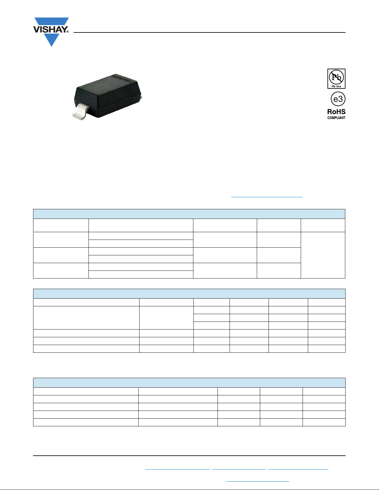
Case: SOD-123
Weight: approx. 10.3 mg
Cathode band color: black
Packaging codes/options:
18/10K per 13" reel (8 mm tape), 10K/box
08/3K per 7" reel (8 mm tape), 15K/box
SD103AW, SD103BW, SD103CW
Vishay Semiconductors
FEATURES
• The low forward voltage drop and fast switching
make it ideal for protection of MOS devices,
steering, biasing, and coupling diodes for fast
switching and low logic level applications
• Other applications are click suppression,
efficient full wave bridges in telephone subsets,
and blocking diodes in rechargeable low voltage
battery systems
• The SD103 series is a metal-on-silicon Schottky barrier
device which is protected by a PN junction guardring
• For general purpose applications
• AEC-Q101 qualified
• Base P/N-E3 - RoHS-compliant, commercial grade
• Base P/N-HE3 - RoHS-compliant, AEC-Q101 qualified
• Material categorization: For definitions of compliance
please see www.vishay.com/doc?99912
PARTS TABLE
PART ORDERING CODE
SD103AW
SD103BW
SD103CW
ABSOLUTE MAXIMUM RATINGS (T
PARAMETER TEST CONDITION PART SYMBOL VALUE UNIT
Repetitive peak reverse voltage
Forward continuous current
Power dissipation (infinite heat sink)
Single cycle surge 10 μs square wave I
Note
(1)
Valid provided that electrodes are kept at ambient temperature
THERMAL CHARACTERISTICS (T
PARAMETER TEST CONDITION SYMBOL VALUE UNIT
Thermal resistance junction to ambient air
Junction temperature T
Operating temperature range T
Storage temperature range T
Note
(1)
Valid provided that electrodes are kept at ambient temperature
SD103AW-E3-08 or SD103AW-E3-18
SD103AW-HE3-08 or SD103AW-HE3-18
SD103BW-E3-08 or SD103BW-E3-18
SD103BW-HE3-08 or SD103BW-HE3-18
SD103CW-E3-08 or SD103CW-E3-18
SD103CW-HE3-08 or SD103CW-HE3-18
= 25 °C, unless otherwise specified)
amb
(1)
(1)
= 25 °C, unless otherwise specified)
amb
(1)
INTERNAL
CONSTRUCTION
Single diode S6
Single diode S7
Single diode S8
SD103AW V
SD103BW V
SD103CW V
RRM
RRM
RRM
I
F
P
tot
FSM
R
thJA
j
op
stg
TYPE MARKING REMARKS
Tape and reel
40 V
30 V
20 V
350 mA
400 mW
2A
300 K/W
125 °C
- 55 to + 125 °C
- 55 to + 150 °C
Rev. 1.6, 11-Mar-13
For technical questions within your region: DiodesAmericas@vishay.com
THIS DOCUMENT IS SUBJECT TO CHANGE WITHOUT NOTICE. THE PRODUCTS DESCRIBED HEREIN AND THIS DOCUMENT
ARE SUBJECT TO SPECIFIC DISCLAIMERS, SET FORTH AT www.vishay.com/doc?91000
1
, DiodesAsia@vishay.com, DiodesEurope@vishay.com
Document Number: 85681

www.vishay.com
18488
0.01
1000
100
0.1
1
10
0 0.4 0.6 0.8 1.00.2
I - Forward Current (mA)
F
VF- Forward Voltage (V)
18489
4
5
3
2
0
1
0.5 1.001.5
I - Forward Current (A)
F
VF- Forward Voltage (V)
duty cycle = 2 %
t
p
= 300 ms
SD103AW, SD103BW, SD103CW
Vishay Semiconductors
ELECTRICAL CHARACTERISTICS (T
= 25 °C, unless otherwise specified)
amb
PARAMETER TEST CONDITION PART SYMBOL MIN. TYP. MAX. UNIT
V
Leakage current
Forward voltage drop
Diode capacitance V
I
= IR = 50 mA to 200 mA,
Reverse recovery time
F
TYPICAL CHARACTERISTICS (T
= 30 V SD103AW I
R
V
= 20 V SD103BW I
R
V
= 10 V SD103CW I
R
I
= 20 mA V
F
I
= 200 mA V
F
= 0 V, f = 1 MHz C
R
recover to 0.1 I
= 25 °C, unless otherwise specified)
amb
R
R
R
R
F
F
D
t
rr
1000
100
10
1
- Reverse Current (µA)
0.1
R
I
0.01
0 5 10 15 20 25 30 35 40 45 50
20084
V - Reverse Voltage (V)
R
50 pF
10 ns
= 125 °C
T
amb
100 °C
75 °C
50 °C
25 °C
5μA
5μA
5μA
370 mV
600 mV
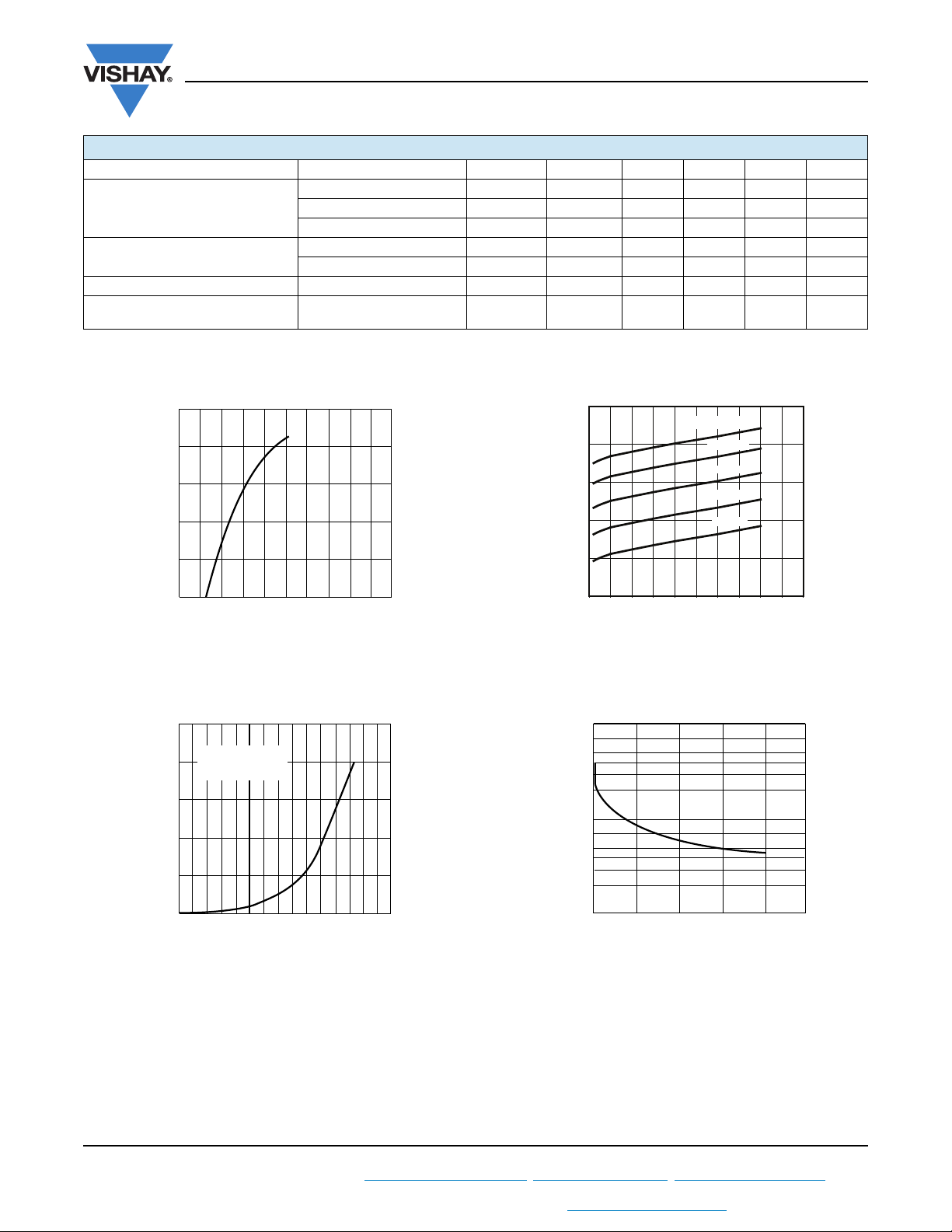
Fig. 1 - Typical Variation of Forward Current vs. Forward Voltage
Fig. 2 - Typical High Current Forward Conduction Curve
Fig. 3 - Typical Variation of Reverse Current at Various
Temperatures
100
10
D
C- Diode Capacitance (pF)
1
10 20 30 40 050
18491
V R - Reverse Voltag e (V)
Fig. 4 - Typical Capacitance vs. Reverse Voltage
Rev. 1.6, 11-Mar-13
2
For technical questions within your region: DiodesAmericas@vishay.com
, DiodesAsia@vishay.com, DiodesEurope@vishay.com
Document Number: 85681
THIS DOCUMENT IS SUBJECT TO CHANGE WITHOUT NOTICE. THE PRODUCTS DESCRIBED HEREIN AND THIS DOCUMENT
ARE SUBJECT TO SPECIFIC DISCLAIMERS, SET FORTH AT www.vishay.com/doc?91000
 Loading...