VISHAY SD103AW-V, SD103BW-V, SD103CW-V Technical data

SD103AW-V/103BW-V/103CW-V
Vishay Semiconductors
Small Signal Schottky Diodes
Features
• The low forward voltage drop and fast
switching make it ideal for protection of
MOS devices, steering, biasing, and coupling diodes for fast switching and low
logic level applications.
• Other applications are click suppression, efficient
full wave bridges in telephone subsets, and blocking diodes in rechargeable low voltage battery systems.
• The SD103 series is a metal-on-silicon Schottky
barrier device which is protected by a PN junction
guard ring.
• This diode is also available in the MiniMELF case
with the type designations LL103A to LL103C,
DO35 case with the type designations SD103A to
SD103C and SOD323 case with type designations
SD103AWS-V to SD103CWS-V.
• For general purpose applications.
• Lead (Pb)-free component
• Component in accordance to RoHS 2002/95/EC
and WEEE 2002/96/EC
Parts Table
Par t Ordering code Type Marking Remarks
SD103AW-V SD103AW-V-GS18 or SD103AW-V-GS08 S6 Tape and Reel
SD103BW-V SD103BW-V-GS18 or SD103BW-V-GS08 S7 Tape and Reel
SD103CW-V SD103CW-V-GS18 or SD103CW-V-GS08 S8 Tape and Reel
e3
17431
Mechanical Data
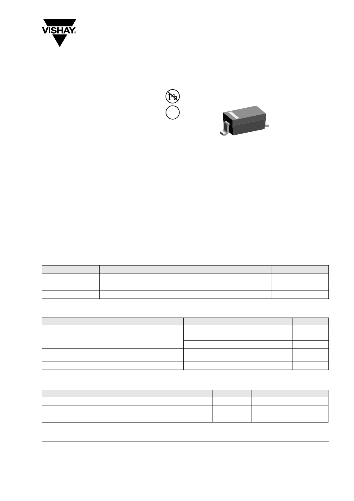
Case: SOD123 Plastic case
Weight: approx. 10.3 mg
Packaging Codes/Options:
GS18/10 k per 13" reel (8 mm tape), 10 k/box
GS08/3 k per 7" reel (8 mm tape), 15 k/box
Absolute Maximum Ratings
T
= 25 °C, unless otherwise specified
amb
Parameter Test condition Part Symbol Val ue Unit
Peak reverse voltage
Power dissipation
(Infinite heat sink)
Single cycle surge 10 µs square wave
SD103AW-V
SD103BW-V
SD103CW-V
Thermal Characteristics
T
= 25 °C, unless otherwise specified
amb
Para me te r Test condition Symbol Val ue Unit
Thermal resistance junction to ambient air R
Junction temperature
Storage temperature range
1)
Valid provided that electrodes are kept at ambient temperature
Document Number 85681
Rev. 1.4, 18-Sep-06
T
V
V
V
thJA
T
stg
RRM
RRM
RRM
P
I
FSM
j
40 V
30 V
20 V
tot
- 55 to + 150
1)
400
2A
1)
300
1)
125
1)
mW
K/W
°C
°C
www.vishay.com
1

SD103AW-V/103BW-V/103CW-V
Vishay Semiconductors
Electrical Characteristics
T
= 25 °C, unless otherwise specified
amb
Parameter Test condition Par t Symbol Min Ty p. Max Unit
Leakage current V
Forward voltage drop I
Diode capacitance V
Reverse recovery time I
Typical Characteristics
T
= 25 °C, unless otherwise specified
amb
= 30 V
R
= 20 V
V
R
= 10 V
V
R
= 20 mA V
F
= 200 mA V
I
F
= 0 V, f = 1 MHz C
R
= IR = 50 mA to 200 mA,
F
recover to 0.1 I
R
SD103AW-V
SD103BW-V
SD103CW-V
I
R
I
R
I
R
F
F
D
t
rr
50 pF
10 ns
5µA
5µA
5µA
370 mV
600 mV
1000
100
10
1
F
0.1
I - Forward Current (mA)
0.01
0 0.4 0.6 0.8 1.00.2
18488
VF- Forward Voltage (V)
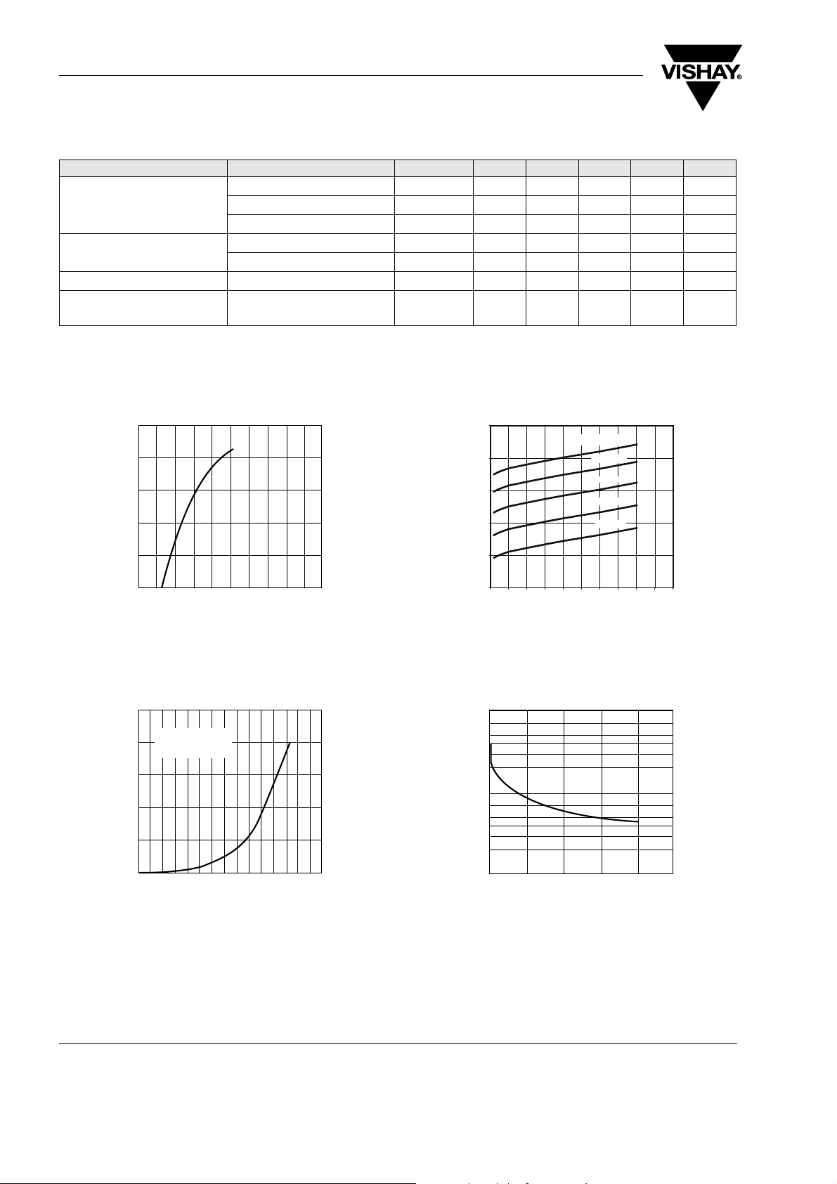
Figure 1. Typical Variation of Forward Current vs. Forward Voltage
5
t
= 300 ms
p
4
duty cycle = 2 %
3
2
1000
= 125 °C
T
amb
100
10
1
- Reverse Current (µA)
0.1
R
I
0.01
0 5 10 15 20 25 30 35 40 45 50
20084
V - Reverse Voltage (V)
R
100 °C
75 °C
50 °C
25 °C
Figure 3. Typical Variation of Reverse Current at Various
Temperatures
100
10
F
1
I - Forward Current (A)
0
18489
0.5 1.00 1.5
VF- Forward Voltage (V)
Figure 2. Typical High Current Forward Conduction Curve
www.vishay.com
2
D
C- Diode Capacitance (pF)
1
10 20 30 40 050
18491
V R - Reverse Voltag e (V)
Figure 4. Typical Capacitance vs. Reverse Voltage
Document Number 85681
Rev. 1.4, 18-Sep-06
 Loading...