

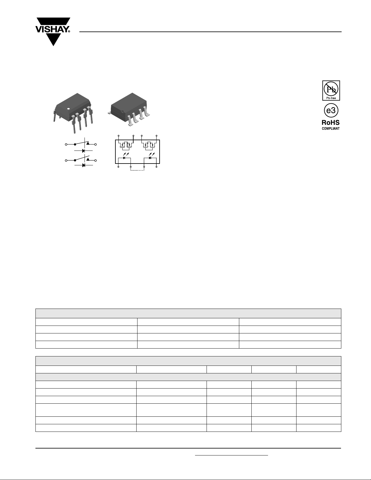
DIP
S1 S1'
S2
i179032
LH1502BAC, LH1502BACTR, LH1502BB
Vishay Semiconductors
Dual 1 Form A/B, C Solid State Relay
FEATURES
SMD
S2'S2S1 S1'
8 76 5
S2'
1234
• Current limit protection
• Isolation test voltage 3750 V
• Typical RON 20 Ω
• Load voltage 350 V
• Load current 150 mA
• High surge capability
• Clean bounce free switching
• Low power consumption
• SMD lead available on tape and reel
• Lead (Pb)-free component
• Component in accordance to RoHS 2002/95/EC and
WEEE 2002/96/EC
RMS
DESCRIPTION
The LH1502 relays contain normally open and normally
closed switches that can be used independently as a 1 form
A and 1 form B relay, or when used together, as a 1 form C
relay. The relays are constructed as a multi-chip hybrid
device. Actuation control is via an infrared LED. The output
switch is a combination of a photodiode array with MOSFET
switches and control circuity.
APPLICATIONS
• General telecom switching
- On/off hook control
- Ring delay
- Dial pulse
- Ground start
- Ground fault protection
• Instrumentation
• Industrial controls
AGENCY APPROVALS
UL1577: file no. E52744 system code H or J, double
CSA: certification 093751
protection
ORDER INFORMATION
PART REMARKS PACKAGE
LH1502BAC Tubes SMD-8
LH1502BACTR Tape and reel SMD-8
LH1502BB Tubes DIP-8
ABSOLUTE MAXIMUM RATINGS
PARAMETER TEST CONDITION SYMBOL VALUE UNIT
SSR
LED continuous forward current I
LED reverse voltage I
DC or peak AC load voltage I
Continuous DC load current
(form C operation)
Peak load current, form A t = 100 ms I
Peak load current (single shot), form B I
(1)
≤ 10 µA V
R
≤ 50 µA V
L
F
R
L
I
L
P
P
50 mA
8.0 V
350 V
150 mA
(4)
350 mA
Document Number: 83806 For technical questions, please contact: optocoupler.answers@vishay.com
Rev. 1.3, 08-May-08 73
www.vishay.com
LH1502BAC, LH1502BACTR, LH1502BB
Vishay Semiconductors
ABSOLUTE MAXIMUM RATINGS
Dual 1 Form A/B, C Solid State Relay
(1)
PARAMETER TEST CONDITION SYMBOL VALUE UNIT
SSR
Ambient operating temperature range T
Storage temperature range T
Pin soldering temperature
Input to output isolation test voltage t = 1.0 s, I
Pole-to-pole isolation voltage (S1 to S2)
(2)
(3)
,
t = 10 s max. T
= 10 µA max. V
ISo
(dry air, dust free, at sea level)
Output power dissipation (continuous) P
amb
stg
sld
ISO
diss
- 40 to + 85 °C
- 40 to + 125 °C
260 °C
3750 V
RMS
1600 V
600 mW
Notes
(1)
T
= 25 °C, unless otherwise specified.
amb
Stresses in excess of the absolute maximum ratings can cause permanent damage to the device. Functional operation of the device is not
implied at these or any other conditions in excess of those given in the operational sections of this document. Exposure to absolute maximum
ratings for extended periods of the time can adversely affect reliability.
(2)
Refer to reflow profile for soldering conditions for surface mounted devices (SMD). Refer to wave profile for soldering conditions for through
hole devices (DIP).
(3)
Breakdown occurs between the output pins external to the package.
(4)
Refer to current limit performance application note for a discussion on relay operation during transient currents.
ELECTRICAL CHARACTERISTICS
PARAMETER TEST CONDITION SYMBOL MIN. TYP. MAX. UNIT
INPUT
LED forward current, switch turn-on (NO) I
LED forward current, switch turn-off (NO) V
LED forward current, switch turn-on (NC) I
LED forward current, switch turn-off (NC) V
LED forward voltage I
OUTPUT
On-resistance (NO, NC)
Off-resistance (NO) I
Off-resistance (NC) I
Current limit (NO) I
Off-state leakage current (NO) I
Off-state leakage current (NC) I
Off-state leakage current (NO, NC)
Output capacitance (NO) I
Output capacitance (NC) I
TRANSFER
Capacitance (input to output) V
Turn-on time (NO)
Turn-on time (NC)
Turn-off time (NO)
Turn-off time (NC)
Note
= 25 °C, unless otherwise specified.
T
amb
Minimum and maximum values are testing requirements. Typical values are characteristics of the device and are the result of engineering
evaluation. Typical values are for information only and are not part of the testing requirements.
www.vishay.com For technical questions, please contact: optocoupler.answers@vishay.com
74 Rev. 1.3, 08-May-08
= 100 mA, t = 10 ms I
L
= ± 300 V I
L
= 300 mA, t = 10 ms I
L
= ± 300 V I
L
= 10 mA V
F
I
= 5.0 mA (NO), IF = 0 mA (NC),
F
I
= 50 mA (NC)
L
= 0 mA, VL = ± 100 V R
F
= 5.0 mA, VL = ± 100 V R
F
= 5.0 mA, t = 5.0 ms, VL = ± 5.0 V I
F
= 0 mA, VL = ± 100 V I
F
= 5.0 mA, VL = ± 100 V I
F
I
= 0 mA (NO), IF = 5.0 mA (NC),
F
V
= ± 200 V
L
= 0 mA, VL = 50 V C
F
= 5.0 mA, VL = 50 V C
F
= 1.0 V C
ISO
I
= 10 mA, IL = 37.5 mA,
F
V
= 150 V
L
I
= 10 mA, IL = 37.5 mA,
F
V
= 150 V
L
I
= 10 mA, IL = 37.5 mA,
F
V
= 150 V
L
I
= 10 mA, IL = 37.5 mA,
F
V
= 150 V
L
R
Fon
Foff
Fon
Foff
ON
OFF
OFF
LMT
O
O
I
O
t
on
t
on
t
off
t
off
0.6 2.0 mA
0.4 0.5 mA
0.2 0.9 mA
1.0 2.0 mA
F
1.15 1.26 1.45 V
12 20 25 Ω
0.35 5000 GΩ
0.1 1.4 GΩ
270 290 380 mA
0.02 1000 nA
0.07 1.0 µA
1.0 µA
O
O
IO
50 pF
50 pF
3.0 pF
0.2 3.2 6.0 ms
0.2 3.8 6.0 ms
1.6 3.0 ms
0.8 3.0 ms
Document Number: 83806

LH1502BAC, LH1502BACTR, LH1502BB
Dual 1 Form A/B, C Solid State Relay
TYPICAL CHARACTERISTICS
T
= 25 °C, unless otherwise specified
amb
150
120
90
60
30
Load Current (mA)
0
Form A
- 40 - 20 0 20 40 60 80
ilh1502bb_00
Ambient Temperature (°C)
Fig. 1 - Recommended Operating Conditions Fig. 2 - Recommended Operating Conditions
PACKAGE DIMENSIONS in inches (millimeters)
DIP
5.0 mA
0.380 (9.65)
0.100 (2.54)
6 to 0.031 (6 to 0.80) dia.
Vishay Semiconductors
150
120
90
50
Load Current (mA)
30
0
Form B
- 40 - 20 0 20 40 60 80
ilh1502bb_01
Ambient Temperature (°C)
0.100 (2.54)
5.0 mA
0.250 (6.35)
i178017
SMD
0.018 (0.46)
0.318 (8.08)
ISO method A
0.380 (9.65)
0.100 (2.54)
0.018 (0.46)
0.318 (8.08)
0.360 (9.14)
0.375 (9.53)0.250 (6.35)
0.250 (6.35)
0.130 (3.30)
0.075 (1.90)
0.300 (7.62)
0.300 (7.62)
0.300 (7.62)
0.285 (7.24) typ.
0.360 (9.14) typ.
0.100 (2.54)
0.327 (8.31)
0.059 (1.50)
0.300 (7.62)
0.130 (3.30)
0.025 (0.64) typ.
0.010 (0.25) typ.
i178018
0.175 (4.45)
ISO method A
Document Number: 83806 For technical questions, please contact: optocoupler.answers@vishay.com
www.vishay.com
Rev. 1.3, 08-May-08 75

LH1502BAC, LH1502BACTR, LH1502BB
Vishay Semiconductors
Dual 1 Form A/B, C Solid State Relay
OZONE DEPLETING SUBSTANCES POLICY STATEMENT
It is the policy of Vishay Semiconductor GmbH to
1. Meet all present and future national and international statutory requirements.
2. Regularly and continuously improve the performance of our products, processes, distribution and operating systems with
respect to their impact on the health and safety of our employees and the public, as well as their impact on the environment.
It is particular concern to control or eliminate releases of those substances into the atmosphere which are known as ozone
depleting substances (ODSs).
The Montreal Protocol (1987) and its London Amendments (1990) intend to severely restrict the use of ODSs and forbid their use
within the next ten years. Various national and international initiatives are pressing for an earlier ban on these substances.
Vishay Semiconductor GmbH has been able to use its policy of continuous improvements to eliminate the use of ODSs listed in
the following documents.
1. Annex A, B and list of transitional substances of the Montreal Protocol and the London Amendments respectively.
2. Class I and II ozone depleting substances in the Clean Air Act Amendments of 1990 by the Environmental Protection Agency
(EPA) in the USA.
3. Council Decision 88/540/EEC and 91/690/EEC Annex A, B and C (transitional substances) respectively.
Vishay Semiconductor GmbH can certify that our semiconductors are not manufactured with ozone depleting substances and do
not contain such substances.
We reserve the right to make changes to improve technical design
and may do so without further notice.
Parameters can vary in different applications. All operating parameters must be validated for each customer application by the
customer. Should the buyer use Vishay Semiconductors products for any unintended or unauthorized application, the buyer shall
indemnify Vishay Semiconductors against all claims, costs, damages, and expenses, arising out of, directly or indirectly, any
claim of personal damage, injury or death associated with such unintended or unauthorized use.
Vishay Semiconductor GmbH, P.O.B. 3535, D-74025 Heilbronn, Germany
www.vishay.com For technical questions, please contact: optocoupler.answers@vishay.com
76 Rev. 1.3, 08-May-08
Document Number: 83806

Legal Disclaimer Notice
Vishay
Disclaimer
All product specifications and data are subject to change without notice.
Vishay Intertechnology, Inc., its affiliates, agents, and employees, and all persons acting on its or their behalf
(collectively, “Vishay”), disclaim any and all liability for any errors, inaccuracies or incompleteness contained herein
or in any other disclosure relating to any product.
Vishay disclaims any and all liability arising out of the use or application of any product described herein or of any
information provided herein to the maximum extent permitted by law. The product specifications do not expand or
otherwise modify Vishay’s terms and conditions of purchase, including but not limited to the warranty expressed
therein, which apply to these products.
No license, express or implied, by estoppel or otherwise, to any intellectual property rights is granted by this
document or by any conduct of Vishay.
The products shown herein are not designed for use in medical, life-saving, or life-sustaining applications unless
otherwise expressly indicated. Customers using or selling Vishay products not expressly indicated for use in such
applications do so entirely at their own risk and agree to fully indemnify Vishay for any damages arising or resulting
from such use or sale. Please contact authorized Vishay personnel to obtain written terms and conditions regarding
products designed for such applications.
Product names and markings noted herein may be trademarks of their respective owners.
Document Number: 91000 www.vishay.com
Revision: 18-Jul-08 1
 Loading...