VISHAY K3023PG, K3022P, K3021P, K3020PG, K3020P Datasheet
...
Optocoupler with Phototriac Output
Description
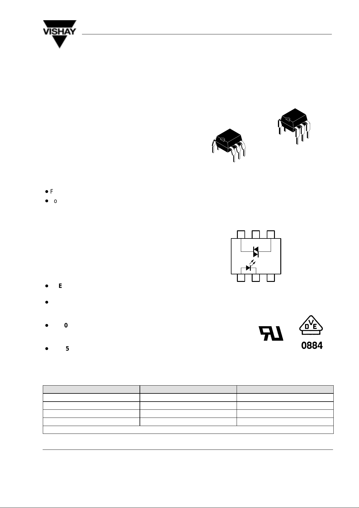
The K3020P(G) series consists of a phototransistor
optically coupled to a gallium arsenide infrared-emitting diode in a 6-lead plastic dual inline package. The
elements are mounted on one leadframe using a
coplanar technique, providing a fixed distance between input and output for highest safety
requirements.
Applications
K3020P(G) Series
Vishay Telefunken
Circuits for safe protective separation against electrical shock according to safety class II (reinforced
isolation):
D
For appl. class I – IV at mains voltage ≤ 300 V
D
For appl. class I – III at mains voltage ≤ 600 V
according to VDE 0884, table 2, suitable for:
Monitors, air conditioners, line switches, solid
state relays, microwaves.
VDE Standards
These couplers perform safety functions according
to the following equipment standards:
D
VDE 0884
Optocoupler for electrical safety requirements
D
IEC 950/EN 60950
Office machines (applied for reinforced isolation
for mains voltage ≤ 400 V
D
VDE 0804
Telecommunication apparatus and data
processing
D
IEC 65 Safety for mains-operated electronic and
related household apparatus
RMS
)
14827
~~
6
54
95 10812
2
3
1
A (+) C (–) nc
Note: Pin 5 must not be connected
Order Instruction
Ordering Code CTR Ranking Remarks
K3020P, K3020PG
K3021P, K3021PG
K3022P, K3022PG
K3023P, K3023PG
1)
G = Leadform 10.16 mm; G is not marked on the body
Document Number 83505
Rev. A5, 13–Sep–99
1)
1)
1)
1)
< 30 mA
< 15 mA
< 10 mA
< 5 mA
www.vishay.de • FaxBack +1-408-970-5600
1 (9)

K3020P(G) Series
Vishay Telefunken
Features
Approvals:
D
BSI: BS EN 41003, BS EN 60095 (BS 415),
BS EN 60950 (BS 7002),
Certificate number 7081 and 7402
D
FIMKO (SETI): EN 60950,
Certificate number 12398
D
Underwriters Laboratory (UL) 1577 recognized,
file number E-76222
D
VDE 0884, Certificate number 94778
VDE 0884 related features:
D
Rated impulse voltage (transient overvoltage)
= 6 kV peak
V
IOTM
D
Isolation test voltage
(partial discharge test voltage) V
D
Rated isolation voltage (RMS includes DC)
V
IOWM
= 600 V
(848 V peak)
RMS
= 1.6 kV
pd
D
Rated recurring peak voltage (repetitive)
= 600 V
V
IORM
D
Creepage current resistance according to
RMS
VDE 0303/IEC 1 12
Comparative Tracking Index: CTI = 275
D
Thickness through insulation ≥ 0.75 mm
General features:
D
Isolation materials according to UL 94-VO
D
Pollution degree 2 (DIN/VDE 0110 resp. IEC 664)
D
Climatic classification 55/100/21 (IEC 68 part 1)
D
Special construction:
Therefore, extra low coupling capacity of
typical 0.2 pF, high Common Mode Rejection
offered into 4 groups
D
I
FT
D
Coupling System C
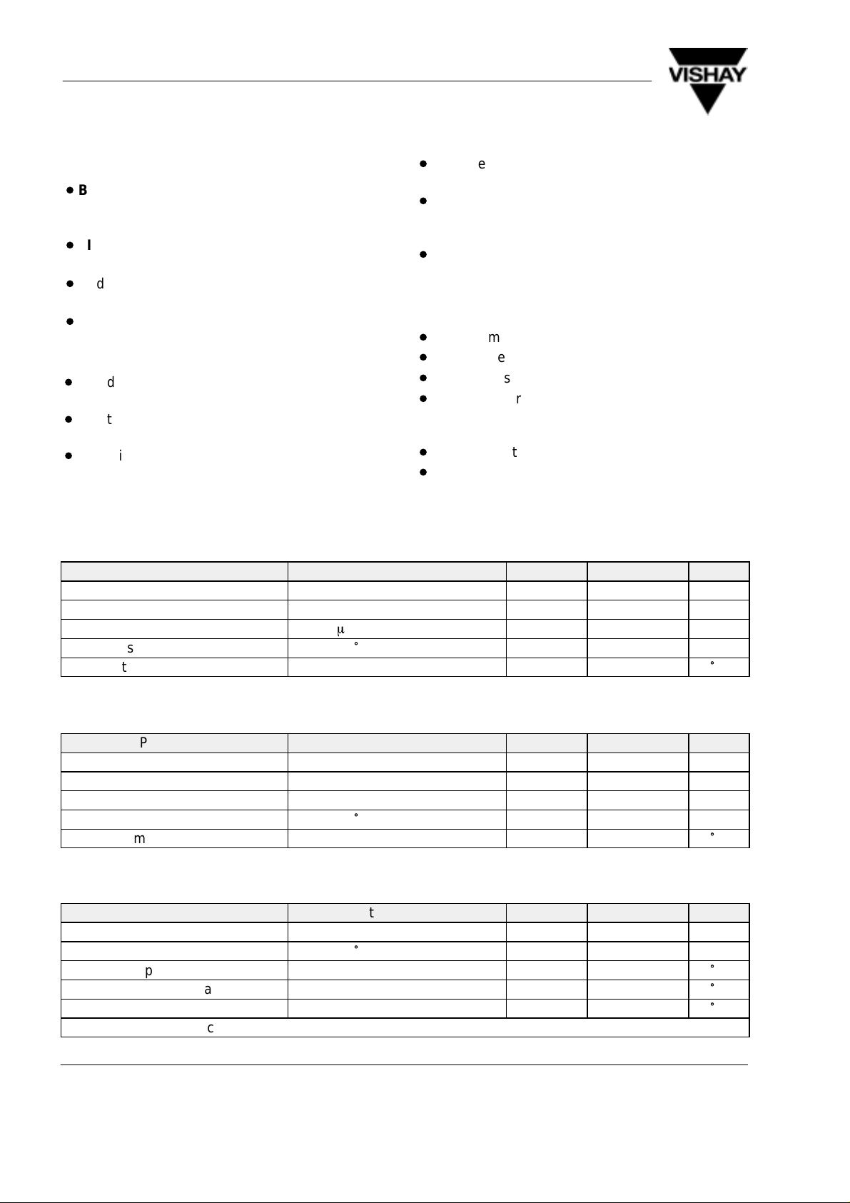
Absolute Maximum Ratings
Input (Emitter)
Parameter T est Conditions Symbol Value Unit
Reverse voltage V
Forward current I
Forward surge current tp ≤ 10 ms I
Power dissipation T
Junction temperature T
≤ 25°C P
amb
R
F
FSM
V
5 V
80 mA
3 A
100 mW
j
100
°
C
Output (Detector)
Parameter T est Conditions Symbol Value Unit
Off state output terminal voltage V
On state RMS current I
Peak surge current, non-repetitive tp ≤ 10 ms I
Power dissipation T
≤ 25°C P
amb
TRMS
TMS
Junction temperature T
Coupler
Parameter T est Conditions Symbol V alue Unit
Isolation test voltage (RMS) VIO
Total power dissipation T
Ambient temperature range T
Storage temperature range T
Soldering temperature 2 mm from case, t ≤ 10 s T
1)
Related to standard climate 23/50 DIN 50014
www.vishay.de • FaxBack +1-408-970-5600
2 (9)
≤ 25°C P
amb
DRM
V
j
tot
amb
stg
sd
400 V
100 mA
1.5 A
300 mW
100
1)
3.75 kV
°
C
350 mW
–40 to +85
–55 to +100
260
Document Number 83505
Rev. A5, 13–Sep–99
°
C
°
C
°
C

K3020P(G) Series
FT FT
ggg
S L
Vishay Telefunken
Electrical Characteristics (T
amb
= 25°C)
Input (Emitter)
Parameter Test Conditions Symbol Min. Typ. Max. Unit
Forward voltage IF = 50 mA V
Junction capacitance VR = 0, f = 1 MHz C
F
j
1.25 1.6 V
50 pF
Output (Detector)
Parameter Test Conditions Symbol Min. Typ. Max. Unit
Forward peak off-state
I
= 100 nA V
DRM
DRM
1)
400 V
voltage (repetitive)
Peak on-state voltage ITM = 100 mA V
TM
Critical rate of rise of IFT = 0, IFT = 30 mA (dv/dt)
off-state voltage
1)
Test voltage must be applied within dv/dt ratings
(dv/dt)
cr
crq
0.1 0.2 V/ms
1.5 3 V
10 V/ms
Coupler
Parameter Test Conditions Type Symbol Min. Typ. Max. Unit
Emitting diode trigger VS = 3 V, RL = 150 WK3020P(G) I
current
K3021P(G) I
K3022P(G) I
K3023P(G) I
Holding current IF = 10 mA, VS ≥ 3 V I
Note: IFT is defined as a minimum trigger current
FT
FT
FT
FT
H
15 30 mA
8 15 mA
5 10 mA
2 5 mA
100
m
A
Document Number 83505
Rev. A5, 13–Sep–99
R
S
V~
I
FT
R
L
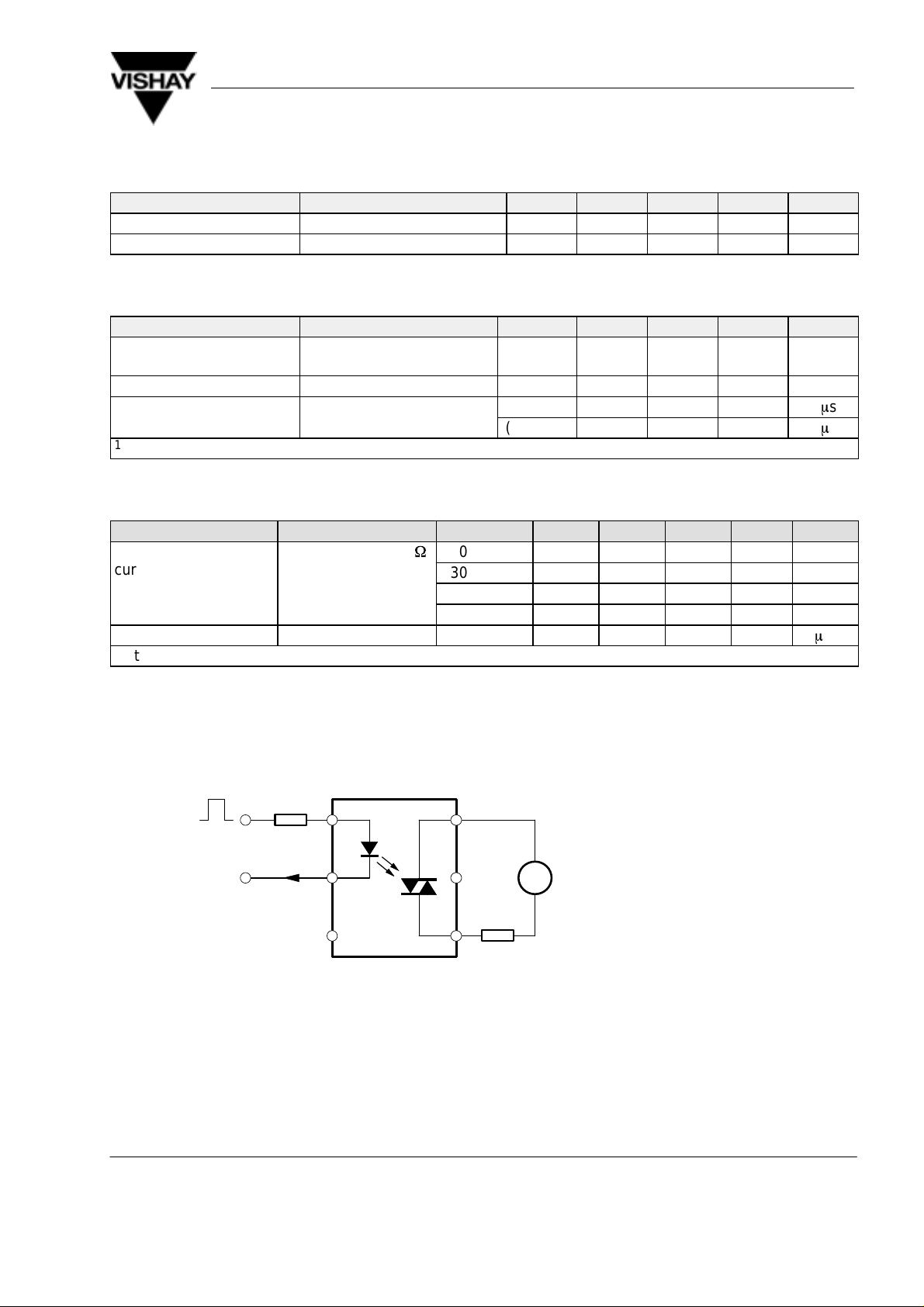
95 10813
Figure 1. Test circuit for dv/dtcr and dv/dt
Test condition:
dv/dt
cr
VS = 2/3 V
(Sine wave)
R
= 33 kΩ
L
dv/dt
V
eff
(Sine wave)
R
= 2 kΩ
L
crp
www.vishay.de • FaxBack +1-408-970-5600
crq
= 30 V
DRM
3 (9)
 Loading...