

Optocoupler with Phototriac Output
Description
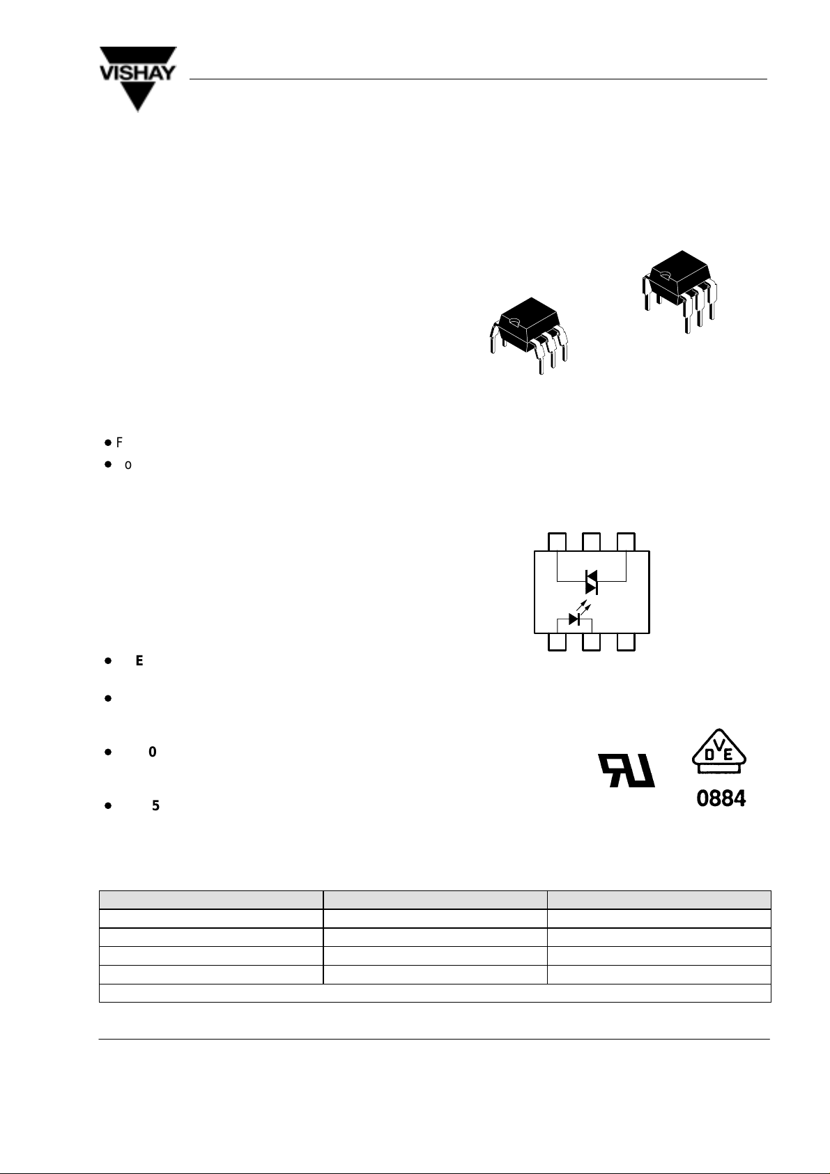
The K3020P(G) series consists of a phototransistor
optically coupled to a gallium arsenide infrared-emitting diode in a 6-lead plastic dual inline package. The
elements are mounted on one leadframe using a
coplanar technique, providing a fixed distance between input and output for highest safety
requirements.
Applications
K3020P(G) Series
Vishay Telefunken
Circuits for safe protective separation against electrical shock according to safety class II (reinforced
isolation):
D
For appl. class I – IV at mains voltage ≤ 300 V
D
For appl. class I – III at mains voltage ≤ 600 V
according to VDE 0884, table 2, suitable for:
Monitors, air conditioners, line switches, solid
state relays, microwaves.
VDE Standards
These couplers perform safety functions according
to the following equipment standards:
D
VDE 0884
Optocoupler for electrical safety requirements
D
IEC 950/EN 60950
Office machines (applied for reinforced isolation
for mains voltage ≤ 400 V
D
VDE 0804
Telecommunication apparatus and data
processing
D
IEC 65 Safety for mains-operated electronic and
related household apparatus
RMS
)
14827
~~
6
54
95 10812
2
3
1
A (+) C (–) nc
Note: Pin 5 must not be connected
Order Instruction
Ordering Code CTR Ranking Remarks
K3020P, K3020PG
K3021P, K3021PG
K3022P, K3022PG
K3023P, K3023PG
1)
G = Leadform 10.16 mm; G is not marked on the body
Document Number 83505
Rev. A5, 13–Sep–99
1)
1)
1)
1)
< 30 mA
< 15 mA
< 10 mA
< 5 mA
www.vishay.de • FaxBack +1-408-970-5600
1 (9)
K3020P(G) Series
Vishay Telefunken
Features
Approvals:
D
BSI: BS EN 41003, BS EN 60095 (BS 415),
BS EN 60950 (BS 7002),
Certificate number 7081 and 7402
D
FIMKO (SETI): EN 60950,
Certificate number 12398
D
Underwriters Laboratory (UL) 1577 recognized,
file number E-76222
D
VDE 0884, Certificate number 94778
VDE 0884 related features:
D
Rated impulse voltage (transient overvoltage)
= 6 kV peak
V
IOTM
D
Isolation test voltage
(partial discharge test voltage) V
D
Rated isolation voltage (RMS includes DC)
V
IOWM
= 600 V
(848 V peak)
RMS
= 1.6 kV
pd
D
Rated recurring peak voltage (repetitive)
= 600 V
V
IORM
D
Creepage current resistance according to
RMS
VDE 0303/IEC 1 12
Comparative Tracking Index: CTI = 275
D
Thickness through insulation ≥ 0.75 mm
General features:
D
Isolation materials according to UL 94-VO
D
Pollution degree 2 (DIN/VDE 0110 resp. IEC 664)
D
Climatic classification 55/100/21 (IEC 68 part 1)
D
Special construction:
Therefore, extra low coupling capacity of
typical 0.2 pF, high Common Mode Rejection
offered into 4 groups
D
I
FT
D
Coupling System C
Absolute Maximum Ratings
Input (Emitter)
Parameter T est Conditions Symbol Value Unit
Reverse voltage V
Forward current I
Forward surge current tp ≤ 10 ms I
Power dissipation T
Junction temperature T
≤ 25°C P
amb
R
F
FSM
V
5 V
80 mA
3 A
100 mW
j
100
°
C
Output (Detector)
Parameter T est Conditions Symbol Value Unit
Off state output terminal voltage V
On state RMS current I
Peak surge current, non-repetitive tp ≤ 10 ms I
Power dissipation T
≤ 25°C P
amb
TRMS
TMS
Junction temperature T
Coupler
Parameter T est Conditions Symbol V alue Unit
Isolation test voltage (RMS) VIO
Total power dissipation T
Ambient temperature range T
Storage temperature range T
Soldering temperature 2 mm from case, t ≤ 10 s T
1)
Related to standard climate 23/50 DIN 50014
www.vishay.de • FaxBack +1-408-970-5600
2 (9)
≤ 25°C P
amb
DRM
V
j
tot
amb
stg
sd
400 V
100 mA
1.5 A
300 mW
100
1)
3.75 kV
°
C
350 mW
–40 to +85
–55 to +100
260
Document Number 83505
Rev. A5, 13–Sep–99
°
C
°
C
°
C
K3020P(G) Series
FT FT
ggg
S L
Vishay Telefunken
Electrical Characteristics (T
amb
= 25°C)
Input (Emitter)
Parameter Test Conditions Symbol Min. Typ. Max. Unit
Forward voltage IF = 50 mA V
Junction capacitance VR = 0, f = 1 MHz C
F
j
1.25 1.6 V
50 pF
Output (Detector)
Parameter Test Conditions Symbol Min. Typ. Max. Unit
Forward peak off-state
I
= 100 nA V
DRM
DRM
1)
400 V
voltage (repetitive)
Peak on-state voltage ITM = 100 mA V
TM
Critical rate of rise of IFT = 0, IFT = 30 mA (dv/dt)
off-state voltage
1)
Test voltage must be applied within dv/dt ratings
(dv/dt)
cr
crq
0.1 0.2 V/ms
1.5 3 V
10 V/ms
Coupler
Parameter Test Conditions Type Symbol Min. Typ. Max. Unit
Emitting diode trigger VS = 3 V, RL = 150 WK3020P(G) I
current
K3021P(G) I
K3022P(G) I
K3023P(G) I
Holding current IF = 10 mA, VS ≥ 3 V I
Note: IFT is defined as a minimum trigger current
FT
FT
FT
FT
H
15 30 mA
8 15 mA
5 10 mA
2 5 mA
100
m
A
Document Number 83505
Rev. A5, 13–Sep–99
R
S
V~
I
FT
R
L
95 10813
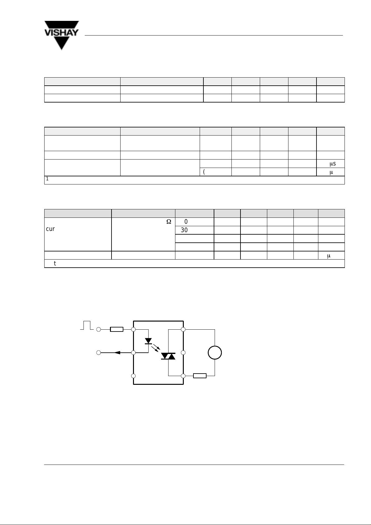
Figure 1. Test circuit for dv/dtcr and dv/dt
Test condition:
dv/dt
cr
VS = 2/3 V
(Sine wave)
R
= 33 kΩ
L
dv/dt
V
eff
(Sine wave)
R
= 2 kΩ
L
crp
www.vishay.de • FaxBack +1-408-970-5600
crq
= 30 V
DRM
3 (9)

K3020P(G) Series
Vishay Telefunken
IF y I
FT
IF = 0
dv / dt
crq
dv/dtcrHighest value of the “rate of rise of off-state voltage” which does not cause any switching from the
dv/dt
off-state to the on-state
Highest value of the “rate of rise of communicating voltage” which does not switch on the device again,
crq
after the voltage has decreased to zero and the trigger current is switched from IFT to zero
Figure 2.
dv / dt
95 10814
cr
+5 V
TTL
270 Ω
Galvanical separation
Figure 3. Motor control circuit
0.1 µF
M
VAC ~
95 10815
www.vishay.de • FaxBack +1-408-970-5600
4 (9)
Document Number 83505
Rev. A5, 13–Sep–99

K3020P(G) Series
gg
Tr test
Vishay Telefunken
Maximum Safety Ratings (according to VDE 0884) see figure 4
This device is used for protective separation against electrical shock only within the maximum safety ratings.
This must be ensured by using protective circuits in the applications.
Input (Emitter)
Parameters Test Conditions Symbol Value Unit
Forward current I
Output (Detector)
Parameters Test Conditions Symbol Value Unit
Power dissipation T
≤ 25°C P
amb
Coupler
Parameters Test Conditions Symbol V alue Unit
Rated impulse voltage V
Safety temperature T
si
si
IOTM
si
130 mA
600 mW
6 kV
150
°
C
Insulation Rated Parameters (according to VDE 0884)
Parameter Test Conditions Symbol Min. Typ. Max. Unit
Partial discharge test voltage –
Routine test
Partial discharge test voltage – tTr = 60 s, t
Lot test (sample test)
Insulation resistance VIO = 500 V R
Insulation resistance VIO = 500 V,
Insulation resistance VIO = 500 V,
675
600
525
450
375
300
225
150
Isi (mA)
75
0
0 25 50 75 100 125 150
Psi (mW)
T
amb
( °C )95 10925
100%, t
= 1 s V
test
= 10 s, V
test
(see figure 5)
= 100°C
T
amb
= 150°C
T
amb
(construction test only)
V
V
IOWM
V
13930
IOTM
V
Pd
IORM
pd
IOTM
V
pd
IO
R
IO
R
IO
0
t
1
1.6 kV
6 kV
1.3 kV
12
10
11
10
9
10
t1, t2 = 1 to 10 s
t
, t4 = 1 s
3
t
= 10 s
test
t
= 12 s
stres
t
t3t
test
tTr = 60 s
t
t
stres
2
W
W
W
4
t
Figure 4. Derating diagram
Document Number 83505
Rev. A5, 13–Sep–99
Figure 5. Test pulse diagram for sample test according to
DIN VDE 0884
www.vishay.de • FaxBack +1-408-970-5600
5 (9)

K3020P(G) Series
Vishay Telefunken
Typical Characteristics (T
400
Coupled device
300
Phototransistor
200
IR-diode
100
tot
P – Total Power Dissipation ( mW )
0
0 20406080100
T
– Ambient Temperature ( °C )96 11701
amb
Figure 6. Total Power Dissipation vs.
Ambient Temperature
1000.0
100.0
= 25_C, unless otherwise specified)
amb
1.5
1.4
1.3
1.2
1.1
1.0
0.9
0.8
0.7
TMrel
0.6
V – Relative On–State Voltage
0.5
–30 –20 –10 0 10 20 30 40 50 60 70 80
T
– Ambient Temperature ( °C )96 11923
amb
Figure 9. Relative On - State vs. Ambient Temperature
100
VDR=100V
I
=0
F
IFw
I
FT
IT=100mA
10.0
1.0
F
I – Forward Current ( mA )
0.1
0 0.2 0.4 0.6 0.8 1.0 1.2 1.4 1.6 1.8 2.0
VF – Forward Voltage ( V )96 11862
Figure 7. Forward Current vs. Forward Voltage
1.5
1.4
1.3
1.2
1.1
1.0
0.9
0.8
0.7
0.6
FTrel
0.5
I – Relative Threshold Forward Current
–30 –20–10 0 10 20 30 40 50 60 70 80
T
– Ambient Temperature ( °C )96 11922
amb
VS=3V
R
=150
L
W
10
DRM
I – Off–State Current ( nA )
1
20 30 40 50 60 70 80 90 100
T
– Ambient Temperature ( °C )96 11924
amb
Figure 10. Off - State Current vs. Ambient Temperature
250
200
150
100
50
0
–50
–100
–150
TM
I – On–State Current ( mA )
–200
–250
–2.5–2.0–1.5–1.0–0.5 0.0 0.5 1.0 1.5 2.0 2.5
VTM – On–State Voltage ( V )96 11926
IFT=30mA
Figure 8. Relative Threshold Forward Current vs.
Ambient Temperature
www.vishay.de • FaxBack +1-408-970-5600
6 (9)
Figure 11. On - State Current vs. Ambient Temperature
Document Number 83505
Rev. A5, 13–Sep–99

K3020P(G) Series
Vishay Telefunken
250
200
150
100
50
0
–50
–100
–150
TM
I – On–State Current ( mA )
–200
–250
–2.5–2.0–1.5–1.0–0.5 0.0 0.5 1.0 1.5 2.0 2.5
VTM – On–State Voltage ( V )96 11925
IFT=15mA
Figure 12. On - State Current vs. Ambient Temperature
Dimensions of K302.PG in mm
Date
Code
(YM)
Type
XXXXXX
918 A TK 63
V
DE
Coupling
System
Indicator
Figure 13. Marking example
0884
15090
Company
Logo
Production
Location
Safety
Logo
Document Number 83505
Rev. A5, 13–Sep–99
14771
www.vishay.de • FaxBack +1-408-970-5600
7 (9)

K3020P(G) Series
Vishay Telefunken
Dimensions of K302.P in mm
www.vishay.de • FaxBack +1-408-970-5600
8 (9)
14770
Document Number 83505
Rev. A5, 13–Sep–99

K3020P(G) Series
Vishay Telefunken
Ozone Depleting Substances Policy Statement
It is the policy of Vishay Semiconductor GmbH to
1. Meet all present and future national and international statutory requirements.
2. Regularly and continuously improve the performance of our products, processes, distribution and operating
systems with respect to their impact on the health and safety of our employees and the public, as well as
their impact on the environment.
It is particular concern to control or eliminate releases of those substances into the atmosphere which are known as
ozone depleting substances (ODSs).
The Montreal Protocol (1987) and its London Amendments (1990) intend to severely restrict the use of ODSs and
forbid their use within the next ten years. V arious national and international initiatives are pressing for an earlier ban
on these substances.
Vishay Semiconductor GmbH has been able to use its policy of continuous improvements to eliminate the use of
ODSs listed in the following documents.
1. Annex A, B and list of transitional substances of the Montreal Protocol and the London Amendments respectively
2.Class I and II ozone depleting substances in the Clean Air Act Amendments of 1990 by the Environmental
Protection Agency (EPA) in the USA
3. Council Decision 88/540/EEC and 91/690/EEC Annex A, B and C (transitional substances) respectively.
Vishay Semiconductor GmbH can certify that our semiconductors are not manufactured with ozone depleting
substances and do not contain such substances.
We reserve the right to make changes to improve technical design and may do so without further notice.
Parameters can vary in different applications. All operating parameters must be validated for each customer application
by the customer. Should the buyer use Vishay Telefunken products for any unintended or unauthorized application, the
buyer shall indemnify Vishay Telefunken against all claims, costs, damages, and expenses, arising out of, directly or
indirectly , any claim of personal damage, injury or death associated with such unintended or unauthorized use.
Document Number 83505
Rev. A5, 13–Sep–99
Vishay Semiconductor GmbH, P.O.B. 3535, D-74025 Heilbronn, Germany
Telephone: 49 (0)7131 67 2831, Fax number: 49 (0)7131 67 2423
www.vishay.de • FaxBack +1-408-970-5600
9 (9)
 Loading...