

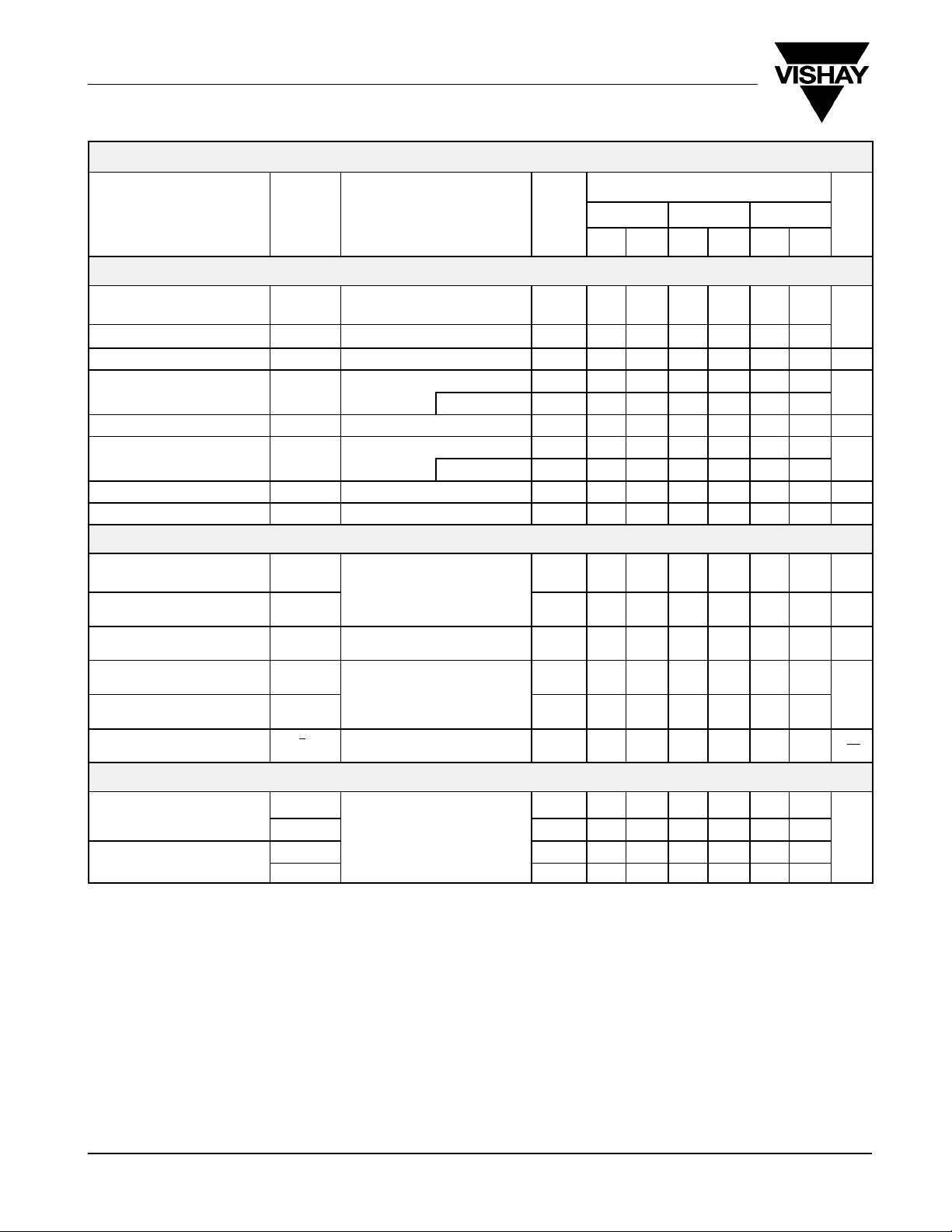
PRODUCT SUMMARY
J/SST111 Series
Vishay Siliconix
N-Channel JFETs
J111 SST111
J112 SST112
J113 SST113
Part Number V
J/SST111
J/SST112 –1 to –5 50 5 4
J/SST113 v–3 100 5 4
(V)
r
GS(off)
–3 to –10 30 5 4
DS(on)
Max (W)
I
Typ (pA) tON Typ (ns)
D(off)
FEATURES BENEFITS APPLICATIONS
D Low On-Resistance: 111 < 30 W
D Fast Switching—tON: 4 ns
D Low Leakage: 5 pA
D Low Capacitance: 3 pF
D Low Insertion Loss
D Low Error Voltage
D High-Speed Analog Circuit Performance
D Negligible “Off-Error,” Excellent Accuracy
D Good Frequency Response, Low Glitches
D Eliminates Additional Buffering
D Analog Switches
D Choppers
D Sample-and-Hold
D Normally “On” Switches
D Current Limiters
DESCRIPTION
The J/SST111 series consists of all-purpose analog switches
designed to support a wide range of applications. The
J/SST113 are useful in a high-gain amplifier mode.
The J series, TO-226AA (TO-92) plastic package, provides
low cost, while the SST series, TO236 (SOT-23) package,
provides surface-mount capability. Both the J and SST series
are available in tape-and-reel for automated assembly (see
Packaging Information).
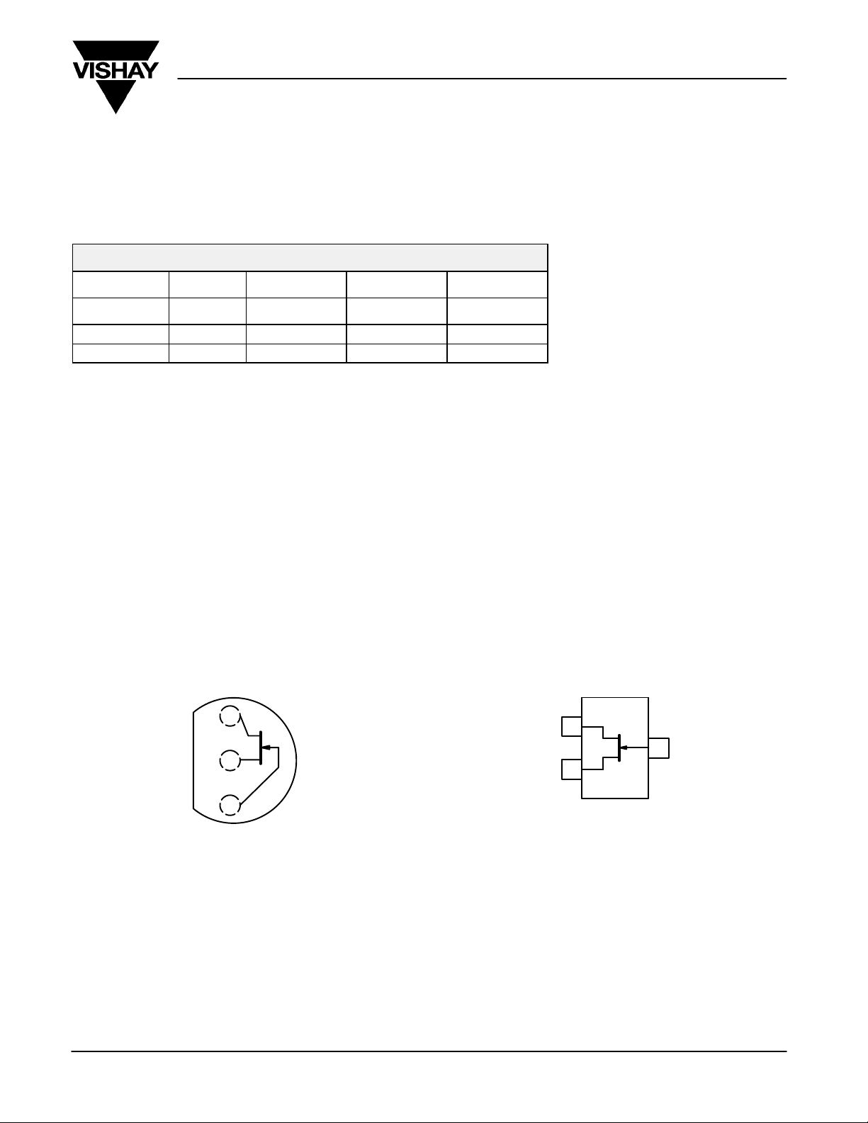
TO-226AA (TO-92)
For similar products in TO-206AA(TO-18) packaging, see the
2N/PN/SST4391 series, 2N4856A/4857A/4858A, and
2N5564/5565/5566 (duals) data sheets.
TO-236 (SOT-23)
D
S
G
1
2
3
Top View
J111
J112
J113
ABSOLUTE MAXIMUM RATINGS
Gate-Drain, Gate-Source Voltage –35 V. . . . . . . . . . . . . . . . . . . . . . . . . . . . . . .
Gate Current 50 mA. . . . . . . . . . . . . . . . . . . . . . . . . . . . . . . . . . . . . . . . . . . . . . . . .
Lead Temperature (
Storage Temperature –55 to 150_C. . . . . . . . . . . . . . . . . . . . . . . . . . . . . . . . . . .
Operating Junction Temperature –55 to 150_C. . . . . . . . . . . . . . . . . . . . . . . . . .
For applications information see AN105.
Document Number: 70232
S-04028—Rev. E, 04-Jun-01
1
/16” from case for 10 seconds) 300 _C. . . . . . . . . . . . . .
D
1
G
3
S
2
Top View
SST111 (C1)*
SST112 (C2)*
SST113 (C3)*
*Marking Code for TO-236
Power Dissipation
(TO-236) 350 mW. . . . . . . . . . . . . . . . . . . . . . . . . . . . . . . . . . . . . . . . . . . . . . . . . .
(TO-226AA) 360 mW. . . . . . . . . . . . . . . . . . . . . . . . . . . . . . . . . . . . . . . . . . . . . . .
Notes
a. Derate 2.8 mW/_C above 25_C
a
www.vishay.com
7-1
J/SST111 Series
-10
Vishay Siliconix
SPECIFICATIONS (TA = 25_C UNLESS OTHERWISE NOTED)
Parameter Symbol Test Conditions TypaMin Max Min Max Min Max Unit
Static
J/SST111
Limits
J/SST112 J/SST113
Gate-Source
Breakdown Voltage
Gate-Source Cutoff Voltage V
Saturation Drain Current
Gate Reverse Current I
Gate Operating Current I
Drain Cutoff Current I
Drain-Source On-Resistance r
Gate-Source Forward Voltage V
b
V
(BR)GSS
Dynamic
Common-Source Forward
Transconductance
Common-Source
Output Conductance
Drain-Source On-Resistance r
Common-Source
Input Capacitance
Common-Source Reverse Transfer
Capacitance
Equivalent Input
Noise Voltage
GS(off)
I
DSS
GSS
G
D(off)
DS(on)
GS(F)
g
fs
g
os
ds(on)
C
iss
C
rss
e
n
IG = –1 mA , VDS = 0 V
VDS = 5 V, ID = 1 mA –3
VDS = 15 V, VGS = 0 V 20 5 2 mA
VGS = –15 V, VDS = 0 V –0.005 –1 –1 –1
TA = 125_C
VDG = 15 V, ID = 10 mA –5 pA
VDS = 5 V, VGS = –10 V 0.005 1 1 1
TA = 125_C
VGS = 0 V, VDS = 0.1 V 30 50 100
IG = 1 mA , VDS = 0 V 0.7 V
VDS = 20 V, ID = 1 mA
VDS = 20 V, ID = 1 mA
f = 1 kHz
VGS = 0 V, ID = 0 mA
f = 1 kHz
VDS = 0 V, VGS = -10 V
VDS = 0 V, VGS =
f = 1 MHz
VDG = 10 V, ID = 1 mA
f = 1 kHz
V
–55
–35 –35 –35
–10 –1 –5 –3
–3
3
6 mS
25
30 50 100
7 12 12 12
3 5 5 5
3
V
V
nA
nA
W
mS
W
pF
nV⁄
√Hz
Switching
t
Turn-On Time
Turn-Off Time
Notes
a. Typical values are for DESIGN AID ONLY, not guaranteed nor subject to production testing. NCB
b. Pulse test: PW v300 ms duty cycle v3%.
www.vishay.com
7-2
d(on)
t
d(off)
t
r
t
f
VDD = 10 V, V
VDD = 10 V, V
See Switching Circuit
GS(H)
GS(H)
= 0 V
= 0 V
2
2
6
15
Document Number: 70232
S-04028—Rev. E, 04-Jun-01
ns

TYPICAL CHARACTERISTICS (TA = 25_C UNLESS OTHERWISE NOTED)
On-Resistance and Drain Current
100
vs. Gate-Source Cutoff Voltage
200
r
@ ID = 1 mA, VGS = 0
DS
I
@ VDS = 20 V, VGS = 0
DSS
80
I
DSS
– Saturation Drain Current (mA)
160
100
80
On-Resistance vs. Drain Current
TA = 25° C
J/SST111 Series
Vishay Siliconix
I
r
60
DS
DSS
40
– Drain-Source On-Resistance ( Ω )
20
DS(on)
r
0
0 –10
–2 –4 –6 –8
V
– Gate-Source Cutoff Voltage (V)
GS(off)
On-Resistance vs. Temperature
200
ID = 1 mA
changes X 0.7%/_C
r
DS
160
120
80
40
– Drain-Source On-Resistance ( Ω )
DS(on)
r
0
–35
–55 25 125
5 45 65 105 –2 –4 –6 –8
–15 85
T
– Temperature ( _C)
A
V
GS(off)
= –2 V
–4 V
–8 V
120
80
40
0
– Drain-Source On-Resistance ( Ω )
DS(on)
r
Switching Time (ns)
V
= –2 V
GS(off)
60
40
20
–4 V
–8 V
0
1 10 100
– Drain Current (mA)
I
D
5
4
Turn-On Switching
tr approximately independent of I
VDD = 5 V, RG = 50 Ω
V
= –10 V
GS(L)
t
r
D
3
t
@
d(on)
I
= 12 mA
D
2
t
d(on)
I
= 3 mA
D
@
1
0
0 –10
– Gate-Source Cutoff Voltage (V)
V
GS(off)
30
t
independent of device V
d(off)
V
= 5 V, V
DD
24
18
12
t
Switching Time (ns)
d(off)
6
V
0
010
2468 –4 –8 –12 –16
Document Number: 70232
S-04028—Rev. E, 04-Jun-01
Turn-Off Switching
= –10 V
GS(L)
tf @
= –8 V
GS(off)
I
– Drain Current (mA)
D
GS(off
V
)
GS(off)
tf @
= –2 V
30
24
18
12
Capacitance (pF)
6
0
0
Capacitance vs. Gate-Source Voltage
f = 1 MHz
C
@ VDS = 0 V
iss
C
@ VDS = 0 V
rss
V
– Gate-Source Voltage (V)
GS
www.vishay.com
–20
7-3

J/SST111 Series
Vishay Siliconix
TYPICAL CHARACTERISTICS (TA = 25_C UNLESS OTHERWISE NOTED)
100
Noise Voltage vs. Frequency
VDS = 10 V
10
ID = 1 mA
n – Noise Voltage nV / Hz
e
ID = 10 mA
1
10 100 1 k 100 k10 k
10 nA
1 nA
Gate Leakage Current
TA = 125_C
ID = 10 mA
100 pA
10 pA
– Gate Leakage
G
I
TA = 25_C
10 mA
1 pA
1 mA
I
GSS
@ 125_C
1 mA
I
@ 25_C
GSS
Forward Transconductance and Output Conductance
vs. Gate-Source Cutoff Voltage
50
gfs and gos @ V
V
= 0 V, f = 1 kHz
GS
= 20 V
DS
40
g
30
fs
g
os
20
10
– Forward Transconductance (mS)
fs
g
0
0
–2 –10
V
GS(off)
–4 –6 –8
– Gate-Source Cutoff Voltage (V)f – Frequency (Hz)
Common-Gate Input Admittance
100
VDG = 10 V
I
= 10 mA
D
= 25_C
T
(mS)
A
10
b
ig
1
g
ig
500
g
os
– Output Conductance
250
(mS)
0
0.1 pA
030
100
10
(mS)
1
0.1
100 1000200 500
www.vishay.com
7-4
6 121824
VDG – Drain-Gate Voltage (V)
100 1000200 500
f – Frequency (MHz)
Common-Gate Forward Admittance Common-Gate Reverse Admittance
0.1
VDG = 10 V
I
= 10 mA
D
= 25_C
T
A
–g
fg
f – Frequency (MHz)
b
fg
g
fg
10
VDG = 10 V
I
= 10 mA
D
= 25_C
T
A
–b
1.0
rg
(mS)
–g
0.1
rg
0.01
100 1000200 500
f – Frequency (MHz)
+g
rg
Document Number: 70232
S-04028—Rev. E, 04-Jun-01

TYPICAL CHARACTERISTICS (TA = 25_C UNLESS OTHERWISE NOTED)
J/SST111 Series
Vishay Siliconix
100
Common-Gate Output Admittance
VDG = 10 V
I
= 10 mA
D
= 25_C
T
A
b
10
(mS)
1
0.1
100 1000200 500
f – Frequency (MHz)
40
V
Output Characteristics
= –4 V
GS(off)
32
24
16
– Drain Current (mA)
D
I
8
0
0 1.0
0.2 0.4 0.6 0.8
V
– Drain-Source Voltage (V)
DS
og
g
og
VGS = 0 V
–0.5
–1.0
–1.5
–2.0
–2.5
–3.0
100
V
GS(off)
80
60
40
– Drain Current (mA)I
D
I
20
0
010
100
V
GS(off)
80
60
25_C
40
– Drain Current (mA)
D
20
0
0 –5
Output Characteristics
= –4 V
VGS = 0 V
–0.5
–1.0
–1.5
–2.0
–2.5
2468
V
– Drain-Source Voltage (V)
DS
Transfer Characteristics
= –4 V
TA = –55_C
125_C
–1 –2 –3 –4
V
– Gate-Source Voltage (V)
GS
VDS = 20 V
SWITCHING TIME TEST CIRCUIT
J/SST111 J/SST112 J/SST113
V
GS(L)
RL*
I
D(on)
*Non-inductive
–12 V –7 V –5 V
800 W 1600 W 3200 W
12 mA 6 mA 3 mA
INPUT PULSE SAMPLING SCOPE
Rise Time < 1 ns
Fall Time < 1 ns
Pulse Width 100 ns
PRF 1 MHz
Document Number: 70232
S-04028—Rev. E, 04-Jun-01
Rise Time 0.4 ns
Input Resistance 10 MW
Input Capacitance 1.5 pF
V
V
GS(H)
GS(L)
V
GS
Scope
1 kW
51 W
51 W
V
DD
R
L
OUT
www.vishay.com
7-5

 Loading...