

PRODUCT SUMMARY
J/SST108 Series
Vishay Siliconix
N–Channel JFETs
J108 SST108
J109 SST109
J110 SST110
Part Number V
J/SST108
J/SST109
J/SST110
(V)
r
GS(off)
–3 to –10 8 20 4
–2 to –6 12 20 4
–0.5 to –4 18 20 4
DS(on)
Max (W)
I
Typ (pA) tON Typ (ns)
D(off)
FEATURES BENEFITS APPLICATIONS
D Low On-Resistance: J108 <8 W
D Fast Switching—tON: 4 ns
D Low Leakage: 20 pA
D Low Capacitance: 11 pF
D Low Insertion Loss
D Low Error Voltage
D High-Speed Analog Circuit Performance
D Negligible “Off-Error” Excellent Accuracy
D Good Frequency Response
D Eliminates Additional Buffering
D Analog Switches
D Choppers
D Sample-and-Hold
D Normally “On” Switches
D Current Limiters
DESCRIPTION
The J/SST108 series is designed with high-performance
analog switching applications in mind. It features low
on-resistance, good off-isolation, and fast switching.
The SST108 series is comprised of surface-mount
devices featuring the lowest r
of any TO-236
DS(on)
(SOT-23) JFET device.
The TO-226AA (TO-92) plastic package provides a
low-cost option. Both the J and SST series are available
in tape-and-reel for automated assembly (see Packaging
Information). For similar products packaged in
TO-206AC (TO-52), see the 2N5432/5433/5434 data
sheet.
Document Number: 70231
S-04028—Rev. E, 04-Jun-01
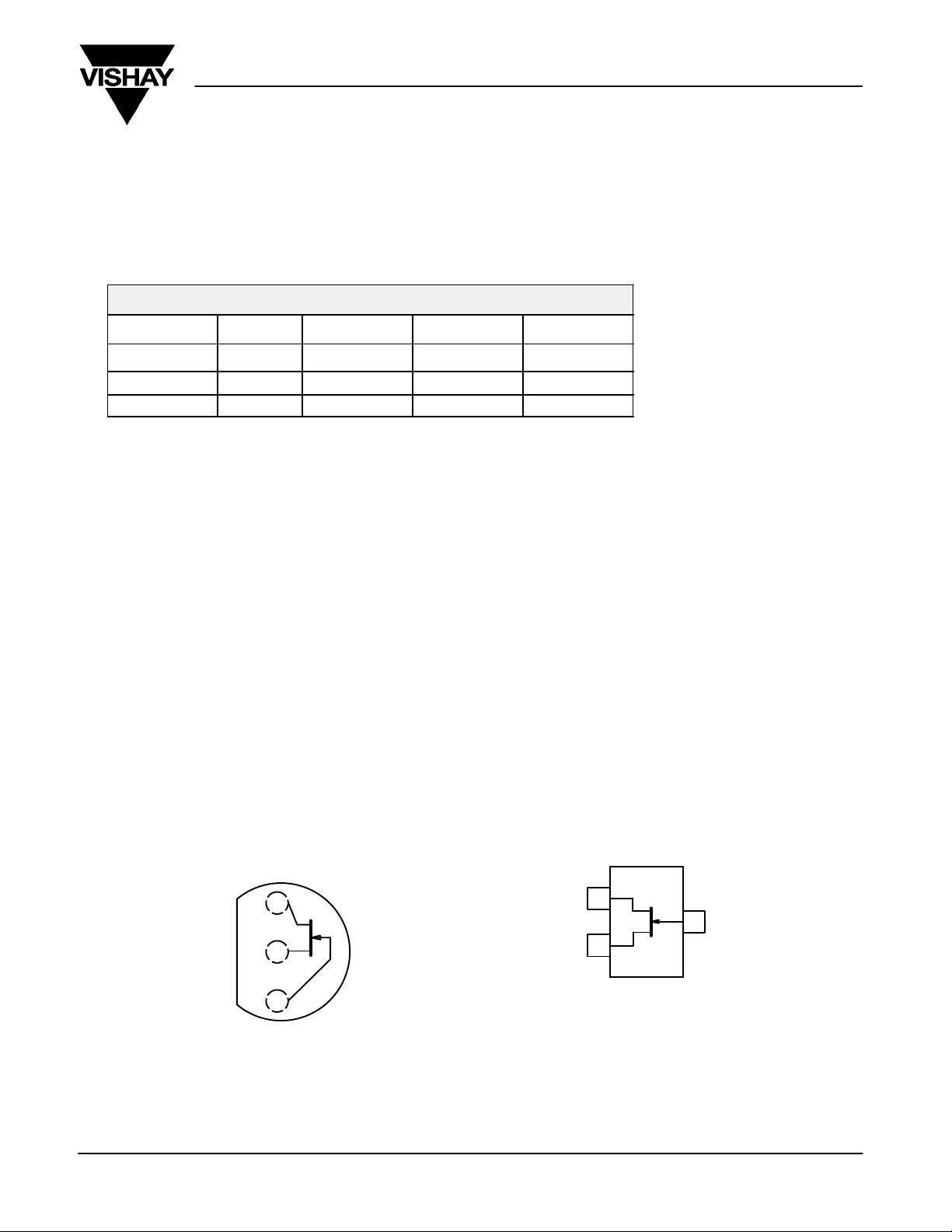
TO-226AA
(TO-92)
D
S
G
Top View
J108, J109, J110
TO-236
(SOT-23)
1
1
2
3
D
S
2
Top View
SST108 (I8)*
SST109 (I9)*
SST110 (I0)*
*Marking Code for TO-236
3
G
www.vishay.com
7-1
J/SST108 Series
Vishay Siliconix
ABSOLUTE MAXIMUM RATINGS
Gate-Drain, Gate-Source Voltage –25 V. . . . . . . . . . . . . . . . . . . . . . . . . . . . . . .
Gate Current 50 mA. . . . . . . . . . . . . . . . . . . . . . . . . . . . . . . . . . . . . . . . . . . . . . . . .
Lead Temperature (1/16” from case for 10 sec.) 300_C. . . . . . . . . . . . . . . . . . .
Storage Temperature –55 to 150_C. . . . . . . . . . . . . . . . . . . . . . . . . . . . . . . . . . .
SPECIFICATIONS (TA = 25_C UNLESS OTHERWISE NOTED)
Parameter Symbol Test Conditions TypaMin Max Min Max Min Max Unit
Static
Gate-Source
Breakdown Voltage
Gate-Source Cutoff Voltage V
Saturation Drain Current
Gate Reverse Current I
Gate Operating Current I
Drain Cutoff Current I
Drain-Source
On-Resistance
Gate-Source
Forward Voltage
b
Dynamic
Common-Source
Forward Transconductance
Common-Source
Output Conductance
Drain-Source
On-Resistance
Common-Source
Common-Source
Input Capacitance
Common-Source Reverse
Common-Source Reverse
Transfer Capacitance
Equivalent Input
Noise Voltage
Switching
Turn-On Time
Turn-Off Time
Notes
a. Typical values are for DESIGN AID ONLY, not guaranteed nor subject to production testing. NIP
b. Pulse test: PW v300 ms duty cycle v3%.
V
(BR)GSS
GS(off)
I
DSS
GSS
D(off)
r
DS(on)
V
GS(F)
g
g
r
ds(on)
C
C
e
t
d(on)
t
d(off)
IG = –1 mA , VDS = 0 V
VDS = 5 V, ID = 1 mA
VDS = 15 V, VGS = 0 V 80 40 10 mA
VGS = –15 V, VDS = 0 V –0.01 –3 –3 –3
G
fs
os
iss
rss
n
t
r
t
f
VDG = 10 V, ID = 10 mA
VDS = 5 V, VGS = –10 V 0.02
VGS = 0 V, VDS v 0.1 V
IG = 1 mA , VDS = 0 V 0.7 V
VDS = 5 V, ID = 10 mA, f = 1 kHz
VGS = 0 V, ID = 0 mA , f = 1 kHz
VDS = 0 V SST 60
VGS = 0 V
f = 1 MHz
VDS = 0 V SST 11
VGS = –10 V
f = 1 MHz
VDG = 5 V, ID = 10 mA
f = 1 kHz
VDD = 1.5 V, V
VDD = 1.5 V, V
See Switching Diagram
GS(H)
GS(H)
Operating Junction Temperature –55 to 150_C. . . . . . . . . . . . . . . . . . . . . . . . .
Power Dissipation
Notes
a. Derate 2.8 mW/_C above 25_C
a
Limits
J/SST108 J/SST109 J/SST110
–32
TA = 125_C
–0.01
TA = 125_C
J Series 60 85 85 85
J Series 11
= 0 V
= 0 V
–25 –25 –25
–3 –10 –2 –6 –0.5 –4
–5
3 3 3
1.0
8
17
0.6
8 12 18
15 15 15
3.5
3
1
4
18
12
350 mW. . . . . . . . . . . . . . . . . . . . . . . . . . . . . . . . . . . . . . . . .
V
V
nA
W
18
mS
W
pF
nV⁄
√Hz
ns
www.vishay.com
7-2
Document Number: 70231
S-04028—Rev. E, 04-Jun-01

TYPICAL CHARACTERISTICS (TA = 25_C UNLESS OTHERWISE NOTED)
On-Resistance and Drain Current
20
16
12
8
vs. Gate-Source Cutoff Voltage
r
@ ID = 10 mA, VGS = 0 V
DS
I
@ VDS = 15 V, VGS = 0 V
DSS
r
DS
I
DSS
1000
I
DSS
– Saturation Drain Current (mA)
800
600
400
50
40
30
20
On-Resistance vs. Drain Current
TA = 25_C
J/SST108 Series
Vishay Siliconix
V
= –2 V
GS(off)
– Drain-Source On-Resistance ( Ω )r
4
DS(on)
r
0
0 –8 –10–4
40
–2 –6
V
– Gate-Source Cutoff Voltage (V) I
GS(off)
On-Resistance vs. Temperature Output Characteristics
ID = 10 mA
changes X 0.7%/_C
r
DS
32
V
GS(off)
24
16
8
– Drain-Source On-Resistance ( Ω )
DS(on)
0
–55 25 125
–15 85
–35 5 45 65 105
– Temperature (_C)
T
A
= –2 V
–4 V
–8 V
200
0
– Drain-Source On-Resistance ( Ω )
10
DS(on)
r
0
1 10 100
100
80
60
40
– Drain Current (mA)
D
I
20
0
06810
– Drain Current (mA)
D
V
= –2 V
GS(off)
24
– Drain-Source Voltage (V)
V
DS
–4 V
–8 V
VGS= 0 V
–0.2 V
–0.4 V
–0.6 V
–0.8 V
5
tr approximately independent of I
V
= 1.5 V, R
DD
V
4
GS(L)
3
t
@ ID = 10 mA
d(on)
2
Switchng Time (ns)
1
t
r
0
0 –6 –8 –10
–2 –4
– Gate-Source Cutoff Voltage (V) ID – Drain Current (mA)
V
GS(off)
Document Number: 70231
S-04028—Rev. E, 04-Jun-01
Turn-On Switching Turn-Off Switching
D
= –10 V
= 50 Ω
G
t
d(on)
@ ID = 25 mA
30
t
independent
d(off)
of device V
V
24
t
f
18
V
= –8 V
12
GS(off)
= 1.5 V, V
DD
V
GS(off)
GS(off)
GS(L)
= –2 V
Switching Time (ns)
t
6
d(off)
0
0152010525
= –10 V
www.vishay.com
7-3

J/SST108 Series
Vishay Siliconix
TYPICAL CHARACTERISTICS (TA = 25_C UNLESS OTHERWISE NOTED)
100
Capacitance vs. Gate-Source Voltage Transconductance vs. Drain Current
VDS = 0 V
f = 1 MHz
80
60
40
Capacitance (pF)
20
C
iss
C
rss
0
0 –12 –16–8–4 –20
VGS – Gate-Source Voltage (V) ID – Drain Current (mA)
Forward Transconductance and Output Conductance
vs. Gate-Source Cutoff Voltage
200
gfs and gos @ VDS = 5 V
V
= 0 V, f = 1 kHz
160
120
GS
g
fs
80
g
os
100
V
= –4 V
GS(off)
TA = –55_C
10
– Forward Transconductance (mS)
fs
g
125_C
25_C
VDS = 5 V
f = 1 kHz
1
1 10 100
50
100
Noise Voltage vs. Frequency
VDS = 5 V
g
os
40
– Output Conductance (µS)
30
10
20
ID = 10 mA
40
– Forward Transconductance (mS)
fs
g
0
0
100 nA
TA = 125_C
10 nA
1 nA
100 pA
– Gate Leakage
G
I
TA = 25_C
10 pA
1 pA
04812
–2 –6
– Gate-Source Cutoff Voltage (V)
GS(off)
Gate Leakage Current
ID =10 mA5 mA
1 mA
I
@ 125_C
GSS
10 mA
V
– Drain-Gate Voltage (V)
DG
1 mA
I
GSS
–8 –10–4
5 mA
@ 25_C
16 20
10
0
n – Noise Voltage nV / Hz
e
40 mA
1
10 100 1 k 100 k10 k
f – Frequency (Hz)V
Common Gate Input Admittance
100
g
ig
10
(mS)
1
0.1
10 10050
b
ig
20
f – Frequency (MHz)
TA = 25_C
V
= 20 V
DG
I
= 20 mA
D
www.vishay.com
7-4
Document Number: 70231
S-04028—Rev. E, 04-Jun-01

TYPICAL CHARACTERISTICS (TA = 25_C UNLESS OTHERWISE NOTED)
J/SST108 Series
Vishay Siliconix
100
(mS)
0.1
–g
fg
10
b
fg
1
10 100
20
f – Frequency (MHz)
Common Gate Forward Admittance Common Gate Reverse Admittance
TA = 25_C
V
= 20 V
DG
I
= 20 mA
D
50
100
10
1.0
(mS)
0.1
0.01
Common Gate Output Admittance
TA = 25_C
V
= 20 V
DG
I
= 20 mA
D
10
TA = 25_C
V
= 20 V
DG
I
= 20 mA
D
–g
rg
–b
rg
10 100
20
50
f – Frequency (MHz)
b
og
(mS)
1
0.1
10 100
SWITCHING TIME TEST CIRCUIT
J/SST108 J/SST109 J/SST110
V
GS(L
)
RL*
I
D(on)
*Non-inductive
–12 V –7 V –5 V
150 W 150 W 150 W
10 mA 10 mA 10 mA
INPUT PULSE SAMPLING SCOPE
Rise Time < 1 ns
Fall Time < 1 ns
Pulse Width 100 ns
PRF 1 MHz
Rise Time 0.4 ns
Input Resistance 10 MW
Input Capacitance 1.5 pF
20
f – Frequency (MHz)
V
V
50
GS(H)
GS(L)
g
og
V
DD
R
L
OUT
51 Ω
V
IN
Scope
1 kΩ
51 Ω
Document Number: 70231
S-04028—Rev. E, 04-Jun-01
www.vishay.com
7-5

 Loading...