

Bulletin I27117 rev. C 03/02
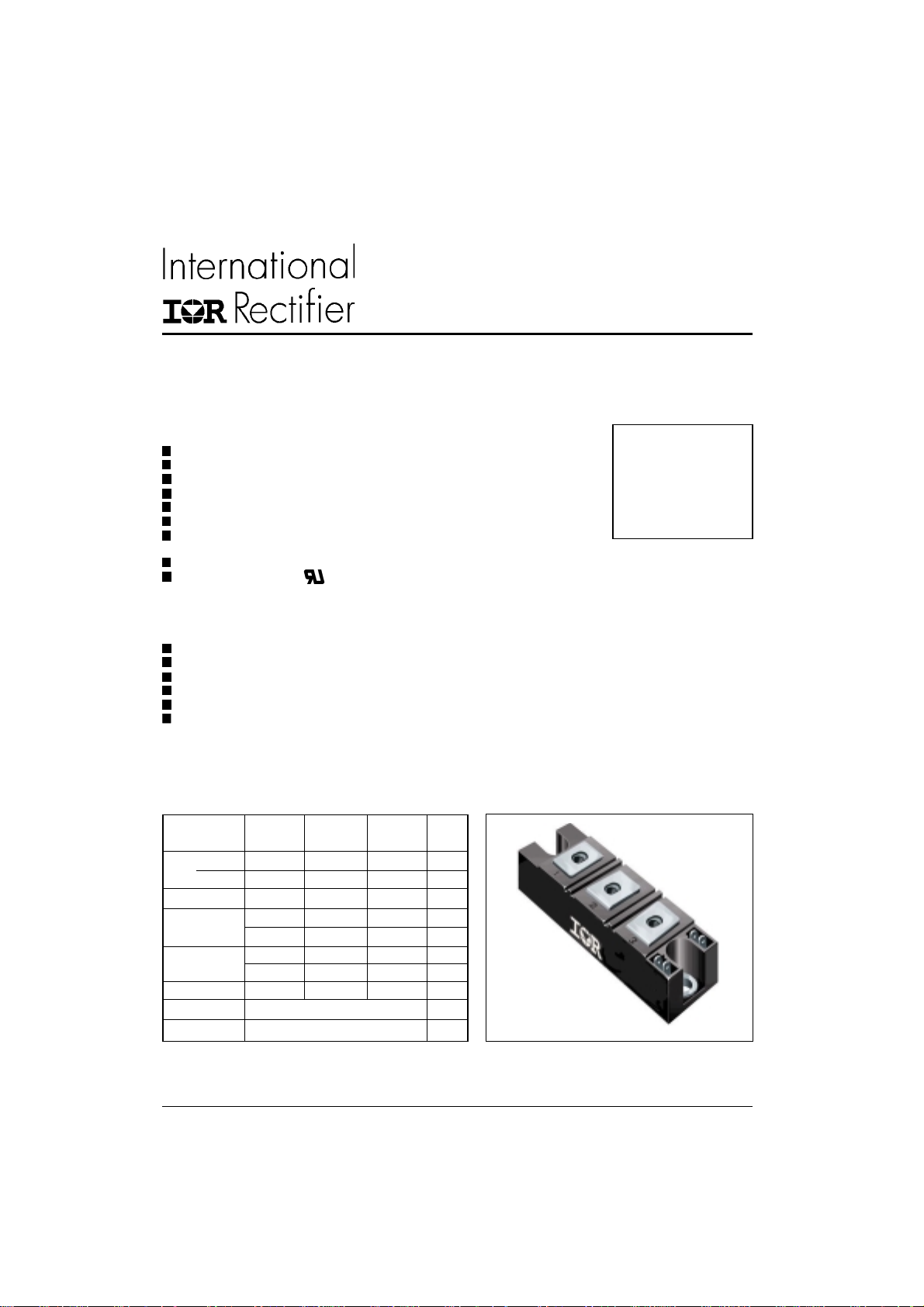
SERIES
IRK.136, .142, .162
THYRISTOR/DIODE and
THYRISTOR/THYRISTOR
Features
High Voltage
Electrically Isolated by DBC Ceramic ( Al2O3)
3500 V
Industrial Standard Package
High Surge Capability
Glass Passivated Chips
Modules uses High Voltage Power thyristor/diodes
in three Basic Configurations
Simple Mounting
UL E78996 approved
Isolating Voltage
RMS
Applications
DC Motor Control and Drives
Battery Charges
Welders
Power Converters
Lighting Control
Heat and Temperature Control
NEW INT-A-pak Power Modules
135 A
140 A
160 A
Major Ratings and Characteristics
Parameters IRK.136.. IRK.142.. IRK.162.. Units
I
T(AV)
@ T
C
I
T(RMS)
I
@ 50Hz 3200 4500 4870 A
TSM
@ 60Hz 3360 4712 5100 A
I2t @ 50Hz 51.5 102 119 KA2s
@ 60Hz 47 92.5 108 KA2s
2
I
√t 515.5 1013 1190 KA2√s
V
RRM
TJrange - 40 to 125 °C
www.irf.com
135 140 160 A
85 85 85 °C
300 310 355 A
400 to 1600 V
CASE STYLE NEW INT-A-PAK
1
IRK.136, .142, .162 Series
Bulletin I27117 rev. C 03/02
Electrical Specifications
Voltage Ratings
Type number Voltage V
Code peak reverse voltage peak reverse voltage @ 125°C
IRK.136 04 400 500 50
IRK.142 08 800 900
IRK.162 12 1200 1300
14 1400 1500
16 1600 1700
Forward Conduction
Parameter IRK.136 IRK.142 IRK.162 Units Conditions
Max. average on-state current 135 140 160 A 180° conduction, half sine wave
I
T(AV)
@ Case temperature 85 85 85 °C
I
Max. RMS on-state current 300 310 355 A as AC switch
T(RMS)
Maximum peak, one-cycle 3200 4500 4870 A t = 10ms No voltage
I
TSM
on-state, non-repetitive 3360 4712 5100 t = 8.3ms reapplied
surge current 2700 3785 4100 t = 10ms 100% V
2
I
t Maximum I2t for fusing 51.5 102 119 KA2s t = 10ms No voltage Initial TJ = TJ max.
2
√t Maximum I2√t for fusing 515.5 1013 1190 KA2√s t = 0.1 to 10ms, no voltage reapplied
I
V
Low level value of threshold 0.86 0.83 0.8 V (16.7% x π x I
(TO)1
T
voltage
High level value of threshold 1.05 1 0.98 (I > π x I
V
(TO)2
T
voltage
Low level value on-state 2.02 1.78 1.67 mΩ (16.7% x π x I
r
t1
slope resistance
High level value on-state 1.65 1.43 1.38 (I > π x I
r
t2
slope resistance
Maximum forward voltage drop 1.57 1.55 1.54 V I
V
TM
, Maximum repetitive V
RRM/VDRM
, Maximum non-repetitive I
RSM/VDSM
VVm A
2800 3963 4300 t = 8.3ms reapplied Sine half wave,
47 92.5 108 t = 8.3ms reapplied
36.5 71.6 84 t = 10ms 100% V
33.3 65.4 76.7 t = 8.3ms reapplied
(AV)
T
(AV)
T
= π x I
TM
RRM
RRM
< I < π x I
T(AV)
T(AV)
), @ TJ max.
< I < π x I
(AV)
T
T
), @ TJ max.
, TJ = 25°C, 180°conduction
T(AV)
RRM / IDRM
(AV)
), @ TJ max.
), @ TJ max.
Maximum holding current 200 mA Anode supply = 6V initial IT = 30A, TJ = 25°C
I
H
Maximum latching current 400 mA Anode supply = 6V resistive load = 1Ω
I
L
Gate pulse: 10V, 100µs, T
Switching
t
Typical delay time 1 TJ = 25oC Gate Current=1A dIg/dt=1A/µs
gd
tgrTypical rise time 2 µs TJ = 25oC Vd=0,67% V
tqTypical turn-off time 50 - 200 I
= 300 A; -dI/dt = 15 A/µs; T
TM
V
= 50 V; dV/dt = 20 V/µs; Gate 0 V, 100Ω
r
2
= 25°C
J
DRM
= TJ max
J
www.irf.com
IRK.136, .142, .162 Series
Bulletin I27117 rev. C 03/02
Blocking
I
Maximum peak reverse and 50 mA TJ = 125oC
RRM
off-state leakage current
I
DRM
RMS isolation voltage 3500 V 50Hz, circuit to base, all terminals shorted, t = 1s
V
INS
dV/dt critical rate of rise of off-state voltage 1000 V/µs T
Triggering
Parameter IRK.136 IRK.142 IRK.162 Units Conditions
P
Max. peak gate power 12 W tp ≤ 5ms, T
GM
Max. average gate power 3 W f=50Hz, TJ = TJ max.
P
G(AV)
Max. peak gate current 3 A tp ≤ 5ms, T
I
GM
Max. peak negative 10 V
-V
GT
gate voltage
V
Max. required DC gate 4 V TJ = - 40° C Anode supply = 6V, resistive
GT
voltage to trigger 2.5 T
1.7 T
I
Max. required DC gate 270 TJ = - 40° C Anode supply = 6V, resistive
GT
current to trigger 150 mA T
80 T
V
Max. gate voltage 0.3 V @ TJ = TJ max., rated V
GD
that will not trigger
I
Max. gate current 10 m A
GD
that will not trigger
di/
Max. rate of rise of 300 A/µs @ TJ = TJ max., I
dt
turned-on current
= TJ max., exponential to 67% rated V
J
= TJ max.
J
= TJ max.
J
= 25°C load; Ra = 1Ω
J
= TJ max.
J
= 25°C load; Ra = 1Ω
J
= TJ max.
J
= 400A rated V
TM
DRM
applied
DRM
DRM
applied
Thermal and Mechanical Specifications
Parameter IRK.136 IRK.142 IRK.162 Units Conditions
TJMax. junction operating -40 to 125 °C
temperature range
T
Max. storage temperature -40 to 150 °C
stg
range
R
Max. thermal resistance, 0.18 0.18 0.16 K/W DC operation, per junction
thJC
junction to case
R
Max. thermal resistance, 0.05 K/W Mounting surface smooth, flat and greased
thCS
case to heatsink Per module
T Mounting IAP to heatsink 4 to 6 Nm
torque ± 10% busbar to IAP 4 to 6
wt Approximate weight 200 (7.1) g(oz)
Case Style New Int-A-Pak
A mounting compound is recommended and
the torque should be rechecked after a period
of 3 hours to allow for the spread of the
compound. Lubricated threads.
∆R Conduction (per Junction)
(The following table shows the increment of thermal resistance R
Devices Units
Sinusoidal conduction @ TJ max. Rectangular conduction @ TJ max.
o
180o120
o
90
IRK.136 0.007 0.01 0.013 0.0155 0.017 0.009 0.012 0.014 0.015 0.017
IRK.142 0.0019 0.0019 0.0020 0.0020 0.0021 0.0018 0.0022 0.0023 0.0023 0.0020 K/W
IRK.162 0.0030 0.0031 0.0032 0.0033 0.0034 0.0029 0.0036 0.0039 0.0041 0.0040
when devices operate at different conduction angles than DC)
thJC
o
60
o
30
180
o
120
o
90
o
o
60
www.irf.com
o
30
3
IRK.136, .142, .162 Series
Bulletin I27117 rev. C 03/02
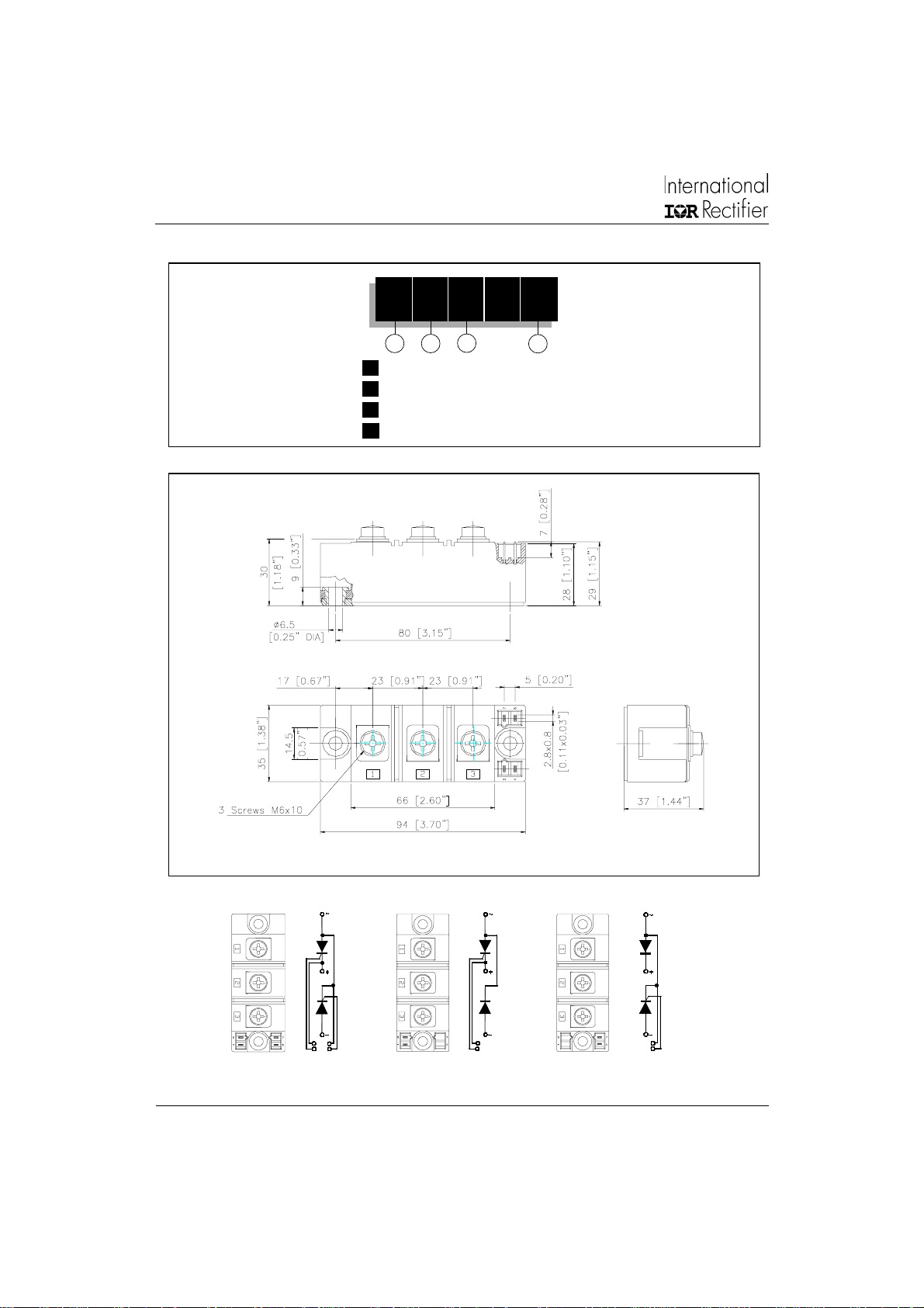
Ordering Information Table
Device Code
IRK T 162 / 16
Outline Table
1 2
3
4
1 - Module Type
2 - Circuit Configuration
3 - Current Rating: I
T(AV)
4 - Voltage Code: Code x 100 = V
RRM
Dimensions are in millimeters and [inches]
IRKT IRKH IRKL
1
2
3
5
7
6
4
NOTE: To order the Optional Hardware see Bulletin I27900
1
2
3
5
4
4
1
2
3
7
6
www.irf.com
IRK.136, .142, .162 Series
Bulletin I27117 rev. C 03/02
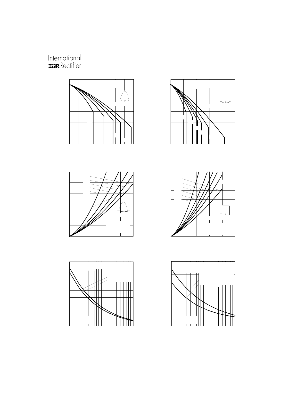
130
120
110
IRK.136.. Series
R (D C ) = 0.18 K /W
thJC
Conduction Angle
100
90
80
30
60
90
120
180
70
Maximum Allowable Case Temperature ( C)
0 20 40 60 80 100 120 140
Average Forward Current (A)
Fig. 1 - Current Ratings Characteristics
300
180
250
120
90
60
RMS Limit
30
Conduction Angle
IRK.136.. Series
Per Junction
T = 125 C
J
200
150
100
50
0
Maximum Average On-state Power Loss (W)
0 306090120150
Average On-state Current (A)
Fig. 3 - On-State Power Loss Characteristics
130
120
IRK.136.. Series
R (DC ) = 0.18 K/W
thJC
110
Conduction Period
100
30
90
60
90
80
70
Maximum Allowable Case Temperature ( C)
0 50 100 150 200 250
120
180
Average On-state Current (A)
Fig. 2 - Current Ratings Characteristics
350
DC
300
180
120
250
90
60
30
200
150
100
50
0
Maximum Average On-state Power Loss (W)
0 50 100 150 200 250
Conduction Period
IRK.136.. Series
Per Junction
T = 125 C
J
Average On-state Current (A)
Fig. 4 - On-State Power Loss Characteristics
DC
RMS Limit
3000
At Any Rated Load Condition And With
Rated V A pplied Following Surge.
2800
2600
2400
RRM
Initial T = 12 5 C
@ 60 Hz 0.0083 s
@ 50 Hz 0.0100 s
2200
2000
1800
1600
IRK.136.. Series
1400
Peak Half Sine W a ve On -state Curren t (A)
Per Junction
1200
110100
Number Of Equal Amplitude Half Cycle Current Pulses (N)
Fig.5 - Maximum Non-Repetitive Surge Current
www.irf.com
3500
J
3000
2500
Maximum Non Repetitive Surge Current
Vers us Pulse Train D uration. Control
Of Conduction May Not Be Maintained.
Initial T = 125 C
No Voltage Reapplied
Rated V Reapplied
J
RRM
2000
1500
IRK.136.. Series
Peak Half Sine Wave On-state Current (A)
Per Junction
1000
0.01 0.1 1
Pulse Train Duration (s)
Fig. 6 - Maximum Non-Repetitive Surge Current
5

IRK.136, .142, .162 Series
Bulletin I27117 rev. C 03/02
450
400
350
300
250
Conduction Angle
180
120
90
60
30
200
150
100
50
Maximum Total On -state Power Loss (W )
0
0 50 100 150 200 250 300
IRK.136.. Series
Per Module
Total RMS Output Current (A)
Fig.7 - On State Power Loss Characteristics
1000
900
800
700
600
500
180
(Sine)
180
(Rect)
400
300
200
Maximum Total Power Loss (W)
100
0
0 55 110 165 220 275
2 x IRK.136.. Series
Single Phase Bridge
Connected
T = 125 C
J
Total Output Current (A)
Fig.8 - On State Power Loss Characteristics
T = 125 C
J
0
0
.
.
1
0
2
8
K
0
/
.
W
1
6
K
/
W
0
.
2
5
K
/
W
0
.
4
K
/
W
0
.
6
K
/
W
1
K
/
W
R
0
.
K
0
t
h
4
/
S
W
K
A
/
=
W
0
.
0
1
K
/
W
D
e
l
t
a
R
0255075100125
Maximum Allowable Ambient Temperature ( C)
R
0
t
.
h
0
S
4
A
K
=
0
.
0
.
1
2
K
0
.
2
K
/
W
0
.
3
5
K
0
.
6
K
/
/
W
0
8
K
/
W
/
W
/
W
W
0
.
0
1
K
/
W
D
e
l
t
a
R
0255075100125
Maximum Allowable Ambient Temperature ( C)
1500
R
t
h
S
1200
900
120
(Rec t)
600
3 x IRK.136.. Series
300
Maximum Total Power Loss (W)
0
0 100 200 300 400
Three Phase Bridge
Connected
T = 125 C
J
Total O utput Current (A)
A
=
0
.
0
4
0
.
0
8
0
.
1
K
0
.
1
6
K
0
.
2
5
0
.
4
K
1
K
/
W
K
/
K
/
W
/
W
K
/
/
W
W
/
W
W
D
e
l
t
a
R
0 255075100125
Maximum Allowable Ambient Temperature ( C)
Fig.9- On State Power Loss Characteristics
6
www.irf.com

IRK.136, .142, .162 Series
Bulletin I27117 rev. C 03/02
130
IRK.142.. Series
R (D C ) = 0.18 K /W
120
thJC
110
Conduction Angle
100
90
80
70
Maximum Allowable Case Temperature ( C)
0306090120150
30
60
90
120
180
Average Forward Current (A)
Fig. 10 - Current Ratings Characteristics Fig. 11 - Current Ratings Characteristics
250
180
120
200
90
60
30
150
RMS Limit
100
Conduction Angle
50
IRK.142.. Series
Per Junction
T = 125 C
0
Maximum Average On-state Power Loss (W)
0306090120150
J
Average On-state Current (A)
Fig. 12 - On-State Power Loss Characteristics
4500
At Any Rated Load Condition And With
Rated V A pplied Following Surge.
4000
3500
RRM
Initial T = 125 C
J
@ 60 Hz 0.0083 s
@ 50 Hz 0.0100 s
130
120
IRK.142.. Series
R (DC) = 0.18 K/W
thJC
110
100
90
30
60
90
120
80
70
Maximum Allowable Case Temperature ( C)
0 50 100 150 200 250
Average On-state Current (A)
350
300
250
DC
180
120
90
60
30
200
RMS Limit
150
100
Conduction Period
IRK.142.. Series
50
0
Maximum Average On-state Power Loss (W)
0 50 100 150 200 250
Per Junction
T = 125 C
J
Average On-state Current (A)
Fig. 13 - On-State Power Loss Characteristics
5000
4500
4000
Maximum Non Repetitive Surge Current
Versus Pulse Train Duration. Control
Of Co nduction May Not Be M aintained .
No Voltage Reapplied
Rated V Rea pplied
3500
3000
3000
2500
2000
IRK.142.. Series
Peak Half Sine W a ve On-stat e C urren t (A)
Per Junction
1500
110100
Num b er Of Equ al Amplitud e H alf Cycle Current Pulses (N)
Fig.14 - Maximum Non-Repetitive Surge Current Fig. 15 - Maximum Non-Repetitive Surge Current
2500
2000
IRK.142.. Series
Peak Half Sine W ave On-sta te Curren t (A)
Per Junction
1500
0.01 0.1 1
Pulse Train Duration (s)
Conduction Period
180
DC
Initial T = 125 C
J
RRM
www.irf.com
7

IRK.136, .142, .162 Series
Bulletin I27117 rev. C 03/02
400
180
300
120
90
60
30
200
Conduction Angle
100
Maximum Total On-state Power Loss (W )
0
0 50 100 150 200 250 300
IRK.142.. Series
Per Module
T = 125 C
Total RMS Output Current (A)
Fig.16 - On State Power Loss Characteristics
1000
800
600
400
180
(Sine)
180
(Rect)
0
0
.
1
.
1
2
6
K
K
/
/
W
W
0
.
2
5
K
/
W
0
.
4
K
/
W
0
.
6
K
/
W
1
K
/
W
J
R
0
0
.
t
.
0
h
0
4
S
8
A
K
K
=
/
/
W
W
0
.
0
1
K
/
W
D
e
l
t
a
R
0255075100125
Maximum Allowable Ambient Temperature ( C)
R
0
.
t
0
h
4
S
K
A
0
.
0.
1
0
.
1
0
.
2
5
/
W
0
8
K
/
W
2
K
/
W
6
K
/
W
K
/
W
=
0
.
0
1
K
/
W
D
e
l
t
a
R
200
Maximum Total Power Loss (W)
0
0 100 200 300
2 x IRK.142.. Series
Single Phase Bridge
Connected
T = 125 C
J
Total O utput Current (A)
0
.
6
K
/
W
0255075100125
Maximum Allowable Ambient Temperature ( C)
Fig.17 - On State Power Loss Characteristics
1600
R
t
h
S
A
/
W
=
0
.
0
2
K
/
W
-
D
e
l
t
a
R
1200
120
(Rect)
800
400
Maximum Total Power Loss (W)
0
0 50 100 150 200 250 300 350 400 450
3 x IRK.142.. Series
Three Phase Bridge
Connected
T = 125 C
J
Total Output Current (A)
0
.
0
4
K
0
.
0
6
K
/
W
0
.
0
8
K
/
W
0
.
1
K
/
W
0
.
1
6
K
/
W
0
.
2
K
/
W
0255075100125
Maximum Allowable Ambient Temperature ( C)
Fig.18- On State Power Loss Characteristics
8
www.irf.com

IRK.136, .142, .162 Series
Bulletin I27117 rev. C 03/02
130
120
IRK.162.. Series
R (DC ) = 0.16 K/W
thJC
110
Conduction Angle
100
90
80
70
Maximum Allowable Case Temperature ( C)
0306090120150180
30
60
90
120
180
Average Forward Current (A)
Fig. 19 - Current Ratings Characteristics Fig. 20 - Current Ratings Characteristics
400
IRK.162.. Series
Per Junction
350
T = 125 C
J
300
250
200
150
180
120
90
60
30
RMS Limit
100
50
0
Maximum Average On-state Power Loss (W)
0 20406080100120140160180
Conduction Angle
Average On-state Current (A)
130
120
IRK.162.. Series
R (DC ) = 0.16 K/W
thJC
110
100
90
30
60
80
70
60
Maximum Allowable Case Temperature ( C)
0 50 100 150 200 250 300
90
120
Average On-state Current (A)
400
350
300
250
200
DC
180
120
90
60
30
RMS Limit
150
100
50
0
Maximum Average On-state Power Loss (W)
0 306090120150180210240270
Average On-state Current (A)
Conduction Period
180
Conduction Period
DC
IRK.162.. Series
Per Junction
T = 125 C
J
Fig. 21 - On-State Power Loss Characteristics
4500
At Any Rated Load Condition And With
Rate d V Applied Follow ing Surge.
4000
RRM
Initial T = 125 C
@ 60 Hz 0.0083 s
3500
@ 50 Hz 0.0100 s
3000
2500
2000
IRK.162.. Series
Peak Half Sine Wave On-state Current (A)
Per Junction
1500
110100
Num ber O f Equa l Am plitude Half Cy cle C urrent P ulses (N)
Fig.23 - Maximum Non-Repetitive Surge Current Fig. 24 - Maximum Non-Repetitive Surge Current
www.irf.com
Fig. 22 - On-State Power Loss Characteristics
5000
J
4500
4000
Maximum Non Repetitive Surge Current
Versus Pulse Train Duration. Control
Of Co nduction May Not Be M ainta ined .
In itial T = 1 25 C
No Voltage Reapplied
Rated V Reapplied
J
RRM
3500
3000
2500
2000
IRK.162.. Series
Per Junction
Peak Half Sine Wave On-state Current (A)
1500
0.01 0.1 1
Pulse Train Duration (s)
9

IRK.136, .142, .162 Series
Bulletin I27117 rev. C 03/02
600
500
400
300
Conduction Angle
180
120
90
60
30
200
IRK.162.. Series
100
Maximum Total On-state Power Loss (W)
0
0 100 200 300 400
Per Module
Total RMS Output Current (A)
Fig.25 - On State Power Loss Characteristics
900
800
700
600
500
400
180
(Sine)
180
(Rect)
300
200
Maximum Total Power Loss (W)
100
0
0 50 100 150 200 250 300
2 x IRK.162.. Series
Single Phase Bridge
Connected
T = 125 C
J
Tota l Output Current (A)
Fig.26 - On State Power Loss Characteristics
T = 125 C
J
0
.
0
6
K
0
.
0
8
K
/
W
0
.
1
K
/
W
0
.
1
6
K
/
W
0
.
2
K
/
W
h
0
S
4
A
K
=
/
/
W
W
0
.
0
2
K
/
W
D
e
l
t
a
R
R
0
t
.
0255075100125
Maximum Allowable Ambient Temperature ( C)
0
.
0
8
0
.
1
2
K
0
.
2
K
/
0
.
3
K
/
0
.
4
K
/
0
.
6
K
/
W
1
K
/
W
R
t
K
/
W
W
W
W
h
S
/
A
W
=
0
.
0
4
K
/
W
D
e
l
t
a
R
0255075100125
Maximum Allowable Ambient Temperature ( C)
10
1500
1250
1000
750
500
120
(Rect)
3 x IRK.162.. Series
Three Phase Bridge
250
Maximum Total Power Loss (W)
0
0 50 100 150 200 250 300 350 400 450
Connected
T = 125 C
J
Total Output Current (A)
Fig.27- On State Power Loss Characteristics
R
0
0
.
0
8
K
/
0
.
1
2
K
/
0
.
2
K
/
W
0
.
3
K
/
W
0
.
6
K
/
.
W
W
0
t
h
4
S
K
A
/
W
=
0
.
0
2
K
/
W
W
D
e
l
t
a
R
0255075100125
Maximum Allowable Ambient Temperature ( C)
www.irf.com
IRK.136, .142, .162 Series
0
0
0
Bulletin I27117 rev. C 03/02
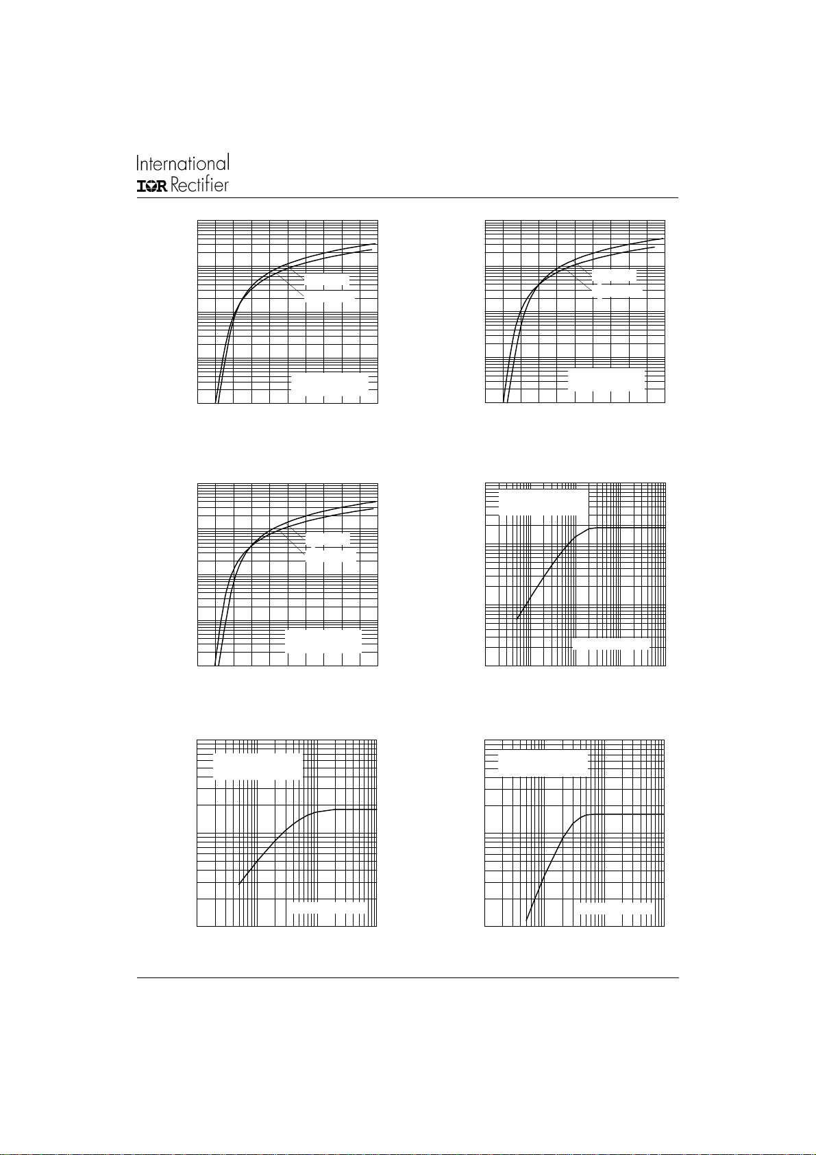
10000
1000
T = 25˚C
J
T = 125˚C
100
J
10
Instantaneous On-state Current (A)
1
012345
IRK.136.. Series
Per Junction
Instantaneous On-state Voltage (V)
Fig.28 - On State Voltage Drop Characteristics
10000
1000
T = 25˚C
J
T = 125˚C
J
100
10
IRK.162.. Series
Instantaneous On-state Current (A)
1
012345
Per Junction
Instantaneous On-state Voltage (V)
10000
1000
T = 25˚C
J
T = 125˚C
J
100
10
IRK.142.. Series
Instantaneous On-state Current (A)
1
012345
Per Junction
Instantaneous On-state Voltage (V)
Fig.29 - On State Voltage Drop Characteristics
1
thJC
Steady State Value
(DC Operation)
0.1
0.01
Transient Thermal Impedance Z
.001
0.001 0.01 0.1 1 10
IRK.136.. Series
Square Wave Pulse Duration (s)
Fig.30 - On State Voltage Drop Characteristics
1
thJC
Steady State Value
(DC Operation)
0.1
Transient Thermal Impedance Z
.01
0.01 0.1 1 10
Square Wave Pulse Duration (s)
Fig.32 - Thermal Impedance ZthJC Characteristics
www.irf.com
IRK.142.. Series
Fig.31 - Thermal Impedance ZthJC Characteristics
1
thJC
Steady State Value
(DC Operation)
0.1
Transient Thermal Impedance Z
.01
0.01 0.1 1 10
IRK.162.. Series
Square Wave Pulse Duration (s)
Fig.33 - Thermal Impedance ZthJC Characteristics
11

IRK.136, .142, .162 Series
Bulletin I27117 rev. C 03/02
100
Rectangular gate pulse
a)Recommended load line for
rated d i/dt: 20 V, 20 ohms
tr = 0.5 s, tp >= 6 s
b)R eco m m en ded loa d line for
<= 30% rated di/dt: 15 V, 40 ohm s
10
tr = 1 s, tp >= 6 s
1
Instantaneous Gate Voltage (V)
VGD
IG D
0.1
0.001 0.01 0.1 1 10 100 1000
(a)
(b)
TJ = -40 C
TJ = 25 C
TJ = 125 C
IRK.136..142..162.. Series
Instan taneous Gate Current (A)
Fig. 34 - Gate Characteristics
(1) PGM = 200 W, tp = 300 s
(2) PGM = 60 W, tp = 1 ms
(3) PGM = 30 W, tp = 2 ms
(4) PGM = 12 W, tp = 5 ms
(4) (3)
Frequency Limited by PG(AV)
(2) (1)
Data and specifications subject to change without notice.
This product has been designed and qualified for Multiple Level.
Qualification Standards can be found on IR's Web site.
IR WORLD HEADQUARTERS: 233 Kansas St., El Segundo, California 90245, USA Tel: (310) 252-7105
TAC Fax: (310) 252-7309
Visit us at www.irf.com for sales contact information. 03/02
12
www.irf.com
 Loading...