

Vishay IRFZ48RS, IRFZ48RL, SiHFZ48RS, SiHFZ48RL Data Sheet
N-Channel MOSFET
G
D
S
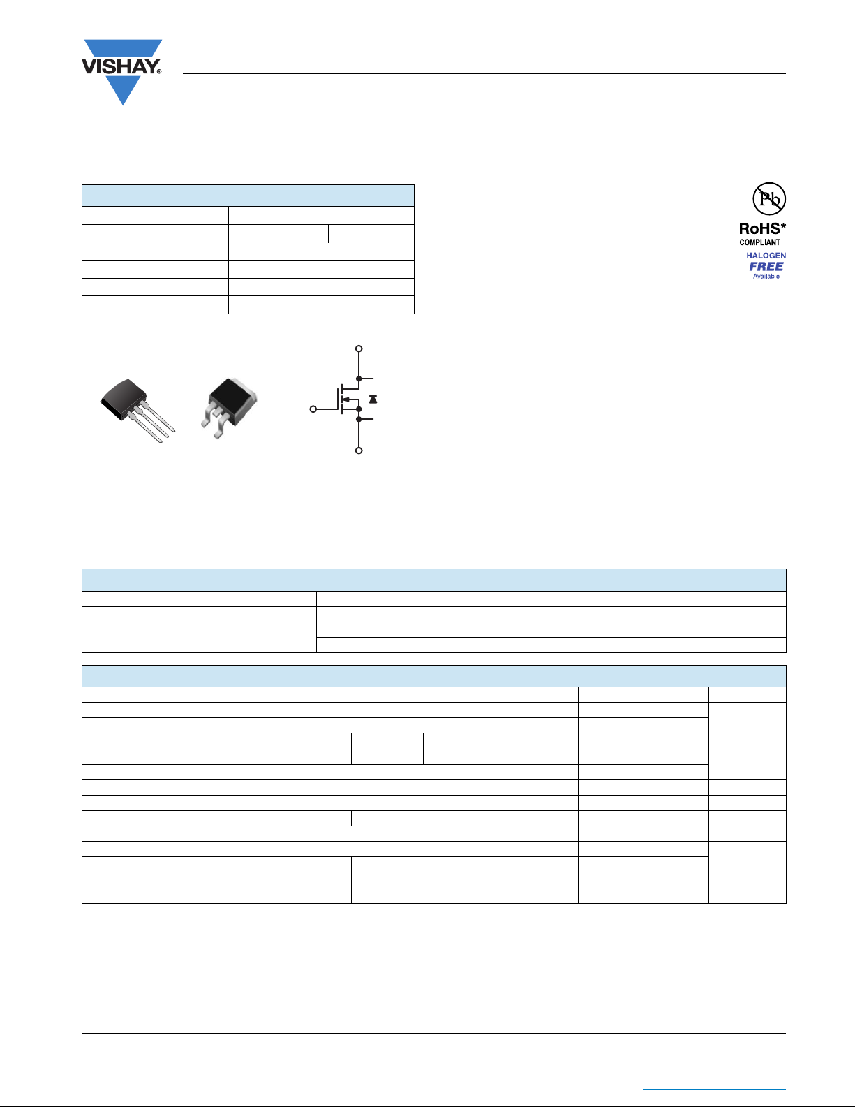
D2PAK (TO-263)
G
D
S
I2PAK (TO-262)
G
D
S
IRFZ48RS, IRFZ48RL, SiHFZ48RS, SiHFZ48RL
Vishay Siliconix
Power MOSFET
PRODUCT SUMMARY
VDS (V) 60
()V
R
DS(on)
Q
(Max.) (nC) 110
g
(nC) 29
Q
gs
Q
(nC) 36
gd
Configuration Single
= 10 V 0.018
GS
FEATURES
• Halogen-free According to IEC 61249-2-21
Definition
• Advanced Process Technology
• Dynamic dV/dt
• 175 °C Operating Temperature
•Fast Switching
• Fully Avalanche Rated
• Drop in Replacement of the IRFZ48, SiHFZ48 for
Linear/Audio Applications
• Compliant to RoHS Directive 2002/95/EC
DESCRIPTION
Advanced Power MOSFETs from Vishay utilize advanced
processing techniques to achieve extremely low
on-resistance per silicon area. This benefit, combined with
the fast switching speed and ruggedized device design that
Power MOSFETs are well known for, provides the designer
with an extremely efficient and reliable device for use in a
wide variety of applications.
2
The D
PAK is a surface mount power package capable of
accommodating die sizes up to HEX-4. It provides the
highest power capability and the lowest possible
on-resistance in any existing surface mount package. The
2
D
PAK is suitable for high current applications because of
its low internal connection resistance and can dissipate up
to 2 W in a typical surface mount application.
ORDERING INFORMATION
Package D2PAK (TO-263) I2PAK (TO-262)
Lead (Pb)-free and Halogen-free SiHFZ48RS-GE3 -
Lead (Pb)-free
IRFZ48RSPbF IRFZ48RLPbF
SiHFZ48RS-E3 SiHFZ48RL-E3
ABSOLUTE MAXIMUM RATINGS (TC = 25 °C, unless otherwise noted)
PARAMETER SYMBOL LIMIT UNIT
Drain-Source Voltage V
Gate-Source Voltage V
T
= 25 °C
Continuous Drain Current
Pulsed Drain Current
Linear Derating Factor
Single Pulse Avalanche Energy
Maximum Power Dissipation T
Peak Diode Recovery dV/dt
Operating Junction and Storage Temperature Range T
Soldering Recommendations (Peak Temperature)
Mounting Torque 6-32 or M3 screw
Notes
a. Repetitive rating; pulse width limited by maximum junction temperature (see fig. 11).
b. V
= 25 V, Starting TJ = 25 °C, L = 22 μH, Rg = 25 , IAS = 72 A (see fig. 12).
DD
c. ISD 72 A, dI/dt 200 A/μs, VDD VDS, TJ 175 °C.
d. 1.6 mm from case.
e. Current limited by the package, (die current = 72 A).
* Pb containing terminations are not RoHS compliant, exemptions may apply
Document Number: 91296
S11-1054-Rev. C, 30-May-11 1
THE PRODUCTS DESCRIBED HEREIN AND THIS DOCUMENT ARE SUBJECT TO SPECIFIC DISCLAIMERS, SET FORTH AT
e
a, e
b, e
c, e
VGS at 10 V
d
This document is subject to change without notice.
C
T
= 100 °C
C
= 25 °C P
C
for 10 s
www.vishay.com
DS
GS
I
D
IDM
E
AS
D
dV/dt
, T
J
stg
60
± 20
50
50
290
1.3
100
190
4.5
- 55 to + 175
d
300
10
1.1
www.vishay.com/doc?91000
V
A
W/°C
mJ
W
V/ns
°C
lbf · in
N · m
IRFZ48RS, IRFZ48RL, SiHFZ48RS, SiHFZ48RL
Vishay Siliconix
THERMAL RESISTANCE RATINGS
PARAMETER SYMBOL TYP. MAX. UNIT
Maximum Junction-to-Ambient R
Maximum Junction-to-Case (Drain) R
thJA
thCS
thJC
SPECIFICATIONS (TJ = 25 °C, unless otherwise noted)
PARAMETER SYMBOL TEST CONDITIONS MIN. TYP. MAX. UNIT
Static
Drain-Source Breakdown Voltage V
V
Temperature Coefficient VDS/TJ Reference to 25 °C, ID = 1 mA
DS
Gate-Source Threshold Voltage V
Gate-Source Leakage I
Zero Gate Voltage Drain Current I
Drain-Source On-State Resistance R
Forward Transconductance g
Dynamic
Input Capacitance C
Reverse Transfer Capacitance C
Total Gate Charge Q
Gate-Drain Charge Q
Turn-On Delay Time t
Rise Time t
Turn-Off Delay Time t
Fall Time t
Internal Drain Inductance L
Internal Source Inductance L
Drain-Source Body Diode Characteristics
Continuous Source-Drain Diode Current I
Pulsed Diode Forward Current
a
Body Diode Voltage V
Body Diode Reverse Recovery Time t
Body Diode Reverse Recovery Charge Q
Forward Turn-On Time t
Notes
a. Repetitive rating; pulse width limited by maximum junction temperature (see fig. 11).
b. Pulse width 300 μs; duty cycle 2 %.
c. Current limited by the package, (die current = 72 A).
DS
GS(th)
V
GSS
DSS
VGS = 10 V ID = 43 A
DS(on)
fs
iss
- 1300 -
oss
- 190 -
rss
g
--29
gs
--36
gd
d(on)
r
- 210 -
d(off)
- 250 -
f
D
V
V
GS
R
g
Between lead,
6 mm (0.25") from
package and center of
S
S
die contact
MOSFET symbol
showing the
integral reverse
I
SM
SD
rr
rr
on
p - n junction diode
TJ = 25 °C, IF = 72 A, dI/dt = 100 A/μs
-62
0.50 -
°C/WCase-to-Sink, Flat, Greased Surface R
-0.8
VGS = 0 V, ID = 250 μA 60 - - V
c
-0.60-V/°C
VDS = VGS, ID = 250 μA 2.0 - 4.0 V
= ± 20 V - - ± 100 nA
GS
VDS = 60 V, VGS = 0 V - - 25
= 48 V, VGS = 0 V, TJ = 150 °C - - 250
DS
VDS = 25 V, ID = 43 A
VGS = 0 V,
V
= 25 V,
DS
f = 1.0 MHz, see fig. 5
b
b
c
- - 0.018
27 - - S
- 2400 -
- - 110
= 72 A, VDS = 48 V,
I
= 10 V
D
see fig. 6 and 13
b, c
-8.1-
= 30 V, ID = 72 A,
V
DD
= 9.1 , RD = 0.34 , see fig. 10
G
G
TJ = 25 °C, IS = 72 A, VGS = 0 V
b, c
D
S
D
S
b
b, c
- 250 -
-4.5-
-7.5-
--50
c
- - 290
--2.0V
- 120 180 ns
- 0.50 0.80 μC
Intrinsic turn-on time is negligible (turn-on is dominated by LS and LD)
μA
pFOutput Capacitance C
nC Gate-Source Charge Q
ns
nH
A
www.vishay.com Document Number: 91296
2 S11-1054-Rev. C, 30-May-11
This document is subject to change without notice.
THE PRODUCTS DESCRIBED HEREIN AND THIS DOCUMENT ARE SUBJECT TO SPECIFIC DISCLAIMERS, SET FORTH AT
www.vishay.com/doc?91000
IRFZ48RS, IRFZ48RL, SiHFZ48RS, SiHFZ48RL
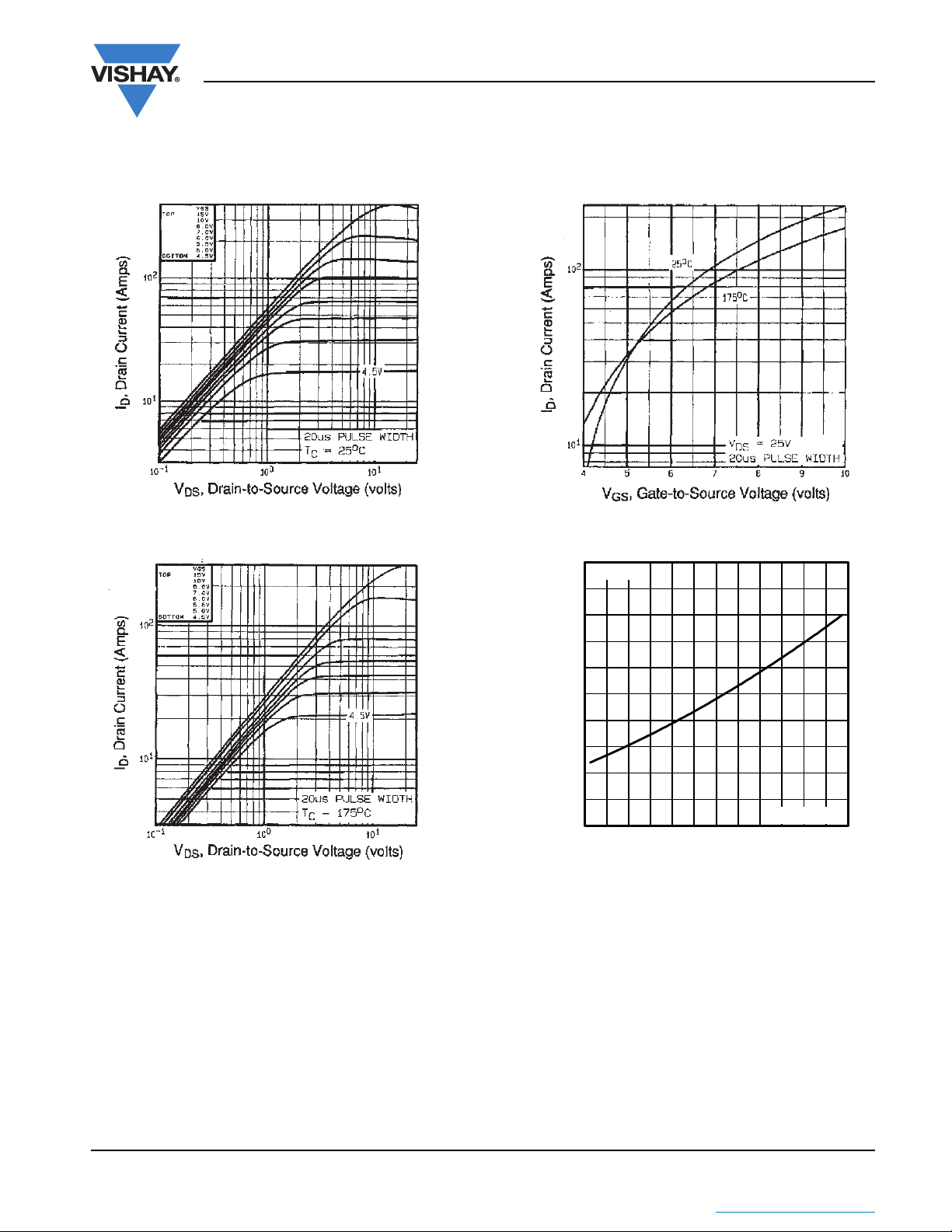
TYPICAL CHARACTERISTICS (25 °C, unless otherwise noted)
Vishay Siliconix
Fig. 1 - Typical Output Characteristics
Fig. 2 - Typical Output Characteristics
Fig. 3 - Typical Transfer Characteristics
2.5
2.0
1.5
1.0
(Normalized)
0.5
DS(on)
R , Drain-to-Source On Resistance
0.0
Fig. 4 - Normalized On-Resistance vs. Temperature
72A
I =
D
V =
GS
-60 -40 -20 0 20 40 60 80 100 120 140 160 180
T , Junction Temperature ( C)
J
°
10V
Document Number: 91296 www.vishay.com
S11-1054-Rev. C, 30-May-11 3
THE PRODUCTS DESCRIBED HEREIN AND THIS DOCUMENT ARE SUBJECT TO SPECIFIC DISCLAIMERS, SET FORTH AT
This document is subject to change without notice.
www.vishay.com/doc?91000
1
10
100
1000
0.1 1 10 100 1000
OPERATION IN THIS AREA LIMITED
BY R
DS(on)
Single Pulse
T T= 175 C
= 25 C
°
°
J
C
V , Drain-to-Source Voltage (V)
I , Drain Current (A)I , Drain Current (A)
DS
D
10us
100us
1ms
10ms
IRFZ48RS, IRFZ48RL, SiHFZ48RS, SiHFZ48RL
Vishay Siliconix
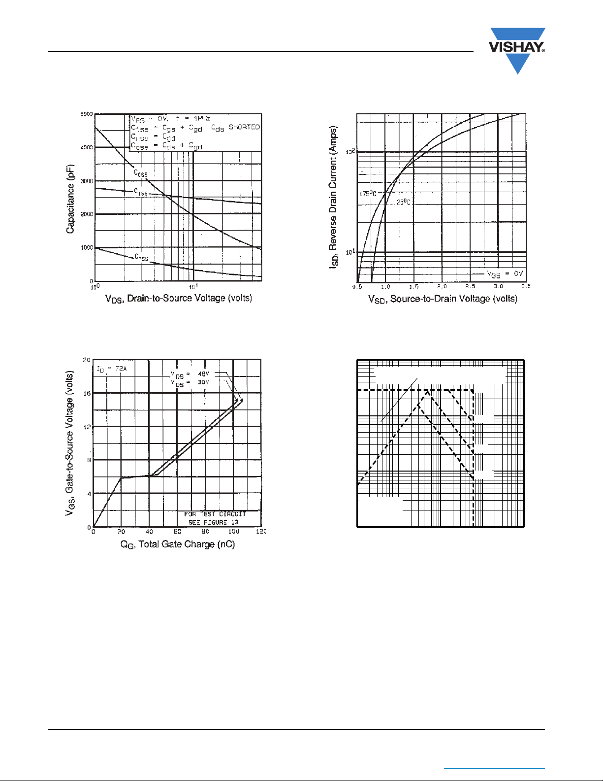
Fig. 5 - Typical Capacitance vs. Drain-to-Source Voltage
Fig. 6 - Typical Gate Charge vs. Gate-to-Source Voltage
Fig. 7 - Typical Source-Drain Diode Forward Voltage
Fig. 8 - Maximum Safe Operating Area
www.vishay.com Document Number: 91296
4 S11-1054-Rev. C, 30-May-11
THE PRODUCTS DESCRIBED HEREIN AND THIS DOCUMENT ARE SUBJECT TO SPECIFIC DISCLAIMERS, SET FORTH AT
This document is subject to change without notice.
www.vishay.com/doc?91000
 Loading...