

Vishay IRFZ44R, SiHFZ44R Data Sheet
N-Channel MOSFET
G
D
S
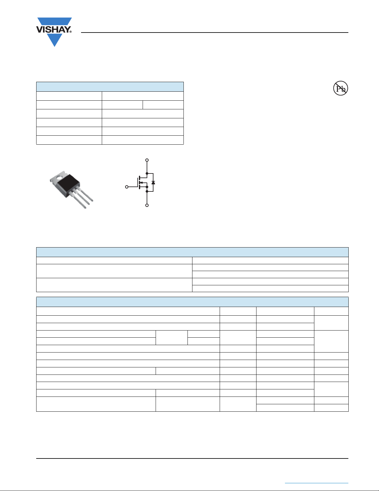
TO-220AB
G
D
S
Available
RoHS*
COMPLIANT
Power MOSFET
IRFZ44R, SiHFZ44R
Vishay Siliconix
PRODUCT SUMMARY
VDS (V) 60
(Ω)V
R
DS(on)
Q
(Max.) (nC) 67
g
Q
(nC) 18
gs
Q
(nC) 25
gd
Configuration Single
= 10 V 0.028
GS
FEATURES
• Advanced Process Technology
• Ultra Low On-Resistance
• Dynamic dV/dt Rating
• 175 °C Operating Temperature
•Fast Switching
• Fully Avalanche Rated
• Drop in Replacement of the IRFZ44, SiHFZ44 for
Linear/Audio Applications
• Compliant to RoHS Directive 2002/95/EC
DESCRIPTION
Advanced Power MOSFETs from Vishay utilize advanced
processing techniques to achieve extremely low
on-resistance per silicon area. This benefit, combined with
the fast switching speed and ruggedized device design that
Power MOSFETs are well known for, provides the designer
with an extremely efficient and reliable device for use in a
wide variety of applications.
The TO-220AB package is universally preferred for all
commercial-industrial applications at power dissipation
levels to approximately 50 W. The low thermal resistance
and low package cost of the TO-220AB contribute to its
wide acceptance throughout the industry.
ORDERING INFORMATION
Package TO-220AB
Lead (Pb)-free
SnPb
IRFZ44RPbF
SiHFZ44R-E3
IRFZ44R
SiHFZ44R
ABSOLUTE MAXIMUM RATINGS (TC = 25 °C, unless otherwise noted)
PARAMETER SYMBOL LIMIT UNIT
Drain-Source Voltage V
Gate-Source Voltage V
Continuous Drain Current
Continuous Drain Current
Pulsed Drain Current
Linear Derating Factor 1.0 W/°C
Single Pulse Avalanche Energy
Maximum Power Dissipation T
Peak Diode Recovery dV/dt
Operating Junction and Storage Temperature Range T
Soldering Recommendations (Peak Temperature)
Mounting Torque 6-32 or M3 screw
Notes
a. Repetitive rating; pulse width limited by maximum junction temperature (see fig. 11).
= 25 V, starting TJ = 25 °C, L = 44 μH, Rg = 25 Ω, IAS = 51 A (see fig. 12).
b. V
DD
≤ 51 A, dV/dt ≤ 250 A/μs, VDD ≤ VDS, TJ ≤ 175 °C.
c. I
SD
d. 1.6 mm from case.
e. Current limited by the package, (die current = 51 A).
* Pb containing terminations are not RoHS compliant, exemptions may apply
Document Number: 91292 www.vishay.com
S11-0517-Rev. B, 21-Mar-11 1
THE PRODUCT DESCRIBED HEREIN AND THIS DATASHEET ARE SUBJECT TO SPECIFIC DISCLAIMERS, SET FORTH AT
e
a
b
c
VGS at 10 V
d
This datasheet is subject to change without notice.
TC = 25 °C
T
= 100 °C 36
C
= 25 °C P
C
for 10 s 300
60
DS
± 20
GS
I
D
IDM 200
E
AS
D
dV/dt 4.5 V/ns
, T
J
stg
50
100 mJ
150 W
- 55 to + 175
10 lbf · in
1.1 N · m
www.vishay.com/doc?91000
V
A
°C
IRFZ44R, SiHFZ44R
D
S
G
S
D
G
Vishay Siliconix
THERMAL RESISTANCE RATINGS
PARAMETER SYMBOL TYP. MAX. UNIT
Maximum Junction-to-Ambient R
Maximum Junction-to-Case (Drain) R
thJA
thCS
thJC
-62
0.50 -
-1.0
°C/WCase-to-Sink, Flat, Greased Surface R
SPECIFICATIONS (TJ = 25 °C, unless otherwise noted)
PARAMETER SYMBOL TEST CONDITIONS MIN. TYP. MAX. UNIT
Static
Drain-Source Breakdown Voltage V
V
Temperature Coefficient ΔVDS/TJ Reference to 25 °C, ID = 1 mA - 0.060 - V/°C
DS
Gate-Source Threshold Voltage V
Gate-Source Leakage I
Zero Gate Voltage Drain Current I
Drain-Source On-State Resistance R
Forward Transconductance g
DS
GS(th)
V
GSS
DSS
V
DS(on)
fs
Dynamic
Input Capacitance C
Reverse Transfer Capacitance C
Total Gate Charge Q
Gate-Drain Charge Q
Turn-On Delay Time t
Rise Time t
Turn-Off Delay Time t
Fall Time t
Internal Drain Inductance L
Internal Source Inductance L
iss
- 920 -
oss
- 170 -
rss
g
--18
gs
--25
gd
d(on)
r
-45-
d(off)
-92-
f
D
S
Between lead,
6 mm (0.25") from
package and center of
die contact
Drain-Source Body Diode Characteristics
Continuous Source-Drain Diode Current I
Pulsed Diode Forward Current
a
Body Diode Voltage V
Body Diode Reverse Recovery Time t
Body Diode Reverse Recovery Charge Q
Forward Turn-On Time t
S
I
SM
SD
rr
rr
on
MOSFET symbol
showing the
integral reverse
p - n junction diode
Notes
a. Repetitive rating; pulse width limited by maximum junction temperature (see fig. 11).
b. Pulse width ≤ 300 μs; duty cycle ≤ 2 %.
c. Current limited by the package (die current = 51 A).
VGS = 0 V, ID = 250 μA 60 - - V
VDS = VGS, ID = 250 μA 2.0 - 4.0 V
= ± 20 - - ± 100 nA
GS
VDS = 60 V, VGS = 0 V - - 25
V
= 48 V, VGS = 0 V, TJ = 150 °C - - 250
DS
= 10 V ID = 31 A
GS
VDS = 25 V, ID = 31 A
VGS = 0 V,
V
= 25 V,
DS
f = 1.0 MHz, see fig. 5
b
b
--0.028Ω
15 - - S
- 1900 -
--67
V
GS
= 10 V
ID = 51 A, VDS = 48 V,
see fig. 6 and 13
b
-14-
= 30 V, ID = 51 A,
V
R
DD
= 9.1 Ω, RD = 0.55 Ω, see fig. 10
g
b
- 110 -
-4.5-
-7.5-
--50
- - 200
TJ = 25 °C, IS = 51 A, VGS = 0 V
TJ = 25 °C, IF = 51 A, dI/dt = 100 A/μs
b
--2.5
- 120 180
b
- 0.53 0.80
Intrinsic turn-on time is negligible (turn-on is dominated by LS and LD)
c
μA
pFOutput Capacitance C
nC Gate-Source Charge Q
ns
nH
A
V
ns
μC
www.vishay.com Document Number: 91292
2 S11-0517-Rev. B, 21-Mar-11
THE PRODUCT DESCRIBED HEREIN AND THIS DATASHEET ARE SUBJECT TO SPECIFIC DISCLAIMERS, SET FORTH AT
This datasheet is subject to change without notice.
www.vishay.com/doc?91000
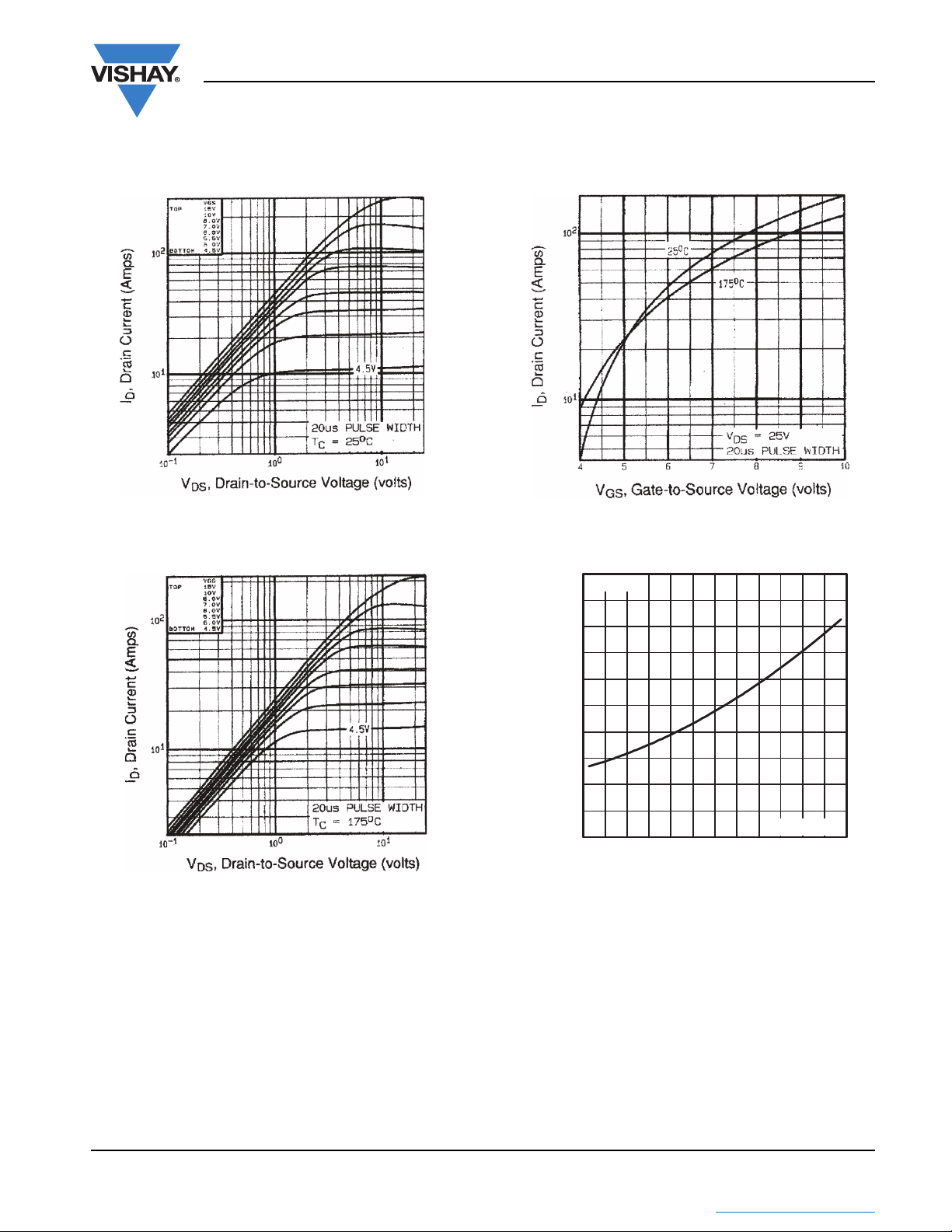
-60 -40 -20 0 20 40 60 80 100 120 140 160 180
0.0
0.5
1.0
1.5
2.0
2.5
T , Junction Temperature ( C)
R , Drain-to-Source On Resistance
(Normalized)
J
DS(on)
°
V =
I =
GS
D
10V
51A
IRFZ44R, SiHFZ44R
TYPICAL CHARACTERISTICS (25 °C, unless otherwise noted)
Fig. 1 - Typical Output Characteristics
Vishay Siliconix
Fig. 3 - Typical Transfer Characteristics
Fig. 2 - Typical Output Characteristics
Document Number: 91292 www.vishay.com
S11-0517-Rev. B, 21-Mar-11 3
THE PRODUCT DESCRIBED HEREIN AND THIS DATASHEET ARE SUBJECT TO SPECIFIC DISCLAIMERS, SET FORTH AT
Fig. 4 - Normalized On-Resistance vs. Temperature
This datasheet is subject to change without notice.
www.vishay.com/doc?91000
 Loading...