

Vishay IRFR420A, IRFU420A, SiHFR420A, SiHFU420A Data Sheet
www.vishay.com
N-Channel MOSFET
G
D
S
IRFR420A, IRFU420A, SiHFR420A, SiHFU420A
Vishay Siliconix
Power MOSFET
PRODUCT SUMMARY
VDS (V) 500
R
()V
DS(on)
Q
max. (nC) 17
g
Q
(nC) 4.3
gs
Q
(nC) 8.5
gd
Configuration Single
= 10 V 3.0
GS
FEATURES
• Low gate Charge Qg results in simple drive
requirement
• Improved gate, avalanche and dynamic dV/dt
ruggedness
• Fully characterized capacitance and
avalanche voltage and current
• Effective C
specified
oss
• Material categorization: for definitions of compliance
DPAK
(TO-252)
D
IPAK
(TO-251)
D
S
G
S
D
G
please see www.vishay.com/doc?99912
APPLICATIONS
• Switch mode power supply (SMPS)
• Uninterruptible power supply
• High speed power switching
ORDERING INFORMATION
Package DPAK (TO-252) DPAK (TO-252) DPAK (TO-252) IPAK (TO-251)
Lead (Pb)-free and Halogen-free SiHFR420A-GE3 SiHFR420ATR-GE3
Lead (Pb)-free IRFR420APbF IRFR420ATRPbF
Note
a. See device orientation.
a
SiHFR420ATRL-GE3 SiHFU420A-GE3
a
IRFR420ATRLPbF IRFU420APbF
Available
ABSOLUTE MAXIMUM RATINGS (TC = 25 °C, unless otherwise noted)
PARAMETER SYMBOL LIMIT UNIT
Drain-Source Voltage V
Gate-Source Voltage V
T
= 25 °C
Continuous Drain Current V
Pulsed Drain Current
a
at 10 V
GS
C
= 100 °C 2.1
C
DS
± 30
GS
I
D
IDM 10
Linear Derating Factor 0.67 W/°C
Single Pulse Avalanche Energy
Repetitive Avalanche Current
Repetitive Avalanche Energy
Maximum Power Dissipation T
Peak Diode Recovery dV/dt
Operating Junction and Storage Temperature Range T
Soldering Recommendations (Peak temperature)
b
a
a
= 25 °C P
c
d
C
for 10 s 300
E
AS
I
AR
E
AR
D
dV/dt 3.4 V/ns
, T
J
stg
Notes
a. Repetitive rating; pulse width limited by maximum junction temperature (see fig. 11).
b. Starting T
c. I
SD
= 25 °C, L = 45 mH, Rg = 25 , IAS = 2.5 A (see fig. 12).
J
2.5 A, dI/dt 270 A/μs, VDD VDS, TJ 150 °C.
d. 1.6 mm from case.
S16-1522-Rev. D, 08-Aug-16
1
For technical questions, contact: hvm@vishay.com
THIS DOCUMENT IS SUBJECT TO CHANGE WITHOUT NOTICE. THE PRODUCTS DESCRIBED HEREIN AND THIS DOCUMENT
ARE SUBJECT TO SPECIFIC DISCLAIMERS, SET FORTH AT www.vishay.com/doc?91000
500
3.3
140 mJ
2.5 A
5.0 mJ
83 W
-55 to +150
Document Number: 91274
V
AT
°C
IRFR420A, IRFU420A, SiHFR420A, SiHFU420A
S
D
G
www.vishay.com
THERMAL RESISTANCE RATINGS
PARAMETER SYMBOL TYP. MAX. UNIT
Maximum Junction-to-Ambient R
Maximum Junction-to-Case (Drain) R
thJA
thCS
thJC
-62
0.50 -
-1.5
SPECIFICATIONS (TJ = 25 °C, unless otherwise noted)
PARAMETER SYMBOL TEST CONDITIONS MIN. TYP. MAX. UNIT
Static
Drain-Source Breakdown Voltage V
V
Temperature Coefficient VDS/TJ Reference to 25 °C, ID = 1 mA - 0.60 - V/°C
DS
Gate-Source Threshold Voltage V
Gate-Source Leakage I
Zero Gate Voltage Drain Current I
Drain-Source On-State Resistance R
Forward Transconductance g
DS
GS(th)
V
GSS
DSS
VGS = 10 V ID = 1.5 A
DS(on)
fs
Dynamic
Input Capacitance C
Reverse Transfer Capacitance C
Output Capacitance C
Effective Output Capacitance C
Total Gate Charge Q
Gate-Drain Charge Q
Turn-On Delay Time t
Rise Time t
Turn-Off Delay Time t
Fall Time t
iss
-53-
oss
-2.7-
rss
oss
eff. VDS = 0 V to 400 V
oss
g
--4.3
gs
--8.5
gd
d(on)
r
-16-
d(off)
-13-
f
Drain-Source Body Diode Characteristics
Continuous Source-Drain Diode Current I
Pulsed Diode Forward Current
a
Body Diode Voltage V
Body Diode Reverse Recovery Time t
Body Diode Reverse Recovery Charge Q
Forward Turn-On Time t
S
I
SM
SD
rr
rr
on
MOSFET symbol
showing the
integral reverse
p - n junction diode
TJ = 25 °C, IF = 2.5 A, dI/dt = 100 A/μs
Notes
a. Repetitive rating; pulse width limited by maximum junction temperature (see fig. 11).
b. Pulse width 300 μs; duty cycle 2 %.
c. C
eff. is a fixed capacitance that gives the same charging time as C
oss
VGS = 0 V, ID = 250 μA 500 - - V
VDS = VGS, ID = 250 μA 2.0 - 4.5 V
= ± 30 V - - ± 100 nA
GS
VDS = 500 V, VGS = 0 V - - 25
= 400 V, VGS = 0 V, TJ = 125 °C - - 250
V
DS
b
VDS = 50 V, ID = 1.5 A 1.4 - - S
VGS = 0 V,
V
= 25 V,
DS
f = 1.0 MHz, see fig. 5
= 1.0 V, f = 1.0 MHz - 490 -
V
DS
= 0 V
V
GS
V
= 10 V
GS
V
DD
R
= 21 , RD = 97 , see fig. 10
g
TJ = 25 °C, IS = 2.5 A, VGS = 0 V
= 400 V, f = 1.0 MHz - 15 -
DS
= 2.5 A, VDS = 400 V,
I
D
see fig. 6 and 13
= 250 V, ID = 2.5 A,
c
b
b
b
b
Intrinsic turn-on time is negligible (turn-on is dominated by LS and LD)
while VDS is rising from 0 % to 80 % VDS.
oss
Vishay Siliconix
°C/WCase-to-Sink, Flat, Greased Surface R
--3.0
- 340 -
-28-
--17
-8.1-
-12-
--3.3
--10
--1.6V
- 330 500 ns
- 760 1140 μC
μA
pFOutput Capacitance C
pFV
nC Gate-Source Charge Q
ns
A
S16-1522-Rev. D, 08-Aug-16
THIS DOCUMENT IS SUBJECT TO CHANGE WITHOUT NOTICE. THE PRODUCTS DESCRIBED HEREIN AND THIS DOCUMENT
ARE SUBJECT TO SPECIFIC DISCLAIMERS, SET FORTH AT www.vishay.com/doc?91000
For technical questions, contact: hvm@vishay.com
2
Document Number: 91274
IRFR420A, IRFU420A, SiHFR420A, SiHFU420A
www.vishay.com
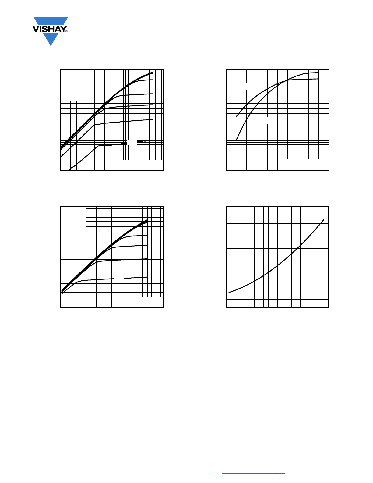
TYPICAL CHARACTERISTICS (25 °C, unless otherwise noted)
Vishay Siliconix
10
1
0.1
TOP
BOTTOM
VGS
15V
10V
8.0V
7.0V
6.0V
5.5V
5.0V
4.5V
4.5V
D
I , Drain-to-Source Current (A)
20μs PULSE WIDTH
°
T = 25 C
0.01
0.1 1 10 100
V , Drain-to-Source Voltage (V)
DS
J
Fig. 1 - Typical Output Characteristics
10
TOP
BOTTOM
VGS
15V
10V
8.0V
7.0V
6.0V
5.5V
5.0V
4.5V
10
°
T = 150 C
J
1
°
T = 25 C
J
0.1
D
I , Drain-to-Source Current (A)
V = 50V
DS
0.01
4.0 5.0 6.0 7.0 8.0 9.0
V , Gate-to-Source Voltage (V)
GS
20μs PULSE WIDTH
Fig. 3 - Typical Transfer Characteristics
3.0
2.5
2.0
I =
D
2.5A
1
4.5V
D
I , Drain-to-Source Current (A)
20μs PULSE WIDTH
0.1
1 10 100
V , Drain-to-Source Voltage (V)
DS
T = 150 C
°
J
Fig. 2 - Typical Output Characteristics
1.5
(Normalized)
1.0
0.5
DS(on)
R , Drain-to-Source On Resistance
0.0
-60 -40 -20 0 20 40 60 80 100 120 140 160
T , Junction Temperature ( C)
J
V =
GS
°
10V
Fig. 4 - Normalized On-Resistance vs. Temperature
S16-1522-Rev. D, 08-Aug-16
3
Document Number: 91274
For technical questions, contact: hvm@vishay.com
THIS DOCUMENT IS SUBJECT TO CHANGE WITHOUT NOTICE. THE PRODUCTS DESCRIBED HEREIN AND THIS DOCUMENT
ARE SUBJECT TO SPECIFIC DISCLAIMERS, SET FORTH AT www.vishay.com/doc?91000
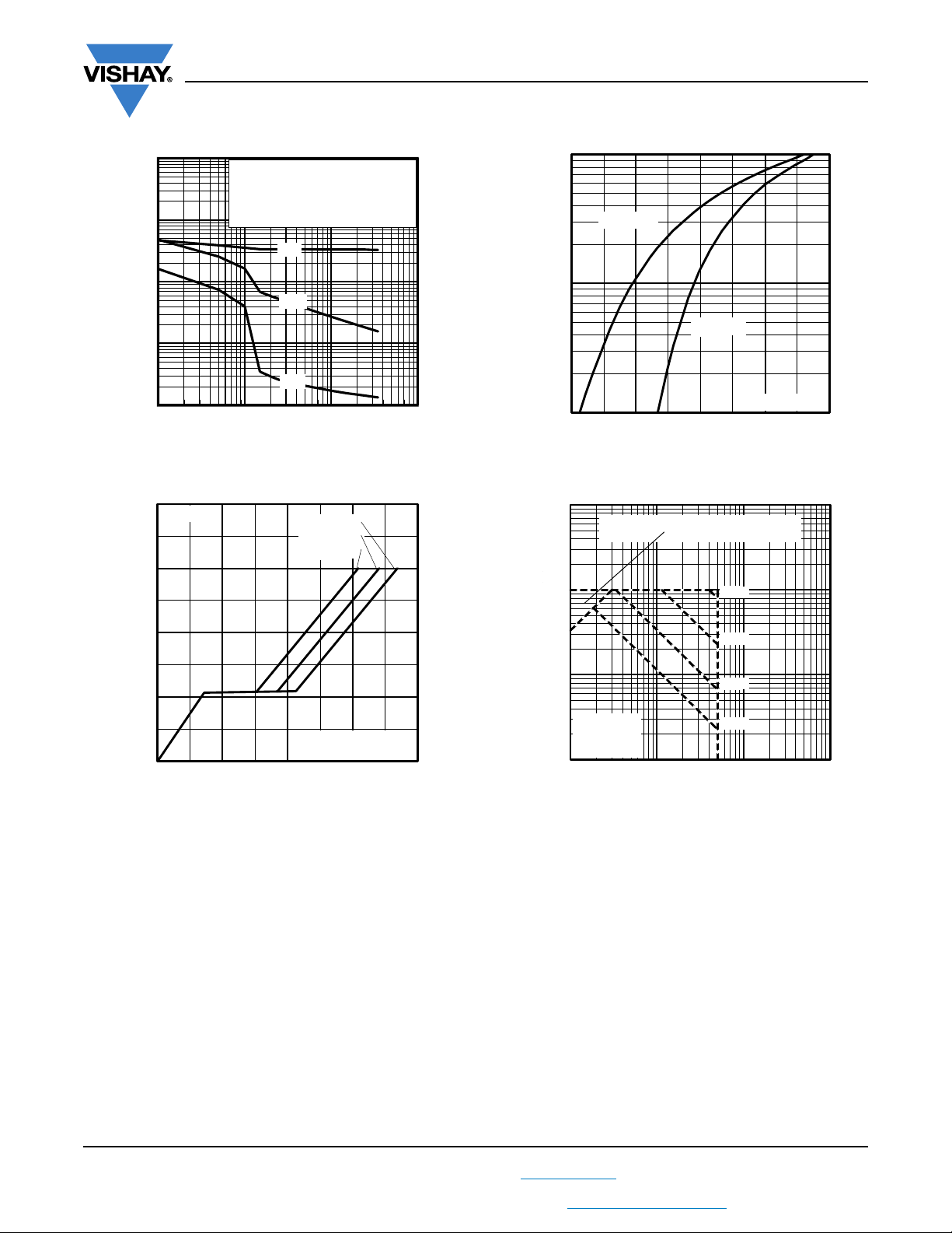
www.vishay.com
IRFR420A, IRFU420A, SiHFR420A, SiHFU420A
Vishay Siliconix
10 000
1000
)
F
p
(
e
c
n
a
t
i
100
c
a
p
a
C
,
C
10
1
1 10 100 1000
V
= 0V, f = 1 MHz
GS
C
= C
iss
gs
C
= C
rss
gd
C
= C
C
ds
C
C
+ C
iss
oss
rss
oss
+ Cgd, C
gd
ds
shorted
VDS, Drain-to-Source Voltage (V)
Fig. 5 - Typical Capacitance vs. Drain-to-Source Voltage
20
I =
2.5A
D
15
V = 400V
DS
V = 250V
DS
V = 100V
DS
10
°
T = 150 C
J
1
°
T = 25 C
J
SD
I , Reverse Drain Current (A)
V = 0 V
0.1
0.4 0.6 0.8 1.0 1.2
V ,Source-to-Drain Voltage (V)
SD
GS
Fig. 7 - Typical Source-Drain Diode Forward Voltage
100
OPERATION IN THIS AREA LIMITED
10
BY R
DS(on)
10us
10
5
GS
V , Gate-to-Source Voltage (V)
FOR TEST CIRCUIT
0
0 4 8 12 16
Q , Total Gate Charge (nC)
G
SEE FIGURE
13
Fig. 6 - Typical Gate Charge vs. Gate-to-Source Voltage
100us
1
D
I , Drain Current (A)I , Drain Current (A)
°
= 25 C
C
T T= 150 C
Single Pulse
0.1
10 100 1000 10000
°
J
V , Drain-to-Source Voltage (V)
DS
1ms
10ms
Fig. 8 - Maximum Safe Operating Area
S16-1522-Rev. D, 08-Aug-16
4
Document Number: 91274
For technical questions, contact: hvm@vishay.com
THIS DOCUMENT IS SUBJECT TO CHANGE WITHOUT NOTICE. THE PRODUCTS DESCRIBED HEREIN AND THIS DOCUMENT
ARE SUBJECT TO SPECIFIC DISCLAIMERS, SET FORTH AT www.vishay.com/doc?91000
 Loading...