

Vishay IRFR224, IRFU224, SiHFR224, SiHFU224 Data Sheet
www.vishay.com
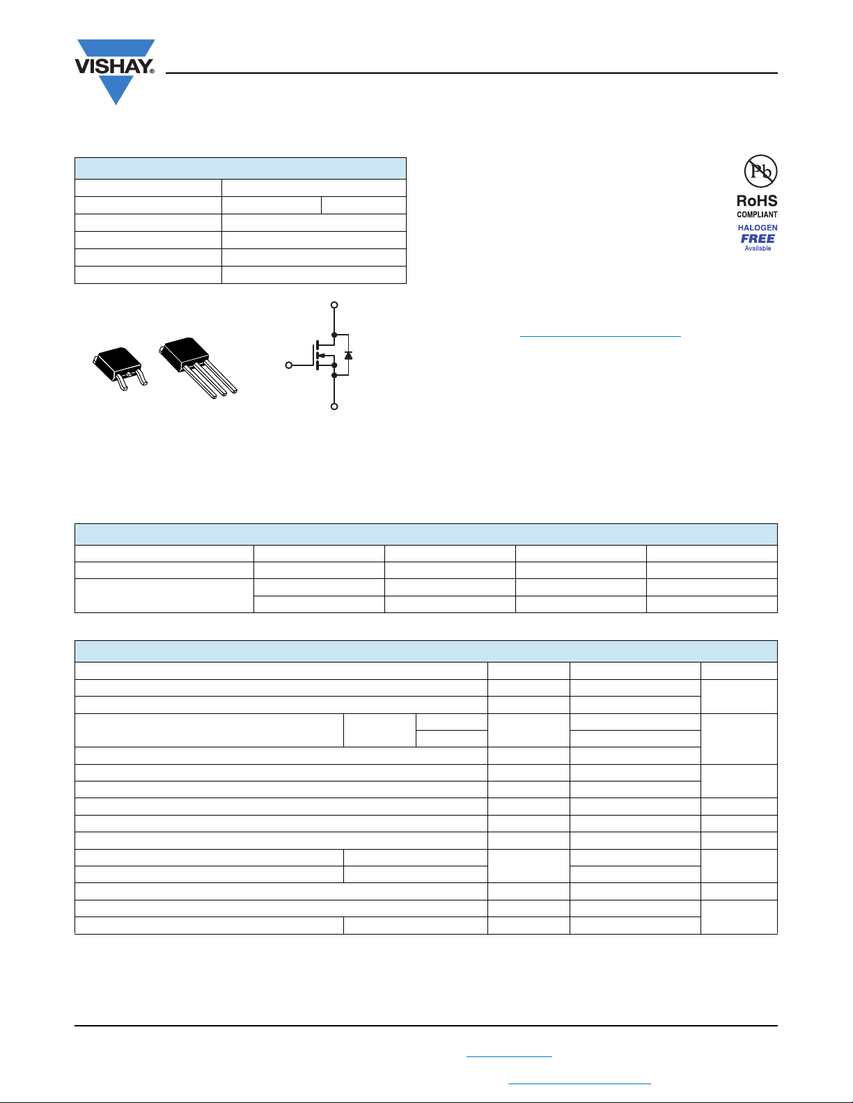
DPAK
(TO-252)
IPAK
(TO-251)
G
D
S
S
D
G
D
IRFR224, IRFU224, SiHFR224, SiHFU224
Vishay Siliconix
Power MOSFET
PRODUCT SUMMARY
VDS (V) 250
R
()V
DS(on)
Q
(Max.) (nC) 14
g
Q
(nC) 2.7
gs
Q
(nC) 7.8
gd
= 10 V 1.1
GS
Configuration Single
D
G
S
N-Channel MOSFET
ORDERING INFORMATION
Package DPAK (TO-252) DPAK (TO-252) DPAK (TO-252) IPAK (TO-251)
Lead (Pb)-free and Halogen-free SiHFR224-GE3 SiHFR224TR-GE3 SiHFR224TRL-GE3 SiHFU224-GE3
Lead (Pb)-free
Note
a. See device orientation.
IRFR224PbF IRFR224TRPbF
SiHFR224-E3 SiHFR224T-E3
ABSOLUTE MAXIMUM RATINGS (TC = 25 °C, unless otherwise noted)
PARAMETER SYMBOL LIMIT UNIT
Drain-Source Voltage V
Gate-Source Voltage V
Continuous Drain Current V
Pulsed Drain Current
a
Linear Derating Factor 0.33
Linear Derating Factor (PCB Mount)
Single Pulse Avalanche Energy
Repetitive Avalanche Current
Repetitive Avalanche Energy
e
b
a
a
Maximum Power Dissipation T
Maximum Power Dissipation (PCB Mount)
Peak Diode Recovery dV/dt
c
e
Operating Junction and Storage Temperature Range T
Soldering Recommendations (Peak Temperature)
Notes
a. Repetitive rating; pulse width limited by maximum junction temperature (see fig. 11).
= 50 V; starting TJ = 25 °C, L = 14 mH, Rg = 25 , IAS = 3.8 A (see fig. 12).
b. V
DD
c. I
3.8 A, dI/dt 90 A/μs, VDD VDS, TJ 150 °C.
SD
d. 1.6 mm from case.
e. When mounted on 1" square PCB (FR-4 or G-10 material).
S13-0165-Rev. C, 04-Feb-13
For technical questions, contact: hvm@vishay.com
THIS DOCUMENT IS SUBJECT TO CHANGE WITHOUT NOTICE. THE PRODUCTS DESCRIBED HEREIN AND THIS DOCUMENT
ARE SUBJECT TO SPECIFIC DISCLAIMERS, SET FORTH AT www.vishay.com/doc?91000
at 10 V
GS
= 25 °C
C
TA = 25 °C 2.5
d
for 10 s 260
FEATURES
• Dynamic dV/dt Rating
• Repetitive Avalanche Rated
• Surface Mount (IRFR224, SiHFR224)
• Straight Lead (IRFU224, SiHFU224)
• Available in Tape and Reel
• Fast Switching
• Ease of Paralleling
• Material categorization: For definitions of compliance
please see www.vishay.com/doc?99912
DESCRIPTION
Third generation power MOSFETs form Vishay provide the
designer with the best combination of fast switching,
ruggedized device design, low on-resistance and
cost-effectiveness.
The DPAK is designed for surface mounting using vapor
phase, infrared, or wave solderig techniques. The straight
lead version (IRFU, SiHFU series) is for through-hole
mounting applications. Power dissipation levels up to 1.5 W
are possible in typical surface mount applications.
a
IRFR224TRLPbFa IRFU224PbF
a
T
= 25 °C
C
= 100 °C 2.4
T
C
SiHFR224TL-E3
DS
± 20
GS
I
D
IDM 15
E
AS
I
AR
E
AR
P
D
dV/dt 4.8 V/ns
, T
J
stg
1
a
SiHFU224-E3
250
3.8
0.020
130 mJ
3.8 A
4.2 mJ
42
- 55 to + 150
Document Number: 91271
V
A
W/°C
W
°C
IRFR224, IRFU224, SiHFR224, SiHFU224
D
S
G
S
D
G
www.vishay.com
THERMAL RESISTANCE RATINGS
PARAMETER SYMBOL TYP. MAX. UNIT
Maximum Junction-to-Ambient
(PCB Mount)
a
Maximum Junction-to-Ambient R
Maximum Junction-to-Case R
R
thJA
thJA
thJC
-50
- 110
-3.0
Note
a. When mounted on 1" square PCB ( FR-4 or G-10 material).
SPECIFICATIONS (TJ = 25 °C, unless otherwise noted)
PARAMETER SYMBOL TEST CONDITIONS MIN. TYP. MAX. UNIT
Static
Drain-Source Breakdown Voltage V
V
Temperature Coefficient VDS/TJ Reference to 25 °C, ID = 1 mA - 0.36 - V/°C
DS
Gate-Source Threshold Voltage V
Gate-Source Leakage I
Zero Gate Voltage Drain Current I
Drain-Source On-State Resistance R
Forward Transconductance g
DS
GS(th)
V
GSS
DSS
VGS = 10 V ID = 2.3 A
DS(on)
fs
Dynamic
Input Capacitance C
Reverse Transfer Capacitance C
Total Gate Charge Q
Gate-Drain Charge Q
Turn-On Delay Time t
Rise Time t
Turn-Off Delay Time t
Fall Time t
Internal Drain Inductance L
iss
-77-
oss
-15-
rss
g
--2.7
gs
--7.8
gd
d(on)
r
-20-
d(off)
-12-
f
D
V
Between lead,
6 mm (0.25") from
package and center of
Internal Source Inductance L
S
die contact
VGS = 0 V, ID = 250 μA 250 - - V
VDS = VGS, ID = 250 μA 2.0 - 4.0 V
= ± 20 V - - ± 100 nA
GS
VDS = 250 V, VGS = 0 V - - 25
V
= 200 V, VGS = 0 V, TJ = 125 °C - - 250
DS
b
VDS = 50 V, ID = 2.3 A
b
VGS = 0 V,
V
= 25 V,
f = 1.0 MHz, see fig. 5
= 10 V
GS
V
= 125 V, ID = 4.4 A,
DD
R
= 18 , RD = 28 ,
G
see fig. 10
DS
= 4.4 A, VDS = 200 V,
I
D
see fig. 6 and 13
b, c
c
b, c
Vishay Siliconix
°C/W
--1.1
1.5 - - S
- 260 -
--14
-7.0-
-13-
-4.5-
-7.5-
μA
pFOutput Capacitance C
nC Gate-Source Charge Q
ns
nH
Drain-Source Body Diode Characteristics
Continuous Source-Drain Diode Current I
Pulsed Diode Forward Current
a
Body Diode Voltage V
Body Diode Reverse Recovery Time t
Body Diode Reverse Recovery Charge Q
Forward Turn-On Time t
S
I
SM
SD
rr
rr
on
MOSFET symbol
showing the
integral reverse
p - n junction diode
TJ = 25 °C, IS = 3.8 A, VGS = 0 V
b
TJ = 25 °C, IF = 4.4 A, dI/dt = 100 A/μs
Intrinsic turn-on time is negligible (turn-on is dominated by LS and LD)
--3.8
--15
--1.8V
- 200 400 ns
b
- 0.93 1.9 μC
A
Notes
a. Repetitive rating; pulse width limited by maximum junction temperature (see fig. 11).
b. Pulse width 300 μs; duty cycle 2 %.
THIS DOCUMENT IS SUBJECT TO CHANGE WITHOUT NOTICE. THE PRODUCTS DESCRIBED HEREIN AND THIS DOCUMENT
ARE SUBJECT TO SPECIFIC DISCLAIMERS, SET FORTH AT www.vishay.com/doc?91000
For technical questions, contact: hvm@vishay.com
S13-0165-Rev. C, 04-Feb-13
2
Document Number: 91271
IRFR224, IRFU224, SiHFR224, SiHFU224
www.vishay.com
TYPICAL CHARACTERISTICS (25 °C, unless otherwise noted)
Vishay Siliconix
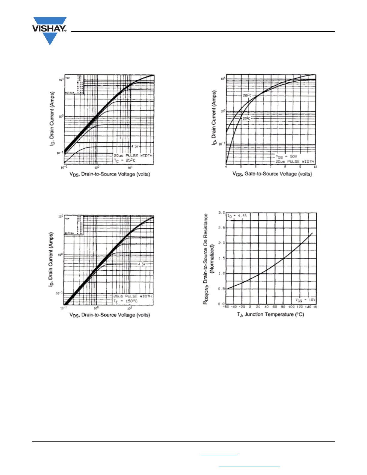
Fig. 1 - Typical Output Characteristics, TC = 25 °C
Fig. 2 - Typical Output Characteristics, T
= 150 °C
C
Fig. 3 - Typical Transfer Characteristics
Fig. 4 - Normalized On-Resistance vs. Temperature
S13-0165-Rev. C, 04-Feb-13
For technical questions, contact: hvm@vishay.com
THIS DOCUMENT IS SUBJECT TO CHANGE WITHOUT NOTICE. THE PRODUCTS DESCRIBED HEREIN AND THIS DOCUMENT
ARE SUBJECT TO SPECIFIC DISCLAIMERS, SET FORTH AT www.vishay.com/doc?91000
3
Document Number: 91271
www.vishay.com
IRFR224, IRFU224, SiHFR224, SiHFU224
Vishay Siliconix
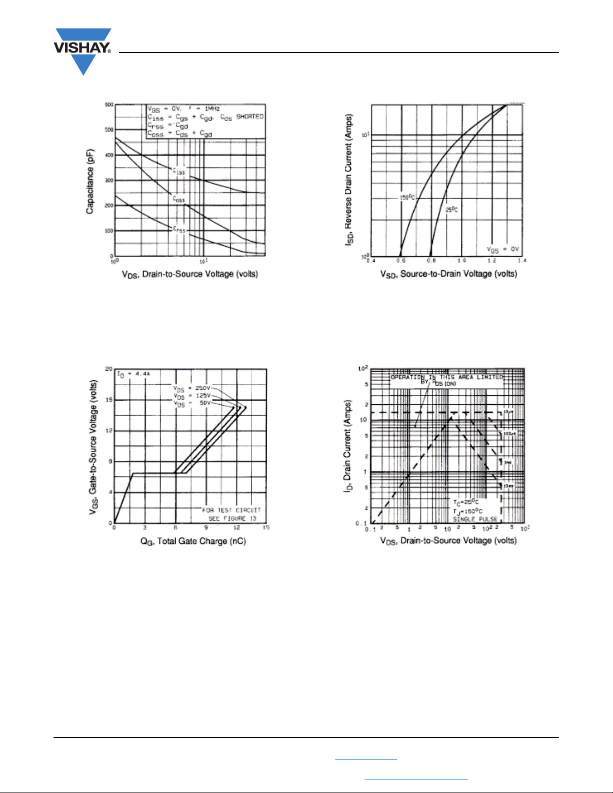
Fig. 5 - Typical Capacitance vs. Drain-to-Source Voltage
Fig. 6 - Typical Gate Charge vs. Gate-to-Source Voltage
Fig. 7 - Typical Source-Drain Diode Forward Voltage
Fig. 8 - Maximum Safe Operating Area
S13-0165-Rev. C, 04-Feb-13
For technical questions, contact: hvm@vishay.com
THIS DOCUMENT IS SUBJECT TO CHANGE WITHOUT NOTICE. THE PRODUCTS DESCRIBED HEREIN AND THIS DOCUMENT
ARE SUBJECT TO SPECIFIC DISCLAIMERS, SET FORTH AT www.vishay.com/doc?91000
4
Document Number: 91271
 Loading...