

IRFPS37N50A, SiHFPS37N50A
S
D
G
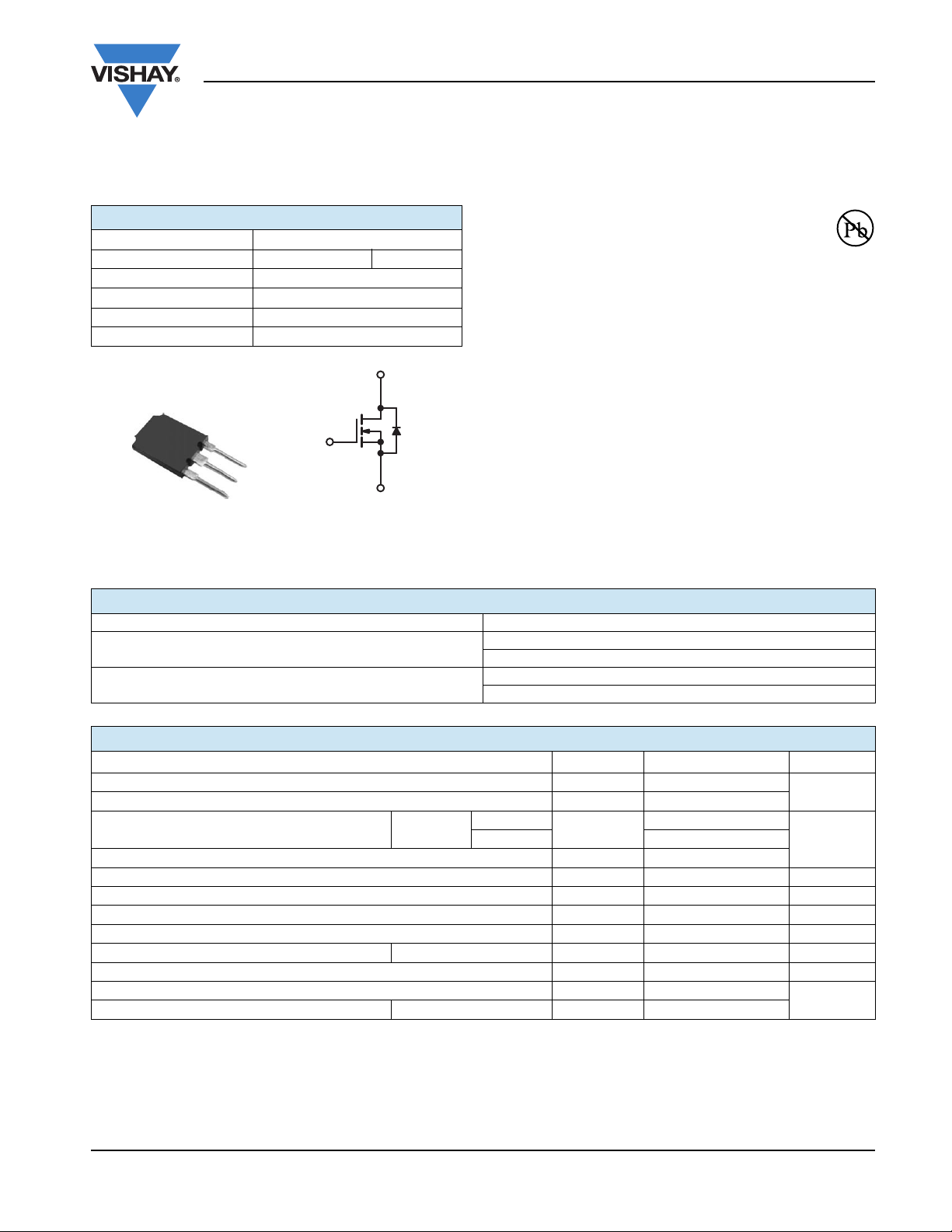
Super-247
Available
RoHS*
COMPLIANT
Power MOSFET
Vishay Siliconix
PRODUCT SUMMARY
VDS (V) 500
R
(Max.) ()V
DS(on)
Q
(Max.) (nC) 180
g
Q
(nC) 46
gs
Q
(nC) 71
gd
= 10 V 0.13
GS
Configuration Single
G
N-Channel MOSFET
ORDERING INFORMATION
Package
Lead (Pb)-free
SnPb
FEATURES
• Low Gate Charge Qg Results in Simple Drive
Requirement
• Improved Gate, Avalanche and Dynamic dV/dt
Ruggedness
• Fully Characterized Capacitance and Avalanche Voltage
and Current
D
• Effective C
Specified
oss
• Compliant to RoHS Directive 2002/95/EC
APPLICATIONS
• Switch Mode Power Supply (SMPS)
• Uninterruptible Power Supply
• High Speed Power Switching
S
TYPICAL SMPS TOPOLOGIES
• Full Bridge Converters
• Power Factor Correction Boost
Super-247
IRFPS37N50APbF
SiHFPS37N50A-E3
IRFPS37N50A
SiHFPS37N50A
ABSOLUTE MAXIMUM RATINGS (TC = 25 °C, unless otherwise noted)
PARAMETER SYMBOL LIMIT UNIT
Drain-Source Voltage V
Gate-Source Voltage V
= 25 °C
T
Continuous Drain Current V
Pulsed Drain Current
a
at 10 V
GS
C
= 100 °C 23
T
C
DS
± 30
GS
I
D
IDM 144
Linear Derating Factor 3.6 W/°C
Single Pulse Avalanche Energy
Repetitive Avalanche Current
Repetitive Avalanche Energy
Maximum Power Dissipation T
Peak Diode Recovery dV/dt
Operating Junction and Storage Temperature Range T
b
a
a
= 25 °C P
c
C
E
AS
I
AR
E
AR
D
dV/dt 3.5 V/ns
, T
J
stg
Soldering Recommendations (Peak Temperature) for 10 s 300
Notes
a. Repetitive rating; pulse width limited by maximum junction temperature (see fig. 11).
b. Starting T
c. I
SD
= 25 °C, L = 1.94 mH, Rg = 25 , IAS = 36 A (see fig. 12).
J
36 A, dI/dt 145 A/μs, VDD VDS, TJ 150 °C.
d. 1.6 mm from case.
* Pb containing terminations are not RoHS compliant, exemptions may apply
Document Number: 91258 www.vishay.com
S11-0111-Rev. C, 07-Feb-11 1
500
36
1260 mJ
36 A
44 mJ
446 W
- 55 to + 150
d
V
A
°C
IRFPS37N50A, SiHFPS37N50A
Vishay Siliconix
THERMAL RESISTANCE RATINGS
PARAMETER SYMBOL TYP. MAX. UNIT
Maximum Junction-to-Ambient R
Maximum Junction-to-Case (Drain) R
thJA
thCS
thJC
SPECIFICATIONS (TJ = 25 °C, unless otherwise noted)
PARAMETER SYMBOL TEST CONDITIONS MIN. TYP. MAX. UNIT
Static
Drain-Source Breakdown Voltage V
Gate-Source Threshold Voltage V
Gate-Source Leakage I
Zero Gate Voltage Drain Current I
Drain-Source On-State Resistance R
Forward Transconductance g
Dynamic
Input Capacitance C
Output Capacitance C
Reverse Transfer Capacitance C
Output Capacitance C
Effective Output Capacitance C
Total Gate Charge Q
Gate-Drain Charge Q
Turn-On Delay Time t
Rise Time t
Turn-Off Delay Time t
Fall Time t
Drain-Source Body Diode Characteristics
Continuous Source-Drain Diode Current I
Pulsed Diode Forward Current
a
Body Diode Voltage V
Body Diode Reverse Recovery Time t
Body Diode Reverse Recovery Charge Q
Forward Turn-On Time t
Notes
a. Repetitive rating; pulse width limited by maximum junction temperature (see fig. 11).
b. Pulse width 300 μs; duty cycle 2 %.
c. C
eff. is a fixed capacitance that gives the same charging time as C
oss
DS
GS(th)
V
GSS
DSS
VGS = 10 V ID = 22 A
DS(on)
fs
iss
- 810 -
oss
-36-
rss
oss
eff. VDS = 0 V to 400 V - 400 -
oss
g
--46
gs
--71
gd
d(on)
r
-52-
d(off)
-80-
f
S
I
SM
SD
rr
rr
on
V
V
GS
V
GS
MOSFET symbol
showing the
integral reverse
p - n junction diode
TJ = 25 °C, IF = 36 A, dI/dt = 100 A/μs
-40
0.24 -
°C/WCase-to-Sink, Flat, Greased Surface R
-0.28
VGS = 0 V, ID = 250 μA 500 - - V
VDS = VGS, ID = 250 μA 2.0 - 4.0 V
= ± 30 V - - ± 100 nA
GS
VDS = 500 V, VGS = 0 V - - 25
= 400 V, VGS = 0 V, TJ = 150 °C - - 250
DS
VDS = 50 V, ID = 22 A
VGS = 0 V,
V
= 25 V,
DS
f = 1.0 MHz, see fig. 5
= 1.0 V , f = 1.0 MHz - 7905 -
V
DS
= 0 V
V
= 400 V , f = 1.0 MHz - 221 -
DS
b
b
- - 0.13
20 - - S
- 5579 -
- - 180
= 36 A, VDS = 400 V,
I
= 10 V
D
see fig. 6 and 13
b
-23-
V
= 250 V, ID = 36 A,
DD
R
= 2.15 , RD = 7.0
G
see fig. 10
b
G
TJ = 25 °C, IS = 36 A, VGS = 0 V
D
S
b
-98-
--36
- - 144
--1.5V
- 570 860 ns
b
- 8.6 13 μC
Intrinsic turn-on time is negligible (turn-on is dominated by LS and LD)
while VDS is rising from 0 % to 80 % VDS.
oss
μA
pF
nC Gate-Source Charge Q
ns
A
www.vishay.com Document Number: 91258
2 S11-0111-Rev. C, 07-Feb-11
IRFPS37N50A, SiHFPS37N50A
0.1
1
10
100
1000
0.1 1 10 100
20µs PULSE WIDTH
T = 25 C
J
°
TOP
BOTTOM
VGS
15V
10V
8.0V
7.0V
6.0V
5.5V
5.0V
4.5V
V , Drain-to-Source Voltage (V)
I , Drain-to-Source Current (A)
DS
D
4.5V
1
10
100
0.1 1 10 100
20µs PULSE WIDTH
T = 150 C
J
°
TOP
BOTTOM
VGS
15V
10V
8.0V
7.0V
6.0V
5.5V
5.0V
4.5V
V , Drain-to-Source Voltage (V)
I , Drain-to-Source Current (A)
DS
D
4.5V
1
10
100
1000
4.0 5.0 6.0 7.0 8.0 9.0
V = 50V
20µs PULSE WIDT H
DS
V , Gate-to-Source Voltage (V)
I , Drain-to-Source Current (A)
GS
D
T = 25 C
J
°
T = 150 C
J
°
-60 -40 -20 0 20 40 60 80 100 120 140 160
0.0
0.5
1.0
1.5
2.0
2.5
3.0
T , Junction Temperature ( C)
R , Drain-to-Source On Resistance
(Normalized)
J
DS(on)
°
V =
I =
GS
D
10V
36A
TYPICAL CHARACTERISTICS (25 °C, unless otherwise noted)
Vishay Siliconix
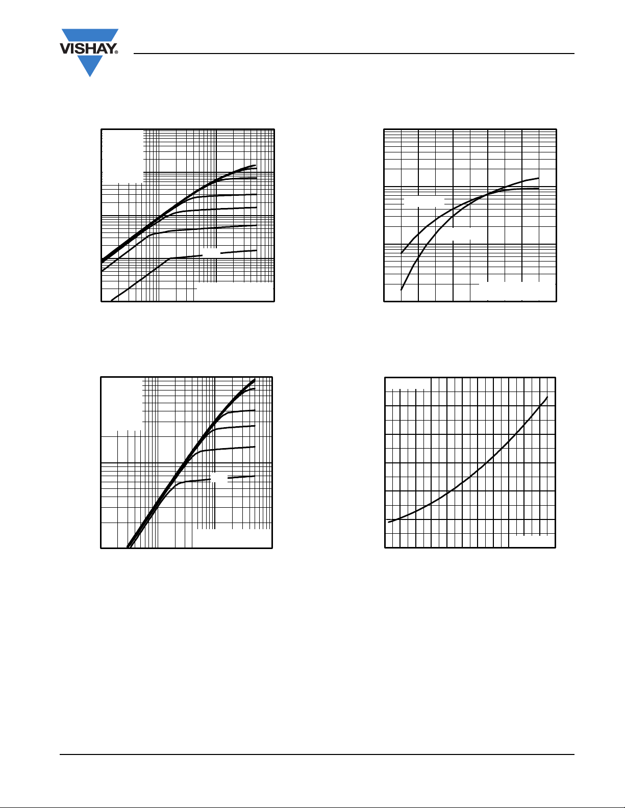
Fig. 1 - Typical Output Characteristics
Fig. 2 - Typical Output Characteristics
Document Number: 91258 www.vishay.com
S11-0111-Rev. C, 07-Feb-11 3
Fig. 3 - Typical Transfer Characteristics
Fig. 4 - Normalized On-Resistance vs. Temperature

IRFPS37N50A, SiHFPS37N50A
10
100
1000
10000
100000
1 10 100 1000
C, Capacitance (pF)
DS
V , Drain-to-Source Voltage (V)
A
V = 0V, f = 1MHz
C = C + C , C SHORTED
C = C
C = C + C
GS
iss gs gd ds
rss gd
oss ds gd
C
iss
C
oss
C
rss
0 40 80 120 160 200
0
4
8
12
16
20
Q , Total Gate Charge (nC)
V , Gate-to-Source Voltage (V)
G
GS
FOR TEST CIRCUIT
SEE FIGURE
I =
D
13
36A
V = 100V
DS
V = 250V
DS
V = 400V
DS
0.1
1
10
100
1000
0.2 0.4 0.6 0.8 1.0 1.2 1.4
V ,Source-to-Drain Voltage (V)
I , Reverse Drain Current (A)
SD
SD
V = 0 V
GS
T = 25 C
J
°
T = 150 C
J
°
1
10
100
1000
10 100 1000 10000
OPERATION IN THIS AREA LIMITED
BY R
DS(on)
Single Pulse
T T= 150 C
= 25 C
°
°
J
C
V , Drain-to-Source Voltage (V)
I , Drain Current (A)I , Drain Current (A)
DS
D
10us
100us
1ms
10ms
Vishay Siliconix
Fig. 5 - Typical Capacitance vs. Drain-to-Source Voltage
Fig. 6 - Typical Gate Charge vs. Gate-to-Source Voltage
www.vishay.com Document Number: 91258
4 S11-0111-Rev. C, 07-Feb-11
Fig. 7 - Typical Source-Drain Diode Forward Voltage
Fig. 8 - Maximum Safe Operating Area

IRFPS37N50A, SiHFPS37N50A
25 50 75 100 125 150
0
10
20
30
40
T , Case Temperature ( C)
I , Drain Current (A)
°
C
D
V
DS
90 %
10 %
V
GS
t
d(on)
t
r
t
d(off)
t
f
0.001
0.01
0.1
1
0.00001 0.0001 0.001 0.01 0.1 1
Notes:
1. Duty factor D = t / t
2. Peak T =P x Z + T
1 2
J DM thJC C
P
t
t
DM
1
2
t , Rectangular Pulse Duration (sec)
Thermal Response
(Z )
1
thJC
0.01
0.02
0.05
0.10
0.20
D = 0.50
SINGLE PULSE
(THERMAL RESPONSE)
Vishay Siliconix
R
D.U.T.
D
+
V
-
DD
V
DS
V
GS
R
G
10 V
Pulse width ≤ 1 µs
Duty factor ≤ 0.1 %
Fig. 10a - Switching Time Test Circuit
Fig. 9 - Maximum Drain Current vs. Case Temperature
Fig. 11 - Maximum Effective Transient Thermal Impedance, Junction-to-Case
Fig. 10b - Switching Time Waveforms
Document Number: 91258 www.vishay.com
S11-0111-Rev. C, 07-Feb-11 5

IRFPS37N50A, SiHFPS37N50A
A
R
G
I
AS
0.01 Ω
t
p
D.U.T.
L
V
DS
+
-
V
DD
Driver
15 V
20 V
I
AS
V
DS
t
p
25 50 75 100 125 150
0
500
1000
1500
2000
2500
3000
Starting T , Junction Temperature ( C)
E , Single Pulse Avalanche Energy (mJ)
J
AS
°
I
D
TOP
BOTTOM
16A
23A
36A
A
D.U.T.
3 mA
V
GS
V
DS
I
G
I
D
0.3 µF
0.2 µF
50 kΩ
12 V
Current regulator
Current sampling resistors
Same type as D.U.T.
+
-
Vishay Siliconix
Fig. 12a - Unclamped Inductive Test Circuit
580
560
540
520
DSav
V , Avalanche Voltage (V)
500
010203040
I , Avalanche Current (A)
av
Fig. 12d - Maximum Avalanche Energy vs. Drain Current
Q
10 V
G
Fig. 12b - Unclamped Inductive Waveforms
Q
GS
V
G
Q
GD
Charge
Fig. 13a - Basic Gate Charge Waveform
Fig. 12c - Maximum Avalanche Energy vs. Drain Current
Fig. 13b - Gate Charge Test Circuit
www.vishay.com Document Number: 91258
6 S11-0111-Rev. C, 07-Feb-11

P.W.
Period
dI/dt
Diode recovery
dV/dt
Ripple ≤ 5 %
Body diode forward drop
Re-applied
voltage
Reverse
recovery
current
Body diode forward
current
V
GS
= 10 Va
I
SD
Driver gate drive
D.U.T. l
SD
waveform
D.U.T. V
DS
waveform
Inductor current
D =
P.W.
Period
+
-
+
+
+
-
-
-
Peak Diode Recovery dV/dt Test Circuit
V
DD
• dV/dt controlled by R
g
• Driver same type as D.U.T.
•
I
SD
controlled by duty factor “D”
• D.U.T. - device under test
D.U.T.
Circuit layout considerations
• Low stray inductance
• Ground plane
• Low leakage inductance
current transformer
R
g
Note
a. V
GS
= 5 V for logic level devices
V
DD
IRFPS37N50A, SiHFPS37N50A
Vishay Siliconix
Vishay Siliconix maintains worldwide manufacturing capability. Products may be manufactured at one of several qualified locations. Reliability data for Silicon
Technology and Package Reliability represent a composite of all qualified locations. For related documents such as package/tape drawings, part marking, and
reliability data, see www.vishay.com/ppg?91258
.
Fig. 14 - For N-Channel
Document Number: 91258 www.vishay.com
S11-0111-Rev. C, 07-Feb-11 7

TO-274AA (HIGH VOLTAGE)
B
E4
E
R
Package Information
Vishay Siliconix
A
A
A1
E1
D2
D
L1
L
e
10°
5°
Detail “A”
b
0.10 (0.25)
Lead Tip
MM
B A
C
A2
b2
Detail “A”
Scale: 2:1
b4
D1
MILLIMETERS INCHES MILLIMETERS INCHES
DIM. MIN. MAX. MIN. MAX. DIM. MIN. MAX. MIN. MAX.
A 4.70 5.30 0.185 0.209 D1 15.50 16.10 0.610 0.634
A1 1.50 2.50 0.059 0.098 D2 0.70 1.30 0.028 0.051
A2 2.25 2.65 0.089 0.104 E 15.10 16.10 0.594 0.634
b 1.30 1.60 0.051 0.063 E1 13.30 13.90 0.524 0.547
b2 1.80 2.20 0.071 0.087 e 5.45 BSC 0.215 BSC
b4 3.00 3.25 0.118 0.128 L 13.70 14.70 0.539 0.579
c 0.80 1.20 0.031 0.047 L1 1.00 1.60 0.039 0.063
D 19.80 20.80 0.780 0.819 R 2.00 3.00 0.079 0.118
ECN: S-82247-Rev. A, 06-Oct-08
DWG: 5975
Notes
1. Dimensioning and tolerancing per ASME Y14.5M-1994.
2. Dimension D and E do not include mold flash. Mold flash shall not exceed 0.127 mm (0.005") per side. These dimensions are measured at the
outer extremes of the plastic body.
3. Outline conforms to JEDEC outline to TO-274AA.
Document Number: 91365 www.vishay.com
Revision: 06-Oct-08 1

Legal Disclaimer Notice
www.vishay.com
Vishay
Disclaimer
ALL PRODUCT, PRODUCT SPECIFICATIONS AND DATA ARE SUBJECT TO CHANGE WITHOUT NOTICE TO IMPROVE
RELIABILITY, FUNCTION OR DESIGN OR OTHERWISE.
Vishay Intertechnology, Inc., its affiliates, agents, and employees, and all persons acting on its or their behalf (collectively,
“Vishay”), disclaim any and all liability for any errors, inaccuracies or incompleteness contained in any datasheet or in any other
disclosure relating to any product.
Vishay makes no warranty, representation or guarantee regarding the suitability of the products for any particular purpose or
the continuing production of any product. To the maximum extent permitted by applicable law, Vishay disclaims (i) any and all
liability arising out of the application or use of any product, (ii) any and all liability, including without limitation special,
consequential or incidental damages, and (iii) any and all implied warranties, including warranties of fitness for particular
purpose, non-infringement and merchantability.
Statements regarding the suitability of products for certain types of applications are based on Vishay’s knowledge of typical
requirements that are often placed on Vishay products in generic applications. Such statements are not binding statements
about the suitability of products for a particular application. It is the customer’s responsibility to validate that a particular
product with the properties described in the product specification is suitable for use in a particular application. Parameters
provided in datasheets and/or specifications may vary in different applications and performance may vary over time. All
operating parameters, including typical parameters, must be validated for each customer application by the customer’s
technical experts. Product specifications do not expand or otherwise modify Vishay’s terms and conditions of purchase,
including but not limited to the warranty expressed therein.
Except as expressly indicated in writing, Vishay products are not designed for use in medical, life-saving, or life-sustaining
applications or for any other application in which the failure of the Vishay product could result in personal injury or death.
Customers using or selling Vishay products not expressly indicated for use in such applications do so at their own risk. Please
contact authorized Vishay personnel to obtain written terms and conditions regarding products designed for such applications.
No license, express or implied, by estoppel or otherwise, to any intellectual property rights is granted by this document or by
any conduct of Vishay. Product names and markings noted herein may be trademarks of their respective owners.
Material Category Policy
Vishay Intertechnology, Inc. hereby certifies that all its products that are identified as RoHS-Compliant fulfill the
definitions and restrictions defined under Directive 2011/65/EU of The European Parliament and of the Council
of June 8, 2011 on the restriction of the use of certain hazardous substances in electrical and electronic equipment
(EEE) - recast, unless otherwise specified as non-compliant.
Please note that some Vishay documentation may still make reference to RoHS Directive 2002/95/EC. We confirm that
all the products identified as being compliant to Directive 2002/95/EC conform to Directive 2011/65/EU.
Vishay Intertechnology, Inc. hereby certifies that all its products that are identified as Halogen-Free follow Halogen-Free
requirements as per JEDEC JS709A standards. Please note that some Vishay documentation may still make reference
to the IEC 61249-2-21 definition. We confirm that all the products identified as being compliant to IEC 61249-2-21
conform to JEDEC JS709A standards.
Revision: 02-Oct-12
1
Document Number: 91000
 Loading...