

Vishay IRFP9240, SiHFP9240 Data Sheet
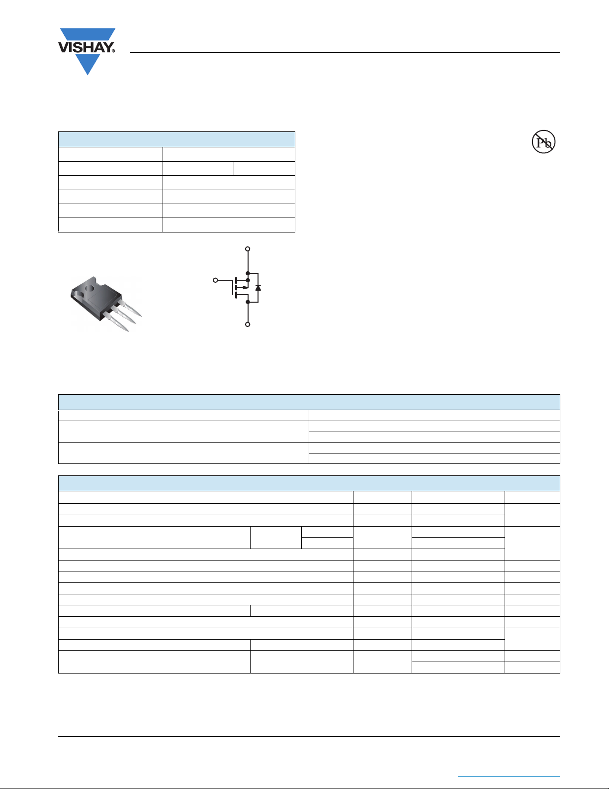
Power MOSFET
S
G
D
P-Channel MOSFET
TO-247AC
G
D
S
Available
RoHS*
COMPLIANT
IRFP9240, SiHFP9240
Vishay Siliconix
PRODUCT SUMMARY
VDS (V) - 200 V
(Max.) (Ω)V
R
DS(on)
Q
(Max.) (nC) 44
g
Q
(nC) 7.1
gs
Q
(nC) 27
gd
Configuration Single
= - 10 V 0.50
GS
FEATURES
• Dynamic dV/dt Rating
• Repetitive Avalanche Rated
• P-Channel
• Isolated Central Mounting Hole
•Fast Switching
• Ease of Paralleling
• Simple Drive Requirements
• Compliant to RoHS Directive 2002/95/EC
DESCRIPTION
Third generation Power MOSFETs from Vishay provide the
designer with the best combination of fast switching,
ruggedized device design, low on-resistance and
cost-effectiveness.
The TO-247AC package is preferred for
commercial-industrial applications where higher power
levels preclude the use of TO-220AB devices. The
TO-247AC is similar but superior to the earlier TO-218
package because of its isolated mounting hole. It also
provides greater creepage distance between pins to meet
the requirements of most safety specifications.
ORDERING INFORMATION
Package TO-247AC
Lead (Pb)-free
SnPb
IRFP9240PbF
SiHFP9240-E3
IRFP9240
SiHFP9240
ABSOLUTE MAXIMUM RATINGS (TC = 25 °C, unless otherwise noted)
PARAMETER SYMBOL LIMIT UNIT
Drain-Source Voltage V
Gate-Source Voltage V
T
= 25 °C
Continuous Drain Current V
Pulsed Drain Current
a
at - 10 V
GS
C
= 100 °C - 7.5
T
C
DS
± 20
GS
I
D
IDM - 48
Linear Derating Factor 1.2 W/°C
Single Pulse Avalanche Energy
Repetitive Avalanche Current
Repetitive Avalanche Energy
Maximum Power Dissipation T
Peak Diode Recovery dV/dt
b
a
a
= 25 °C P
c
C
Operating Junction and Storage Temperature Range T
E
AS
I
AR
E
AR
D
dV/dt - 5.0 V/ns
, T
J
stg
Soldering Recommendations (Peak Temperature) for 10 s 300
Mounting Torque 6-32 or M3 screw
Notes
a. Repetitive rating; pulse width limited by maximum junction temperature (see fig. 11).
b. V
= - 50 V, starting TJ = 25 °C, L = 8.2 mH, Rg = 25 Ω, IAS = - 12 A (see fig. 12).
DD
c. ISD ≤ - 12 A, dI/dt ≤ 150 A/μs, VDD ≤ VDS, TJ ≤ 150 °C.
d. 1.6 mm from case.
* Pb containing terminations are not RoHS compliant, exemptions may apply
Document Number: 91239 www.vishay.com
S11-0444-Rev. B, 14-Mar-11 1
THE PRODUCT DESCRIBED HEREIN AND THIS DATASHEET ARE SUBJECT TO SPECIFIC DISCLAIMERS, SET FORTH AT
This datasheet is subject to change without notice.
- 200
- 12
790 mJ
- 12 A
15 mJ
150 W
- 55 to + 150
d
10 lbf · in
1.1 N · m
www.vishay.com/doc?91000
V
A
°C
IRFP9240, SiHFP9240
Vishay Siliconix
THERMAL RESISTANCE RATINGS
PARAMETER SYMBOL TYP. MAX. UNIT
Maximum Junction-to-Ambient R
Maximum Junction-to-Case (Drain) R
thJA
thCS
thJC
SPECIFICATIONS (TJ = 25 °C, unless otherwise noted)
PARAMETER SYMBOL TEST CONDITIONS MIN. TYP. MAX. UNIT
Static
Drain-Source Breakdown Voltage V
V
Temperature Coefficient ΔVDS/TJ Reference to 25 °C, ID = - 1 mA - - 0.20 - V/°C
DS
Gate-Source Threshold Voltage V
Gate-Source Leakage I
Zero Gate Voltage Drain Current I
Drain-Source On-State Resistance R
Forward Transconductance g
Dynamic
Input Capacitance C
Reverse Transfer Capacitance C
Total Gate Charge Q
Gate-Drain Charge Q
Turn-On Delay Time t
Rise Time t
Turn-Off Delay Time t
Fall Time t
Internal Drain Inductance L
Internal Source Inductance L
Drain-Source Body Diode Characteristics
Continuous Source-Drain Diode Current I
Pulsed Diode Forward Current
a
Body Diode Voltage V
Body Diode Reverse Recovery Time t
Body Diode Reverse Recovery Charge Q
Forward Turn-On Time t
Notes
a. Repetitive rating; pulse width limited by maximum junction temperature (see fig. 11).
b. Pulse width ≤ 300 μs; duty cycle ≤ 2 %.
DS
GS(th)
V
GSS
DSS
VGS = - 10 V ID = - 7.2 A
DS(on)
fs
iss
- 370 -
oss
-81-
rss
g
--7.1
gs
--27
gd
d(on)
r
-39-
d(off)
-38-
f
D
V
DS
V
GS
Between lead,
6 mm (0.25") from
package and center of
S
S
I
SM
SD
rr
rr
on
die contact
MOSFET symbol
showing the
integral reverse
p - n junction diode
TJ = 25 °C, IS = - 12 A, VGS = 0 V
TJ = 25 °C, IF = - 11 A, dI/dt = 100 A/μs
-40
0.24 -
°C/WCase-to-Sink, Flat, Greased Surface R
-0.83
VGS = 0 V, ID = - 250 μA - 200 - - V
VDS = VGS, ID = - 250 μA - 2.0 - - 4.0 V
= ± 20 V - - ± 100 nA
GS
VDS = - 200 V, VGS = 0 V - - - 100
= - 160 V, VGS = 0 V, TJ = 125 °C - - - 500
b
- - 0.50 Ω
VDS = - 50 V, ID = - 7.2 A 4.2 - - S
VGS = 0 V,
V
= - 25 V,
DS
f = 1.0 MHz, see fig. 5
- 1200 -
--44
= - 11 A, VDS = - 160 V
I
= - 10 V
D
see fig. 6 and 13
b
-14-
= - 100 V, ID = - 11 A
V
DD
R
= 9.1 Ω, RD= 8.6 Ω,
G
see fig. 10
b
D
G
S
D
G
S
b
-43-
-5.0-
-13-
--- 12
--- 48
--- 5.0V
- 250 300 ns
b
-2.93.6μC
Intrinsic turn-on time is negligible (turn-on is dominated by LS and LD)
μA
pFOutput Capacitance C
nC Gate-Source Charge Q
ns
nH
A
www.vishay.com Document Number: 91239
2 S11-0444-Rev. B, 14-Mar-11
This datasheet is subject to change without notice.
THE PRODUCT DESCRIBED HEREIN AND THIS DATASHEET ARE SUBJECT TO SPECIFIC DISCLAIMERS, SET FORTH AT
www.vishay.com/doc?91000
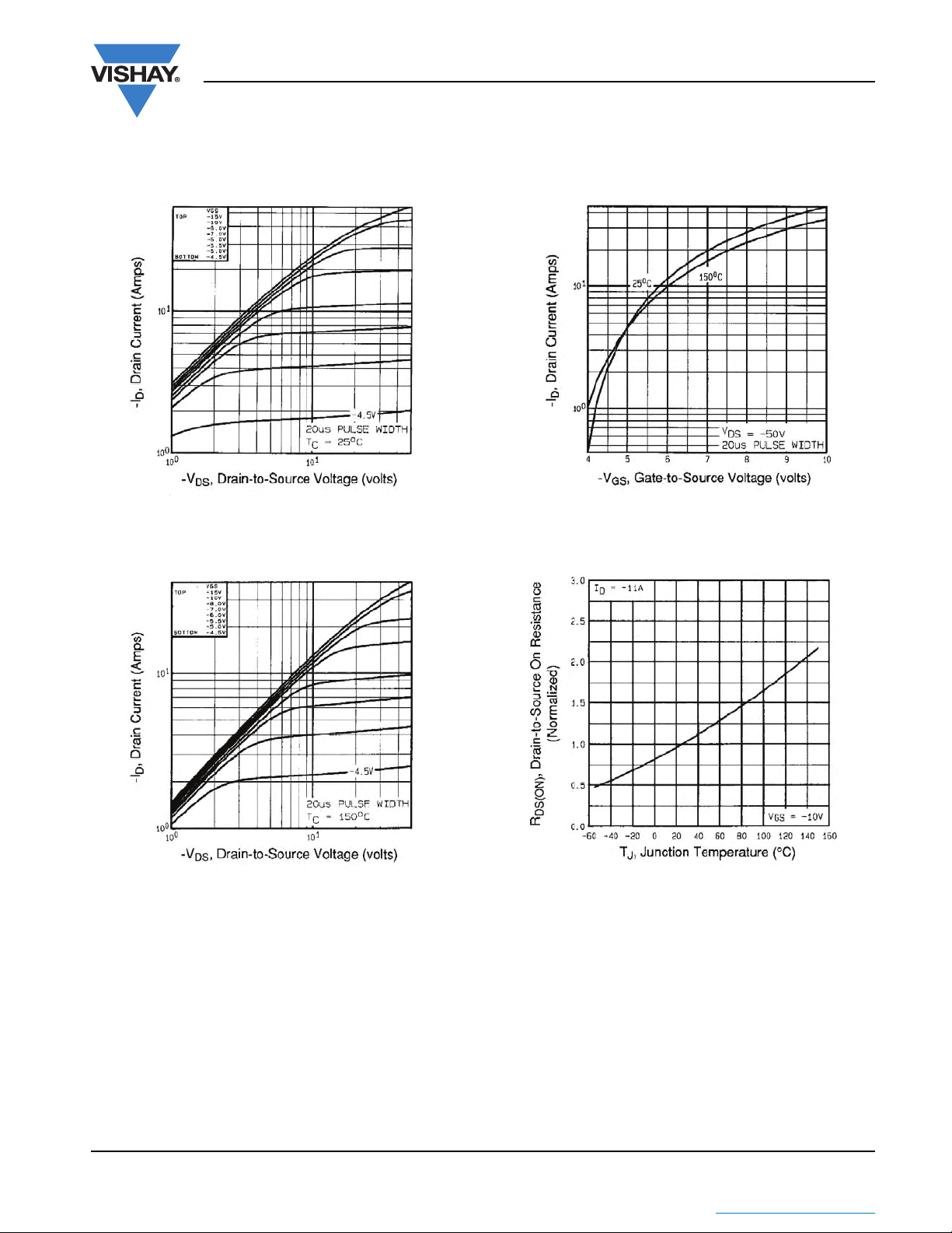
TYPICAL CHARACTERISTICS (25 °C, unless otherwise noted)
IRFP9240, SiHFP9240
Vishay Siliconix
Fig. 1 - Typical Output Characteristics, TC = 25 °C
Fig. 2 - Typical Output Characteristics, T
= 150 °C
C
Fig. 3 - Typical Transfer Characteristics
Fig. 4 - Normalized On-Resistance vs. Temperature
Document Number: 91239 www.vishay.com
S11-0444-Rev. B, 14-Mar-11 3
THE PRODUCT DESCRIBED HEREIN AND THIS DATASHEET ARE SUBJECT TO SPECIFIC DISCLAIMERS, SET FORTH AT
This datasheet is subject to change without notice.
www.vishay.com/doc?91000
 Loading...