

Vishay IRFBC30AS, SiHFBC30AS, IRFBC30AL, SiHFBC30AL Data Sheet
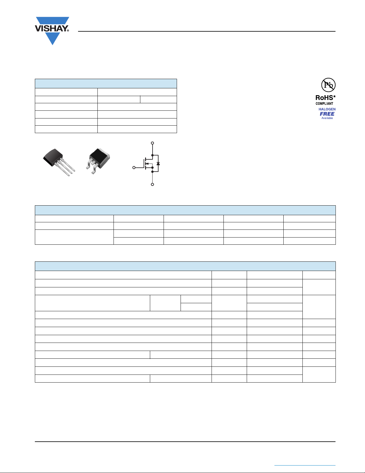
D2PAK (TO-263)
G
D
S
I2PAK (TO-262)
IRFBC30AS, SiHFBC30AS, IRFBC30AL, SiHFBC30AL
Vishay Siliconix
Power MOSFET
PRODUCT SUMMARY
VDS (V) 600
R
()V
DS(on)
Q
(Max.) (nC) 23
g
Q
(nC) 5.4
gs
Q
(nC) 11
gd
Configuration Single
= 10 V 2.2
GS
D
FEATURES
• Halogen-free According to IEC 61249-2-21
Definition
• Low Gate Charge Q
Requirement
• Improved Gate, Avalanche and Dynamic dV/dt
Ruggedness
• Fully Characterized Capacitance and Avalanche Voltage
and Current
• Effective C
Specified
oss
Results in Simple Drive
g
• Compliant to RoHS Directive 2002/95/EC
APPLICATIONS
G
S
N-Channel MOSFET
• Switch Mode Power Supply (SMPS)
• Uninterruptible Power Supply
• High Speed Power Switching
TYPICAL SMPS TOPOLOGIES
• Single Transistor Flyback
ORDERING INFORMATION
Package D2PAK (TO-263) D2PAK (TO-263) D2PAK (TO-263) I2PAK (TO-262)
Lead (Pb)-free and Halogen-free SiHFBC30AS-GE3 SiHFBC30ASTRL-GE3
Lead (Pb)-free
IRFBC30ASPbF IRFBC30ASTRLPbF
SiHFBC30AS-E3 SiHFBC30ASTL-E3
Note
a. See device orientation.
a
SiHFBC30ASTRR-GE3aSiHFBC30AL-GE3
a
IRFBC30ASTRRPbF
a
SiHFBC30ASTR-E3
a
IRFBC30ALPbF
a
SiHFBC30AL-E3
ABSOLUTE MAXIMUM RATINGS (TC = 25 °C, unless otherwise noted)
PARAMETER SYMBOL LIMIT UNIT
Drain-Source Voltage V
Gate-Source Voltage V
T
= 25 °C
Continuous Drain Current V
Pulsed Drain Current
a, e
at 10 V
GS
C
= 100 °C 2.3
C
DS
± 30
GS
I
D
IDM 14
Linear Derating Factor 0.69 W/°C
c, e
b
a
= 25 °C P
C
Single Pulse Avalanche Energy
Avalanche Current
a
Repetiitive Avalanche Energy
Maximum Power Dissipation T
Peak Diode Recovery dV/dt
Operating Junction and Storage Temperature Range T
E
AS
I
AR
E
AR
D
dV/dt 7.0 V/ns
, T
J
stg
Soldering Recommendations (Peak Temperature) for 10 s 300
Notes
a. Repetitive rating; pulse width limited by maximum junction temperature (see fig. 11).
b. Starting T
c. I
SD
d. 1.6 mm from case.
e. Uses IRFBC30A/SiHFBC30A data and test conditions.
* Pb containing terminations are not RoHS compliant, exemptions may apply
Document Number: 91109
S11-1052-Rev. C, 30-May-11 1
= 25 °C, L = 46 mH, Rg = 25 , IAS = 3.6 A (see fig. 12).
J
3.6 A, dI/dt 170 A/μs, VDD VDS, TJ 150 °C.
www.vishay.com
This document is subject to change without notice.
THE PRODUCTS DESCRIBED HEREIN AND THIS DOCUMENT ARE SUBJECT TO SPECIFIC DISCLAIMERS, SET FORTH AT
600
3.6
290 mJ
3.6 A
7.4 mJ
74 W
- 55 to + 150
d
www.vishay.com/doc?91000
V
AT
°C
IRFBC30AS, SiHFBC30AS, IRFBC30AL, SiHFBC30AL
Vishay Siliconix
THERMAL RESISTANCE RATINGS
PARAMETER SYMBOL TYP. MAX. UNIT
Maximum Junction-to-Ambient (PCB
Mounted, steady-state)
a
Maximum Junction-to-Case (Drain) R
Note
a. When mounted on 1" square PCB (FR-4 or G-10 material).
SPECIFICATIONS (TJ = 25 °C, unless otherwise noted)
PARAMETER SYMBOL TEST CONDITIONS MIN. TYP. MAX. UNIT
Static
Drain-Source Breakdown Voltage V
V
Temperature Coefficient VDS/TJ Reference to 25 °C, ID = 1 mA
DS
Gate-Source Threshold Voltage V
Gate-Source Leakage I
Zero Gate Voltage Drain Current I
Drain-Source On-State Resistance R
Forward Transconductance g
Dynamic
Input Capacitance C
Output Capacitance C
Reverse Transfer Capacitance C
Output Capacitance C
Effective Output Capacitance C
Total Gate Charge Q
Gate-Drain Charge Q
Turn-On Delay Time t
Rise Time t
Turn-Off Delay Time t
Fall Time t
Drain-Source Body Diode Characteristics
Continuous Source-Drain Diode Current I
Pulsed Diode Forward Current
Body Diode Voltage V
Body Diode Reverse Recovery Time t
Body Diode Reverse Recovery Charge Q
Forward Turn-On Time t
Notes
a. Repetitive rating; pulse width limited by maximum junction temperature (see fig. 11).
b. Pulse width 300 μs; duty cycle 2 %.
c. C
eff. is a fixed capacitance that gives the same charging time as C
oss
d. Uses IRFBC30A/SiHFBC30A data and test conditions.
www.vishay.com Document Number: 91109
2 S11-1052-Rev. C, 30-May-11
THE PRODUCTS DESCRIBED HEREIN AND THIS DOCUMENT ARE SUBJECT TO SPECIFIC DISCLAIMERS, SET FORTH AT
a
R
thJA
thJC
DS
GS(th)
V
GSS
-40
-1.7
VGS = 0, ID = 250 μA 600 - - V
d
-0.67-V/°C
VDS = VGS, ID = 250 μA 2.0 - 4.5 V
= ± 30 V - - ± 100 nA
GS
VDS = 600 V, VGS = 0 V - - 25
DSS
VGS = 10 V ID = 2.2 A
DS(on)
fs
iss
-70-
oss
-3.5-
rss
oss
eff. VDS = 0 V to 480 V
oss
g
--5.4
gs
--11
gd
d(on)
r
-19-
d(off)
-12-
f
S
I
SM
SD
rr
rr
on
V
= 480 V, VGS = 0 V, TJ = 125 °C - - 250
DS
b
--2.2
VDS = 50 V, ID = 2.2 A 2.1 - - S
- 510 -
-31-
f = 1.0 MHz, see fig. 5
V
= 0 V
GS
VGS = 0 V,
V
= 25 V,
DS
V
= 1.0 V, f = 1.0 MHz - 730 -
DS
= 480 V, f = 1.0 MHz - 19 -
V
DS
c
--23
= 3.6 A, VDS = 480 V,
I
V
GS
= 10 V
D
see fig. 6 and 13
b
-9.8-
V
= 300 V, ID = 3.6 A,
DD
R
= 12 , RD = 82 , see fig. 10
g
b, d
MOSFET symbol
showing the
integral reverse
G
p - n junction diode
TJ = 25 °C, IS = 3.6 A, VGS = 0 V
b
TJ = 25 °C, IF = 3.6 A, dI/dt = 100 A/μs
D
S
-13-
--3.6
--14
--1.6V
- 400 600 ns
b,
-1.11.7μC
Intrinsic turn-on time is negligible (turn-on is dominated by LS and LD)
while VDS is rising from 0 to 80 % VDS.
oss
This document is subject to change without notice.
www.vishay.com/doc?91000
°C/W
μA
pF
nC Gate-Source Charge Q
ns
A
0.01
0.1
1
10
100
0.1 1 10 100
20µs PULSE WIDTH
T = 25 C
J
°
TOP
BOTTOM
VGS
15V
10V
8.0V
7.0V
6.0V
5.5V
5.0V
4.5V
V , Drain-to-Source Voltage (V)
I , Drain-to-Source Current (A)
DS
D
4.5V
0.1
1
10
0.1 1 10 100
20µs PULSE WIDTH
T = 150 C
J
°
TOP
BOTTOM
VGS
15V
10V
8.0V
7.0V
6.0V
5.5V
5.0V
4.5V
V , Drain-to-Source Voltage (V)
I , Drain-to-Source Current (A)
DS
D
4.5V
IRFBC30AS, SiHFBC30AS, IRFBC30AL, SiHFBC30AL
TYPICAL CHARACTERISTICS (25 °C, unless otherwise noted)
Vishay Siliconix
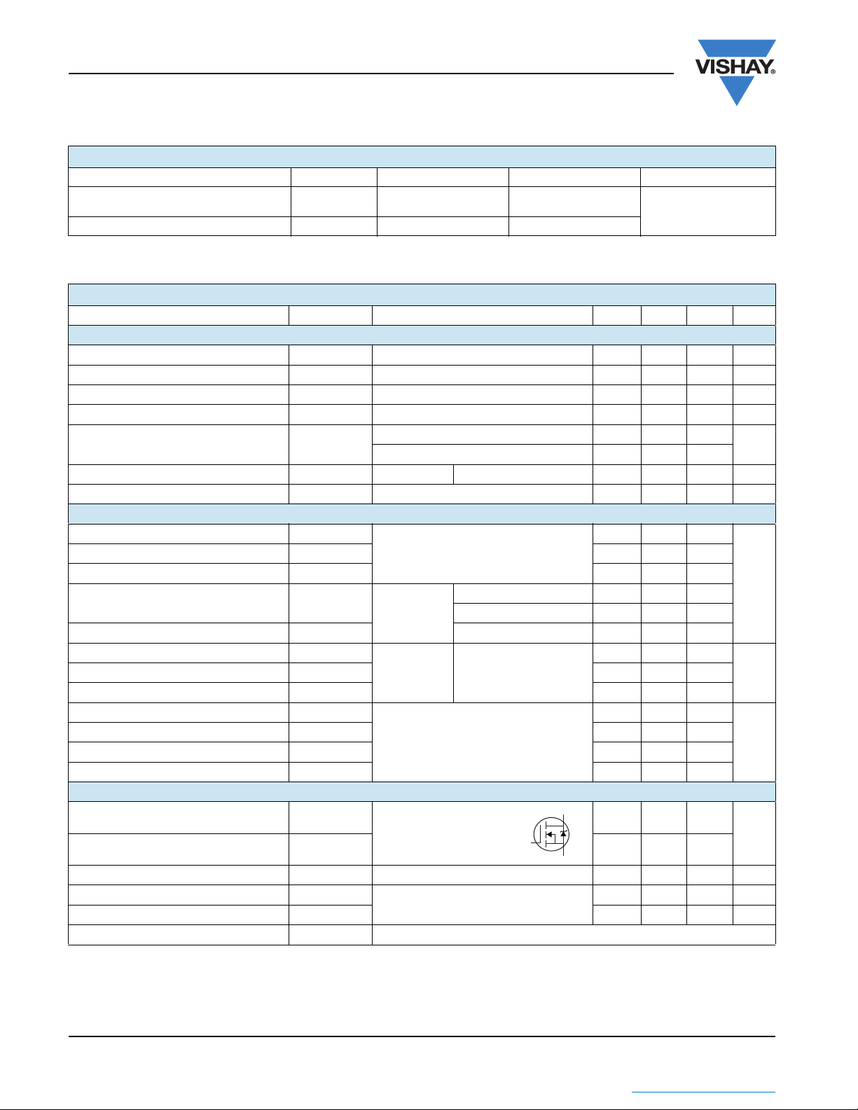
100
10
°
T = 150 C
J
1
°
T = 25 C
0.1
D
I , Drain-to-Source Current (A)
0.01
4.0 5.0 6.0 7.0 8.0 9.0
J
V = 50V
DS
20µs PULSE WIDTH
V , Gate-to-Source Voltage (V)
GS
Fig. 1 - Typical Output Characteristics
Fig. 2 - Typical Output Characteristics
Fig. 3 - Typical Transfer Characteristics
3.0
2.5
2.0
1.5
(Normalized)
1.0
0.5
DS(on)
R , Drain-to-Source On Resistance
0.0
3.6A
I =
D
V =
GS
-60 -40 -20 0 20 40 60 80 100 120 140 160
T , Junction Temperature ( C)
J
°
Fig. 4 - Normalized On-Resistance vs. Temperature
10V
Document Number: 91109 www.vishay.com
S11-1052-Rev. C, 30-May-11 3
THE PRODUCTS DESCRIBED HEREIN AND THIS DOCUMENT ARE SUBJECT TO SPECIFIC DISCLAIMERS, SET FORTH AT
This document is subject to change without notice.
www.vishay.com/doc?91000
1 10 100 1000
VDS, Drain-to-Source Voltage (V)
1
10
100
1000
10000
C
,
C
a
p
a
c
i
t
a
n
c
e
(
p
F
)
Coss
Crss
Ciss
V
GS
= 0V, f = 1 MHZ
C
iss
= C
gs
+ Cgd, C
ds
SHORTED
C
rss
= C
gd
C
oss
= C
ds
+ C
gd
0 4 8 12 16 20 24
0
4
8
12
16
20
Q , Total Gate Charge (nC)
V , Gate-to-Source Voltage (V)
G
GS
FOR TEST CIRCUIT
SEE FIGURE
I =
D
13
3.6A
V = 120V
DS
V = 300V
DS
V = 480V
DS
0.1
1
10
100
0.4 0.6 0.8 1.0 1.2
V ,Source-to-Drain Voltage (V)
I , Reverse Drain Current (A)
SD
SD
V = 0 V
GS
T = 25 C
J
°
T = 150 C
J
°
0.1
1
10
100
10 100 1000 10000
OPERATION IN THIS AREA LIMITED
BY R
DS(on)
Single Pulse
T T= 150 C
= 25 C
°
°
J
C
V , Drain-to-Source Voltage (V)
I , Drain Current (A)I , Drain Current (A)
DS
D
10us
100us
1ms
10ms
IRFBC30AS, SiHFBC30AS, IRFBC30AL, SiHFBC30AL
Vishay Siliconix
Fig. 5 - Typical Capacitance vs. Drain-to-Source Voltage
www.vishay.com Document Number: 91109
4 S11-1052-Rev. C, 30-May-11
THE PRODUCTS DESCRIBED HEREIN AND THIS DOCUMENT ARE SUBJECT TO SPECIFIC DISCLAIMERS, SET FORTH AT
Fig. 6 - Typical Gate Charge vs. Gate-to-Source Voltage
Fig. 7 - Typical Source-Drain Diode Forward Voltage
Fig. 8 - Maximum Safe Operating Area
This document is subject to change without notice.
www.vishay.com/doc?91000
 Loading...