

Small Signal Zener Diodes, Dual
Features
• These diodes are available in other case
styles and configurations including: the
dual diode common anode configuration
with type designation AZ23, the single
diode SOT23 case with the type designation
BZX84C-V, and the single diode SOD123 case
with the type designation
BZT52C-V.
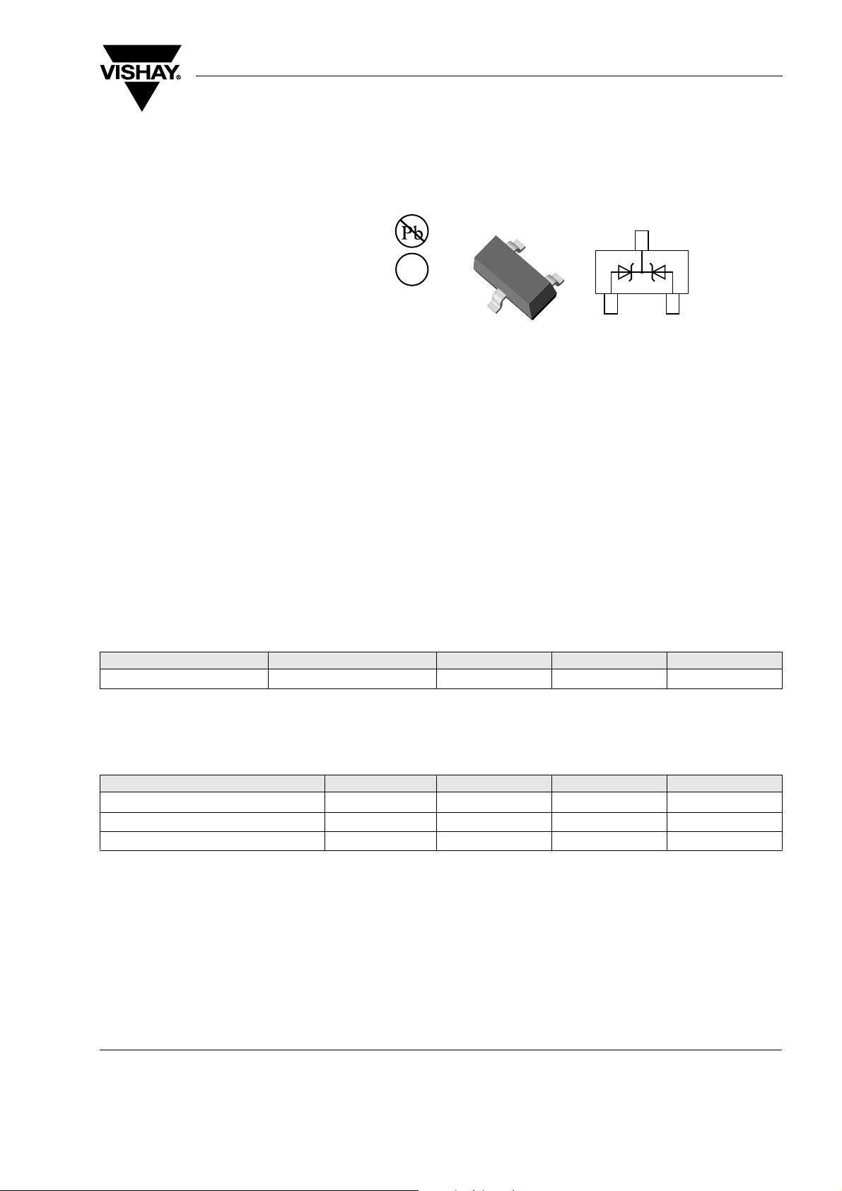
• Dual Silicon Planar Zener Diodes, Common
Cathode
• The Zener voltages are graded according to the
international E 24 standard. Standard Zener voltage tolerance is ± 5 %. Replace "C" with "B" for
2 % tolerance.
• The parameters are valid for both diodes in one
case. ΔV
and Δrzj of the two diodes in one case is
Z
≤ 5 %
• Lead (Pb)-free component
• Component in accordance to RoHS 2002/95/EC
and WEEE 2002/96/EC
e3
DZ23-V-Series
Vishay Semiconductors
3
12
Mechanical Data
Case: SOT23 Plastic case
Weight: approx. 8.8 mg
Packaging Codes/Options:
GS18 / 10 k per 13" reel, (8 mm tape), 10 k/box
GS08 / 3 k per 7" reel, (8 mm tape), 15 k/box
18110
Absolute Maximum Ratings
T
= 25 °C, unless otherwise specified
amb
Parameter Test condition Symbol Val ue Unit
Power dissipation P
1)
Device on fiberglass substrate, see layout on page 7.
Thermal Characteristics
T
= 25 °C, unless otherwise specified
amb
Parameter Test condition Symbol Val ue Unit
Thermal resistance junction to ambient air R
Junction temperature T
Storage temperature range T
1)
Device on fiberglass substrate, see layout on page 7.
tot
thJA
stg
1)
300
1)
420
j
150 °C
- 65 to + 150 °C
mW
K/W
Document Number 85765
Rev. 1.6, 29-Mar-06
www.vishay.com
1

DZ23-V-Series
Vishay Semiconductors
Electrical Characteristics
Partnumber Marking
Code
DZ23C2V7-V V1 2.5 2.9 75 (< 83) < 500 5 - 9 - 4 -
DZ23C3V0-V V2 2.8 3.2 80 (< 95) < 500 5 - 9 - 3 -
DZ23C3V3-V V3 3.1 3.5 80 (< 95) < 500 5 - 8 - 3 -
DZ23C3V6-V V4 3.4 3.8 80 (< 95) < 500 5 - 8 - 3 -
DZ23C3V9-V V5 3.7 4.1 80 (< 95) < 500 5 - 7 - 3 -
DZ23C4V3-V V6 4 4.6 80 (< 95) < 500 5 - 6 - 1 -
DZ23C4V7-V V7 4.4 5 70 (< 78) < 500 5 - 5 2 -
DZ23C5V1-V V8 4.8 5.4 30 (< 60) < 480 5 - 3 4 > 0.8
DZ23C5V6-V V9 5.2 6 10 (< 40) < 400 5 - 2 6 > 1
DZ23C6V2-V V10 5.8 6.6 4.8 (< 10) < 200 5 - 1 7 > 2
DZ23C6V8-V V11 6.4 7.2 4.5 (< 8) < 150 5 2 7 > 3
DZ23C7V5-V V12 7 7.9 4 (< 7) < 50 5 - 3 7 > 5
DZ23C8V2-V V13 7.7 8.7 4.5 (< 7) < 50 5 4 7 > 6
DZ23C9V1-V V14 8.5 9.6 4.8 (< 10) < 50 5 5 8 > 7
DZ23C10-V V15 9.4 10.6 5.2 (< 15) < 70 5 5 8 > 7.5
DZ23C11-V V16 10.4 11.6 6 (< 20) < 70 5 5 9 > 8.5
DZ23C12-V V17 11.4 12.7 7 (< 20) < 90 5 6 9 > 9
DZ23C13-V V18 12.4 14.1 9 (< 25) < 110 5 7 9 > 10
DZ23C15-V V19 13.8 15.6 11 (< 30) < 110 5 7 9 > 11
DZ23C16-V V20 15.3 17.1 13 (< 40) < 170 5 8 9.5 > 12
DZ23C18-V V21 16.8 19.1 18 (< 50) < 170 5 8 9.5 > 14
DZ23C20-V V22 18.8 21.2 20 (< 50) < 220 5 8 10 > 15
DZ23C22-V V23 20.8 23.3 25 (< 55) < 220 5 8 10 > 17
DZ23C24-V V24 22.8 25.6 28 (< 80) < 220 5 8 10 > 18
DZ23C27-V V25 25.1 28.9 30 (< 80) < 250 5 8 10 > 20
DZ23C30-V V26 28 32 35 (< 80) < 250 5 8 10 > 22.5
DZ23C33-V V27 31 35 40 (< 80) < 250 5 8 10 > 25
DZ23C36-V V28 34 38 40 (< 90) < 250 5 8 10 > 27
DZ23C39-V V29 37 41 50 (< 90) < 300 5 10 12 > 29
DZ23C43-V V30 40 46 60 (< 100) < 700 5 10 12 > 32
DZ23C47-V V31 44 50 70 (< 100) < 750 5 10 12 > 35
DZ23C51-V V32 48 54 70 (< 100) < 750 5 10 12 > 38
1)
Tested with pulses tp = 5 ms
Zener Voltage Range
VZ at I
V Ω mA
min max min max
1)
Dynamic Resistance Te st
Current
Z
rzj at
= 5 mA,
I
Z
f = 1 kHz,
rzj at
= 1 mA,
I
Z
f = 1 kHz,
I
Z
Temperature
Coefficient of Zener
Voltage
αVZ at IZ = 5 mA VR at
10-4/°C
Reverse
Vol tage
= 100
I
R
nA
V
www.vishay.com
2
Document Number 85765
Rev. 1.6, 29-Mar-06

DZ23-V-Series
Vishay Semiconductors
Electrical Characteristics
Partnumber Marking
Code
DZ23B2V7-V V1 2.65 2.75 75 (< 83) < 500 5 - 9 - 4 -
DZ23B3V0-V V2 2.94 3.06 80 (< 95) < 500 5 - 9 - 3 -
DZ23B3V3-V V3 3.23 3.37 80 (< 95) < 500 5 - 8 - 3 -
DZ23B3V6-V V4 3.53 3.67 80 (< 95) < 500 5 - 8 - 3 -
DZ23B3V9-V V5 3.82 3.98 80 (< 95) < 500 5 - 7 - 3 -
DZ23B4V3-V V6 4.21 4.39 80 (< 95) < 500 5 - 6 - 1 -
DZ23B4V7-V V7 4.61 4.79 70 (< 78) < 500 5 - 5 2 -
DZ23B5V1-V V8 5 5.2 30 (< 60) < 480 5 - 3 4 > 0.8
DZ23B5V6-V V9 5.49 5.71 10 (< 40) < 400 5 - 2 6 > 1
DZ23B6V2-V V10 6.08 6.32 4.8 (< 10) < 200 5 - 1 7 > 2
DZ23B6V8-V V11 6.66 6.94 4.5 (< 8) < 150 5 2 7 > 3
DZ23B7V5-V V12 7.35 7.65 4 (< 7) < 50 5 - 3 7 > 5
DZ23B8V2-V V13 8.04 8.36 4.5 (< 7) < 50 5 4 7 > 6
DZ23B9V1-V V14 8.92 9.28 4.8 (< 10) < 50 5 5 8 > 7
DZ23B10-V V15 9.8 10.2 5.2 (< 15) < 70 5 5 8 > 7.5
DZ23B11-V V16 10.8 11.2 6 (< 20) < 70 5 5 9 > 8.5
DZ23B12-V V17 11.8 12.2 7 (< 20) < 90 5 6 9 > 9
DZ23B13-V V18 12.7 13.3 9 (< 25) < 110 5 7 9 > 10
DZ23B15-V V19 14.7 15.3 11 (< 30) < 110 5 7 9 > 11
DZ23B16-V V20 15.7 16.3 13 (< 40) < 170 5 8 0.5 > 12
DZ23B18-V V21 17.6 18.4 18 (< 50) < 170 5 8 0.5 > 14
DZ23B20-V V22 19.6 20.4 20 (< 50) < 220 5 8 10 > 15
DZ23B22-V V23 21.6 22.4 25 (< 55) < 220 5 8 10 > 17
DZ23B24-V V24 23.5 24.5 28 (< 80) < 220 5 8 10 > 18
DZ23B27-V V25 26.5 27.5 30 (< 80) < 250 5 8 10 > 20
DZ23B30-V V26 29.4 30.6 35 (< 80) < 250 5 8 10 > 22.5
DZ23B33-V V27 32.3 33.7 40 (< 80) < 250 5 8 10 > 25
DZ23B36-V V28 35.3 36.7 40 (< 90) < 250 5 8 10 > 27
DZ23B39-V V29 38.2 39.8 50 (< 90) < 300 5 10 12 > 29
DZ23B43-V V30 42.1 43.9 60 (< 100) < 700 5 10 12 > 32
DZ23B47-V V31 46.1 47.9 70 (< 100) < 750 5 10 12 > 35
DZ23B51-V V32 50 52 70 (< 100) < 750 5 10 12 > 38
1)
Tested with pulses tp = 5 ms
Zener Voltage Range
VZ at I
V Ω mA
min max min max
1)
Dynamic Resistance Te s t
Current
Z
rzj at
= 5 mA,
I
Z
f = 1 kHz,
rzj at
= 1 mA,
I
Z
f = 1 kHz,
I
Z
Temperature
Coefficient of Zener
Vol tage
αVZ at IZ = 5 mA VR at
10-4/°C
Reverse
Voltage
= 100
I
R
nA
V
Document Number 85765
Rev. 1.6, 29-Mar-06
www.vishay.com
3

DZ23-V-Series
Vishay Semiconductors
Typical Characteristics
T
= 25 °C, unless otherwise specified
amb
mA
3
10
2
10
I
10
F
1
-1
10
-2
10
-3
10
-4
10
-5
10
18114
Figure 1. Forward characteristics
TJ = 100 °C
0 0.2 0.4 0.6 0.8 1 V
= 25 °C
T
J
V
r
1000
zj
5
4
3
2
TJ = 25 °C
100
5
4
3
2
100
5
4
3
2
1
0.1
25 25
F
18117
110
25
I
Z
2.7
3.6
4.7
5.1
5.6
100 mA
Figure 4. Dynamic Resistance vs. Zener Current
mW
500
400
P
tot
300
200
100
0
0 100 200 °C
18115
T
amb
Figure 2. Admissible Power Dissipation vs. Ambient Temperature
°C/W
3
10
7
5
4
3
r
0.5
2
thA
2
0.2
10
7
0.1
5
0.05
4
3
0.02
2
0.01
10
18116
= 0
7
5
4
3
2
1
10-510-410-310-210-1110s
tp
tp
T
T
tp
P
I
Figure 3. Pulse Thermal Resistance vs. Pulse Duration
pF
1000
7
5
4
C
tot
3
2
VR = 1 V
VR = 2 V
TJ = 25 °C
100
18118
7
5
VR = 2 V
4
3
2
10
1
2345 2345
VR = 1 V
10 100 V
VZ at IZ = 5 mA
Figure 5. Capacitance vs. Zener Voltage
Ω
100
5
4
3
r
zj
2
10
5
4
3
2
1
0.1 25 25110
18119
= 25 °C
T
J
33
27
22
18
15
12
10
6.8/8.2
25100 mA
I
Z
6.2
Figure 6. Dynamic Resistance vs. Zener Current
www.vishay.com
4
Document Number 85765
Rev. 1.6, 29-Mar-06

DZ23-V-Series
Vishay Semiconductors
Ω
3
10
7
5
4
r
3
47 + 51
zj
10
10
18120
43
39
2
36
2
7
5
4
3
2
0.1
2345 2345
Tj = 25 °C
1 10 mA
I
Z
Figure 7. Dynamic Resistance vs. Zener Current
Ω
3
10
5
r
= R
zth
4
3
2
r
zth
2
10
5
4
3
2
10
5
4
3
negative
2
1
1
18121
2345 2345
ΔΔV
x VZ x
thA
T
positive
10 100 V
Z
j
VZ at IZ = 5 mA
Figure 8. Thermal Differential Resistance vs. Zener Voltage
mV/°C
25
20
Δ
V
Z
Δ
T
j
15
5 mA
=
I
1 mA
Z
20 mA
10
5
0
- 5
1
2345 2345
18123
10 100 V
V
Z
Figure 10. Temperature Dependence of Zener Voltage vs. Zener
Voltage
V
0.8
0.7
VZ at IZ = 5 mA
0.6
0.5
V
Δ
Z
0.4
0.3
0.2
0.1
0
- 1
- 0.2
020406080
18124
25
15
3.6
100 120 140 C
T
j
10
8
7
6.2
5.9
5.6
5.1
4.7
Figure 11. Change of Zener Voltage vs. Junction Temperature
Ω
100
7
5
4
r
3
zj
2
10
7
5
4
3
2
1
1
2345 2345
18122
Figure 9. Dynamic Resistance vs. Zener Voltage
Document Number 85765
Rev. 1.6, 29-Mar-06
Tj = 25 °C
= 5 mA
I
Z
10 100 V
V
Z
mV/°C
100
80
V
Δ
Z
Δ
T
j
IZ = 5 mA
60
40
20
0
18125
0
20 40 80
60 100 V
V
Z
Figure 12. Temperature Dependence of Zener Voltage vs. Zener
Voltage
www.vishay.com
5

DZ23-V-Series
Vishay Semiconductors
V
9
8
7
Δ
V
6
Z
5
4
3
51
43
36
2
1
0
- 1
0
20 40 120
18126
60
IZ = 2 mA
80 140 °C
100
T
j
Figure 13. Change of Zener Voltage vs. Junction Temperature
V
1.6
VZ = r
x I
Δ
zth
1.4
Z
1.2
Δ
V
1
Z
0.8
0.6
0.4
0.2
0
- 0.2
- 0.4
18127
1
2345 2345
10 100 V
VZ at IZ = 5 mA
Figure 14. Change of Zener voltage from turn-on up to the point of
thermal equilibrium vs. Zener voltage
mA
50
Tj = 25 °C
40
l
z
2.7
3.9
5.6
4.7
3.3
6.8
30
20
Test Current I
10
0
0 10 V
18111
Z
5 mA
1
2345678 9
V
Z
Figure 16. Breakdown Characteristics
mA
30
l
z
20
10
Test Current I
5 mA
0
0 40 V
18112
10
12
15
18
22
Z
10 20 30
V
Z
27
Figure 17. Breakdown Characteristics
8.2
Tj = 25 °C
33
36
V
5
Δ
= r
x I
V
Z
zth
Z
4
Δ
V
Z
3
IZ = 5 mA
2
18128
1
0
0
20 40 60 80
I
= 2 mA
Z
V
Z
100 V
Figure 15. Change of Zener voltage from turn-on up to the point of
thermal equilibrium vs. Zener voltage
www.vishay.com
6
mA
10
8
l
z
Test Current I
5 mA
6
39
43
Z
51
47
4
2
0
10
0 100 V
18113
20 30 40 50 60 70 8090
V
Z
Figure 18. Breakdown Characteristics
Document Number 85765
Rev. 1.6, 29-Mar-06
Tj = 25 °C

DZ23-V-Series
Vishay Semiconductors
Layout for R
thJA
test
Thickness: Fiberglass 0.059 in. (1.5 mm)
Copper leads 0.012 in. (0.3 mm)
12 (0.47)
15 (0.59)
0.8 (0.03)
5 (0.2)
Package Dimensions in mm (Inches)
7.5 (0.3)
3 (0.12)
1.5 (0.06)
5.1 (0.2)
1 (0.4)
2 (0.8)
1 (0.4)
2 (0.8)
17451
Document Number 85765
Rev. 1.6, 29-Mar-06
17418
www.vishay.com
7

DZ23-V-Series
Vishay Semiconductors
Ozone Depleting Substances Policy Statement
It is the policy of Vishay Semiconductor GmbH to
1. Meet all present and future national and international statutory requirements.
2. Regularly and continuously improve the performance of our products, processes, distribution and operating
systems with respect to their impact on the health and safety of our employees and the public, as well as
their impact on the environment.
It is particular concern to control or eliminate releases of those substances into the atmosphere which are
known as ozone depleting substances (ODSs).
The Montreal Protocol (1987) and its London Amendments (1990) intend to severely restrict the use of ODSs
and forbid their use within the next ten years. Various national and international initiatives are pressing for an
earlier ban on these substances.
Vishay Semiconductor GmbH has been able to use its policy of continuous improvements to eliminate the use
of ODSs listed in the following documents.
1. Annex A, B and list of transitional substances of the Montreal Protocol and the London Amendments
respectively
2. Class I and II ozone depleting substances in the Clean Air Act Amendments of 1990 by the Environmental
Protection Agency (EPA) in the USA
3. Council Decision 88/540/EEC and 91/690/EEC Annex A, B and C (transitional substances) respectively.
Vishay Semiconductor GmbH can certify that our semiconductors are not manufactured with ozone depleting
substances and do not contain such substances.
We reserve the right to make changes to improve technical design
and may do so without further notice.
Parameters can vary in different applications. All operating parameters must be validated for each
customer application by the customer. Should the buyer use Vishay Semiconductors products for any
unintended or unauthorized application, the buyer shall indemnify Vishay Semiconductors against all
claims, costs, damages, and expenses, arising out of, directly or indirectly, any claim of personal
damage, injury or death associated with such unintended or unauthorized use.
Vishay Semiconductor GmbH, P.O.B. 3535, D-74025 Heilbronn, Germany
www.vishay.com
8
Document Number 85765
Rev. 1.6, 29-Mar-06

 Loading...