

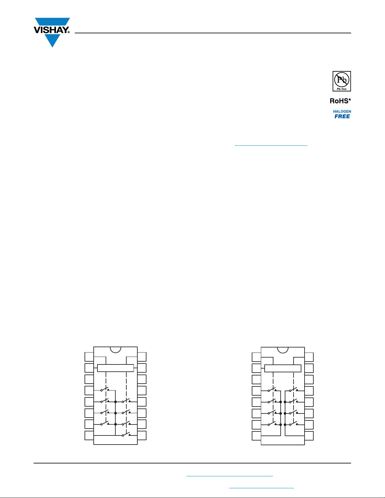
DG408, DG409
S
3
A
0
S
6
D
S
4
A
1
S
8
S
7
EN
Dual-In-Line,
SOIC and TSSOP
A
2
V- GND
S
1
V+
S
2
S
5
Decoders/Drivers
1
2
3
4
5
6
7
16
15
14
13
12
11
10
Top View
89
DG408
Dual-In-Line,
SOIC and TSSOP
9
A
0
D
a
A
1
D
b
EN GND
V- V+
S
1a
S
1b
S
2a
S
2b
S
3a
S
3b
S
4a
S
4b
Decoders/Drivers
1
2
3
4
5
6
7
16
15
14
13
12
11
10
Top View
8
DG409
www.vishay.com
Vishay Siliconix
8-Ch/Dual 4-Ch High-Performance CMOS Analog Multiplexers
DESCRIPTION
The DG408 is an 8 channel single-ended analog multiplexer
designed to connect one of eight inputs to a common output
as determined by a 3-bit binary address (A0, A1, A2). The
DG409 is a dual 4 channel differential analog multiplexer
designed to connect one of four differential inputs to a
common dual output as determined by its 2-bit binary
address (A
protects against momentary crosstalk between adjacent
channels.
An on channel conducts current equally well in both
directions. In the off state each channel blocks voltages up
to the power supply rails. An enable (EN) function allows the
user to reset the multiplexer/demultiplexer to all switches off
for stacking several devices. All control inputs, address (A
and enable (EN) are TTL compatible over the full specified
operating temperature range.
Applications for the DG408, DG409 include high speed data
acquisition, audio signal switching and routing, ATE
systems, and avionics. High performance and low power
dissipation make them ideal for battery operated and
remote instrumentation applications.
Designed in the 44 V silicon-gate CMOS process, the
absolute maximum voltage rating is extended to 44 V.
Additionally, single supply operation is also allowed. An
epitaxial layer prevents latchup.
For additional information please see Technical Article
TA201.
, A1). Break-before-make switching action
0
)
x
FEATURES
• Low on-resistance - R
• Low charge injection - Q: 20 pC
• Fast transition time - t
• Low power - I
SUPPLY
• Single supply capability
• 44 V supply max. rating
• TTL compatible logic
• Material categorization: For definitions of compliance
please see www.vishay.com/doc?99912
Note
*
Thi s datasheet pro vi des information about parts that are
RoHS-compliant and/or parts that are non-RoHS-compliant. For
example, parts with lead (Pb) terminations are not RoHS-compliant.
Please see the information/tables in this datasheet for details.
DS(on)
TRANS
: 10 μA
: 100
: 160 ns
Available
Available
BENEFITS
• Reduced switching errors
• Reduced glitching
• Improved data throughput
• Reduced power consumption
• Increased ruggedness
• Wide supply ranges
- Single supply: +5 V to 36 V
- Dual supplies: ± 5 V to ± 20 V
APPLICATIONS
• Data acquisition systems
• Audio signal routing
• ATE systems
• Battery powered systems
• Single supply systems
• Medical instrumentation
FUNCTIONAL BLOCK DIAGRAM AND PIN CONFIGURATION
S13-2504-Rev. K, 16-Dec-13
THIS DOCUMENT IS SUBJECT TO CHANGE WITHOUT NOTICE. THE PRODUCTS DESCRIBED HEREIN AND THIS DOCUMENT
ARE SUBJECT TO SPECIFIC DISCLAIMERS, SET FORTH AT www.vishay.com/doc?91000
For technical questions, contact: analogswitchtechsupport@vishay.com
1
Document Number: 70062
www.vishay.com
DG408, DG409
Vishay Siliconix
TRUTH TABLE (DG408)
A
2
XXX0None
0001 1
0011 2
0101 3
0111 4
1001 5
1011 6
1101 7
1111 8
A
1
A
0
EN ON SWITCH
TRUTH TABLE (DG409)
A
1
XX0None
0011
0112
1013
1114
Notes
• Logic “0” = V
• Logic “1” = V
•X = Do not care
0.8 V
AL
2.4 V
AH
A
0
EN ON SWITCH
ORDERING INFORMATION (Commercial)
PART CONFIGURATION TEMP. RANGE PACKAGE ORDERING PART NUMBER
16-pin plastic DIP
DG408 8:1 x 1 -40 °C to 85 °C
16-pin SOIC
16-pin TSSOP
16-pin plastic DIP
DG409 4:1 x 2 -40 °C to 85 °C
16-pin SOIC
16-pin TSSOP
Note
• -T1 indicates Tape and Reel, -E3 indicates Lead-Free and RoHS Compliant, NO -E3 indicates standard Tin/Lead finish.
DG408DJ
DG408DJ-E3
DG408DY
DG408DY-E3
DG408DY-T1
DG408DY-T1-E3
DG408DQ-E3
DG408DQ-T1-E3
DG409DJ
DG409DJ-E3
DG409DY
DG409DY-E3
DG409DY-T1
DG409DY-T1-E3
DG409DQ-E3
DG409DQ-T1-E3
ABSOLUTE MAXIMUM RATINGS
PARAMETER LIMIT UNIT
Voltages Referenced to V-
a
Digital Inputs
, VS, V
D
Current (any terminal) 30
Peak Current, S or D (pulsed at 1 ms, 10 % duty cycle max.) 100
Storage Temperature (DJ, DY suffix) -65 to 125 °C
Power Dissipation (Package)
b
Notes
a. Signals on S
, DX or INX exceeding V+ or V- will be clamped by internal diodes. Limit forward diode current to maximum current ratings.
X
b. All leads soldered or welded to PC board.
c. Derate 6 mW/°C above 75 °C.
d. Derate 7.6 mW/°C above 75 °C.
e. Also applies when V- = GND.
S13-2504-Rev. K, 16-Dec-13
For technical questions, contact: analogswitchtechsupport@vishay.com
THIS DOCUMENT IS SUBJECT TO CHANGE WITHOUT NOTICE. THE PRODUCTS DESCRIBED HEREIN AND THIS DOCUMENT
ARE SUBJECT TO SPECIFIC DISCLAIMERS, SET FORTH AT www.vishay.com/doc?91000
e
V+ to V-
44
GND to V- -25
(V-) - 2 to (V+) + 2
or 20 mA, whichever occurs first
16-pin plastic DIP
16-pin narrow SOIC and TSSOP
c
d
450
600
2
Document Number: 70062
V
mA
mW
www.vishay.com
DG408, DG409
Vishay Siliconix
SPECIFICATIONS
a
TEST CONDITIONS UNLESS
OTHERWISE SPECIFIED
D SUFFIX
-40 °C to 85 °C
V+ = 15 V, V- = -15 V
PARAMETER SYMBOL
VAL = 0.8 V, VAH = 2.4 V
f
TEMP.
b
TYP.
c
MIN.
d
MAX.
d
UNIT
Analog Switch
Analog Signal Range
Drain-Source
On-Resistance
R
Matching Between
DS(on)
Channels
g
Source Off Leakage Current I
DG408
DG408 Full - -20 20
DG409 Room - -1 1
Drain Off Leakage
Current
DG409 Full - -10 10
DG408
DG408 Full - -20 20
DG409 Room - -1 1
Drain On Leakage
Current
e
V
ANALOG
R
DS(on)
R
DS(on)
S(off)
Full - -15 15 V
VD = ± 10 V, IS = -10 mA
Room 40 - 100
Full - - 125
VD = ± 10 V Room - - 15
= ± 10 V,
V
S
V
= ± 10 V, VEN = 0 V
D
Room - -0.5 0.5
Full - -5 5
Room - -1 1
= ± 10 V,
V
I
D(off)
D
V
= ± 10 V,
S
V
= 0 V
EN
nA
Room - -1 1
= VD = ± 10 V
V
I
D(on)
S
sequence each
switch on
DG409 Full - -10 10
Digital Control
Logic High Input Voltage V
Logic Low Input Voltage V
Logic High Input Current I
Logic Low Input Current I
Logic Input Capacitance C
INH
INL
AH
AL
f = 1 MHz Room 8 - - pF
in
VA = 2.4 V, 15 V Full - -10 10
VEN = 0 V, 2.4 V, VA = 0 V Full - -10 10
Full - 2.4 -
Full - - 0.8
μA
Dynamic Characteristics
Transition Time t
Break-Before-Make Interval t
Enable Turn-On Time t
Enable Turn-Off Time t
Charge Injection Q C
Off Isolation
h
Source Off Capacitance C
DG408
DG409 Room 14 - -
DG408
DG409 Room 25 - -
Drain Off
Capacitance
Drain On
Capacitance
see figure 2 Full 160 - 250
TRANS
OPEN
ON(EN)
OFF(EN)
OIRR
S(off)
C
D(off)
C
D(on)
see figure 4 Room - 10 -
Room 115 - 150
see figure 3
Full - - -
Room 105 - 150
= 10 nF, VS = 0 V Room 20 - - pC
L
= 0 V, RL = 1 k,
V
EN
f = 1 MHz
VEN = 0 V, VS = 0 V,
f = 1 MHz
Room -75 - -
Room 3 - -
Room 26 - -
= 0 V,
V
EN
V
= 0 V,
D
f = 1 MHz
Room 37 - -
ns
pF
Power Supplies
Positive Supply Current I+
Negative Supply Current I- Full 1 -75 -
Positive Supply Current I+
= VA = 0 V or 5 V
V
EN
= VA = 0 V or 5 V
V
EN
Full 10 - 75
Room 0.2 - 0.5
Full - - 2
μA
mA
Negative Supply Current I- Full - -500 - μA
V
S13-2504-Rev. K, 16-Dec-13
3
Document Number: 70062
For technical questions, contact: analogswitchtechsupport@vishay.com
THIS DOCUMENT IS SUBJECT TO CHANGE WITHOUT NOTICE. THE PRODUCTS DESCRIBED HEREIN AND THIS DOCUMENT
ARE SUBJECT TO SPECIFIC DISCLAIMERS, SET FORTH AT www.vishay.com/doc?91000
DG408, DG409
www.vishay.com
SPECIFICATIONSa (Single Supply)
TEST CONDITIONS UNLESS
OTHERWISE SPECIFIED
V+ = 12 V, V- = 0 V
PARAMETER SYMBOL
VAL = 0.8 V, VAH = 2.4 V
f
TEMP.
b
Analog Switch
Drain-Source
On-Resistance
e,f
R
DS(on)
VD = 3 V, 10 V, IS = -1 mA Room 90 - -
Dynamic Characteristics
Switching Time of
Multiplexer
e
Enable Turn-On Time
Enable Turn-Off Time
Charge Injection
e
e
e
t
VS1 = 8 V, VS8 = 0 V, VIN = 2.4 V Room 180 - -
TRANS
V
t
ON(EN)
t
OFF(EN)
QC
= 1 nF, VS = 0 V, RS = 0 Room 5 - - pC
L
= 2.4 V, V
INH
V
S1
= 5 V
INL
= 0 V,
Room 180 - -
Room 120 - -
Notes
a. Refer to PROCESS OPTION FLOWCHART.
b. Room = 25 °C, Full = as determined by the operating temperature suffix.
c. Typical values are for DESIGN AID ONLY, not guaranteed nor subject to production testing.
d. The algebraic convention whereby the most negative value is a minimum and the most positive a maximum, is used in this datasheet.
e. Guaranteed by design, not subject to production test.
= input voltage to perform proper function.
f. V
IN
g. R
DS(on)
= R
DS(on)
max. - R
DS(on)
min.
h. Worst case isolation occurs on channel 4 due to proximity to the drain pin.
Stresses beyond those listed under “Absolute Maximum Ratings” may cause permanent damage to the device. These are stress ratings only, and functional operation
of the device at these or any other conditions beyond those indicated in the operational sections of the specifications is not implied. Exposure to absolute maximum
rating conditions for extended periods may affect device reliability.
TYP.
c
Vishay Siliconix
D SUFFIX
-40 °C to 85 °C
MIN.
d
MAX.
d
UNIT
ns
S13-2504-Rev. K, 16-Dec-13
4
Document Number: 70062
For technical questions, contact: analogswitchtechsupport@vishay.com
THIS DOCUMENT IS SUBJECT TO CHANGE WITHOUT NOTICE. THE PRODUCTS DESCRIBED HEREIN AND THIS DOCUMENT
ARE SUBJECT TO SPECIFIC DISCLAIMERS, SET FORTH AT www.vishay.com/doc?91000
www.vishay.com
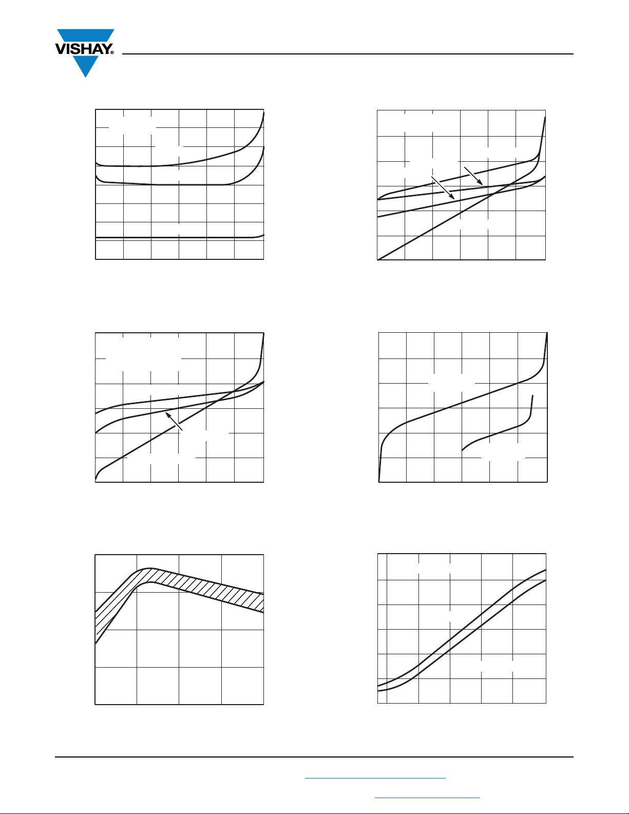
(pF) C
S, D
V
AN AL O G
- Analog Voltage (V)
0 15 - 15
0
20
40
80
60
V+ = 15 V
V- = - 15 V
C
D( of f)
C
S( o f f )
- 10 - 5 5 1 0
C
D( on)
I
S
V
AN AL O G
- Analog Voltage (V)
(pA)
I
D
12 0 10 6 2 4 8
- 60
- 40
- 20
60
40
0
20
DG408 I
D( of f)
DG409 I
D( of f)
DG409 I
D( on)
DG408 I
D( on)
V S = 0 V for I
D( of f)
V S = V D for I
D( on)
S
Switching Frequency (Hz)
10K 10M1 0 0 1K 100K 1M
V
SU PPL Y
= ± 15 V
- 100 mA
- 1 mA
- 100 µA
- 10 µA
- 1 µA
- 0.1 µA
- 10 mA
V
EN
= 2.4 V
V
EN
= 0 V or 5 V
I-
TYPICAL CHARACTERISTICS (25 °C, unless otherwise noted)
DG408, DG409
Vishay Siliconix
Source/Drain Capacitance vs. Analog Voltage
(pA)
D
100
- 20
- 60
- 100
- 140
60
20
V+ = 15 V
V- = - 15 V
= - VD for I
V
S
V D = V
- 10 - 5 5 1 0
V D or V
D(off)
for I
S ( open)
DG409 I
D( on)
D( of f)
DG409 I
DG408 I
D( on)
, I
D( of f)
0 15 - 15
- Drain or Source V oltage (V)
D( on)
Drain Leakage Current vs. Source/Drain Voltage
2.0
1.5
Drain Leakage Current vs. Source/Drain Voltage
(Single 12 V Supply)
20
15
V+ = 15 V
V- = - 15 V
(pA)
S(off)
I
10
5
0
V+ = 12 V
- 5
V- = 0 V
- 10
- 10 - 5 5 1 0
V
0 15 - 15
- Source V oltage (V)
Source Leakage Current vs. Source Voltage
(V)
1.0
TH
V
0.5
0.0
Input Switching Threshold vs. Supply Voltage
S13-2504-Rev. K, 16-Dec-13
THIS DOCUMENT IS SUBJECT TO CHANGE WITHOUT NOTICE. THE PRODUCTS DESCRIBED HEREIN AND THIS DOCUMENT
12 2048 16
+ V
(V)
SUPPLY
Negative Supply Current vs. Switching Frequency
5
For technical questions, contact: analogswitchtechsupport@vishay.com
ARE SUBJECT TO SPECIFIC DISCLAIMERS, SET FORTH AT www.vishay.com/doc?91000
Document Number: 70062
www.vishay.com
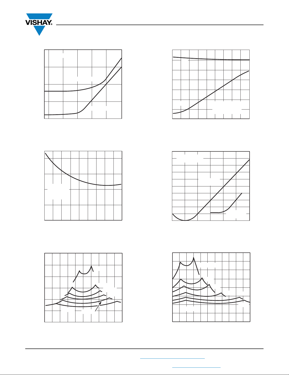
Switching Frequency (Hz)
10K 10M1 0 0 1K 100K 1 M
V
SU PPL Y
= 15 V
100 mA
10 mA
1 mA
100 µA
10 µA
V
EN
= 2.4 V
V
EN
= 0 V or 5 V
I+
I+ (µA)
Temperature (°C)
5
15
20
10
125- 55 85 45 5
0
V+ = 15 V
V- = - 15 V
V
IN
= 0 V
V
EN
= 0 V
- 35 - 15 25 65 105
R
DS(on)
(Ω)
V D - Drain V oltage (V)
0
40
100
60
80
120
20
- 20 - 12 - 8 - 4 0 4 8 1 2 1 6 2 0 - 16
± 5 V
± 8 V
± 10 V
± 12 V
± 20 V
± 15 V
VD - Drain Voltage (V)
220
0
40
100
60
140
160
80
120
20
4 8 12 16 20
V+ = 7.5 V
10 V
12 V
15 V
20 V
22 V
V- = 0 V
R
DS(on)
(Ω)
TYPICAL CHARACTERISTICS (25 °C, unless otherwise noted)
DG408, DG409
Vishay Siliconix
100 µA
Positive Supply Current vs. Switching Frequency
I+, I-
Q (pC)
10 µA
1 µA
100 nA
10 nA
1 nA
100 pA
10 pA
90
80
70
60
50
40
30
20
10
0
- 10
I+
- (I-)
- 35 - 15 25 65 105
Temperature (°C)
I
vs. Temperature
SUPPLY
C L = 10 000 pF
= 5 Vp-p
V
IN
V+ = 15 V
V- = - 15 V
- 10 - 5 5 1 0
V S - Source V oltage (V)
V
= ± 15 V
SU PPL Y
V
= 0 V
A
V
= 0 V
EN
V+ = 12 V
V- = 0 V
0 15- 15
125 - 55 85 45 5
Positive Supply Current vs. Temperature (DG408)
S13-2504-Rev. K, 16-Dec-13
THIS DOCUMENT IS SUBJECT TO CHANGE WITHOUT NOTICE. THE PRODUCTS DESCRIBED HEREIN AND THIS DOCUMENT
R
DS(on)
Charge Injection vs. Analog Voltage
vs. VD and Supply
vs. VD and Supply (Single Supply)
R
DS(on)
6
For technical questions, contact: analogswitchtechsupport@vishay.com
ARE SUBJECT TO SPECIFIC DISCLAIMERS, SET FORTH AT www.vishay.com/doc?91000
Document Number: 70062

www.vishay.com
R
DS(on)
(Ω)
VD - Drain Voltage (V)
0 15 - 15
0
40
60
80
50
10
70
30
20
V+ = 15 V
V- = - 15 V
125 °C
85 °C
25 °C
- 55 °C
- 10 - 5 5 1 0
- 40 °C
0 °C
(
)
150
(
)
SU
R
DS(on)
()
VD - Drain Voltage (V)
4 0
10
30
50
70
90
110
130
V+ = 12 V
V- = 0 V
- 55 °C
- 40 °C
0 °C
125 °C
85 °C
25 °C
2681012
t (ns)
V
SUPPLY
(V)
158
100
150
225
175
200
250
125
91214131110
275
t
TRANS
t
OFF(EN)
t
ON(EN)
TYPICAL CHARACTERISTICS (25 °C, unless otherwise noted)
R
vs. VD and Temperature
DS(on)
DG408, DG409
Vishay Siliconix
R
vs. VD and Temperature (Single Supply)
DS(on)
-
- 130
- 110
- 90
dB
- 70
- 50
- 30
1 0 0 1K 100K 1M
140
120
100
ns
t
80
60
± 10 ± 12 ± 14 ± 16 ± 18 ± 20 ± 22
S13-2504-Rev. K, 16-Dec-13
THIS DOCUMENT IS SUBJECT TO CHANGE WITHOUT NOTICE. THE PRODUCTS DESCRIBED HEREIN AND THIS DOCUMENT
V+ = 15 V
V- = - 15 V
R
= 1 kΩ
L
Of f-Isolation
Crosstalk
10K 10M
f - Frequency (Hz)
Off Isolation and Crosstalk vs. Frequency
t
TRANS
t
OFF(EN)
V
Switching Time vs. Bipolar Supply
ARE SUBJECT TO SPECIFIC DISCLAIMERS, SET FORTH AT www.vishay.com/doc?91000
t
ON(EN)
(V)
PPL Y
For technical questions, contact: analogswitchtechsupport@vishay.com
100M
1
0
- 1
- 2
(dB)
OSS
- 3
L
- 4
- 5
- 6
1 0 1 0 0 1K 10K 100K 1 M 100M
V+ = 15 V
V- = - 15 V
Ref. 1 V
f - Frequency (Hz)
R L = 1 kΩ
RMS
R L = 50 Ω
10M
Insertion Loss vs. Frequency
Switching Time vs. Single Supply
7
Document Number: 70062

www.vishay.com
SCHEMATIC DIAGRAM (Typical Channel)
V+
DG408, DG409
Vishay Siliconix
GND
A
A
0
X
V
EN
V-
TEST CIRCUITS
A
A
A
EN
50 Ω
A
A
EN
50 Ω
REF
2
1
0
1
0
DG408
DG409
V+
+ 15 V
V+
S2 - S
V-GND
- 15 V
+ 15 V
V+
S1a - S4a, D
V-GND
- 15 V
D
V+
Level
Shift
Decode/
Drive
V-
S
1
S
n
Fig. 1
S
1
7
S
8
D
S
1
a
S
4b
D
b
300 Ω
300 Ω
± 10 V
± 10 V
± 10 V
± 10 V
35 pF
35 pF
tr < 20 ns
< 20 ns
t
V
O
Logic
Input
3 V
50 %
f
0 V
V
V
0 V
S1
S8
t
TRANS
1
ON
90 %
S
8
ONS
Switch
Output
V
O
V
O
90 %
t
TRANS
Fig. 2 - Transition Time
S13-2504-Rev. K, 16-Dec-13
8
Document Number: 70062
For technical questions, contact: analogswitchtechsupport@vishay.com
THIS DOCUMENT IS SUBJECT TO CHANGE WITHOUT NOTICE. THE PRODUCTS DESCRIBED HEREIN AND THIS DOCUMENT
ARE SUBJECT TO SPECIFIC DISCLAIMERS, SET FORTH AT www.vishay.com/doc?91000

www.vishay.com
Logic
Input
Switch
Output
V
O
tr < 20 ns
t
f
< 20 ns
3 V
0 V
0 V
t
OFF(EN)
t
ON(EN)
50 %
90 %
10 %
V
O
EN
S
1
S2 - S
8
A
0
A
1
A
2
50 Ω
1 kΩ
V
O
V+
GND V-
D
- 5 V
35 pF
- 15 V
+ 15 V
S
1b
S1a - S4a, D
a
S2b - S
4b
D
b
EN
A
0
A
1
50 Ω
1 kΩ
V
O
V+
GND V-
- 5 V
35 pF
- 15 V
+ 15 V
DG408
DG409
50 %
80 %
Logic
Input
Switch
Output
V
O
V
S
t
OPEN
tr < 20 ns
t
f
< 20 ns
0 V
3 V
0 V
EN
V+
GND V-
+ 5 V
35 pF
- 15 V
+ 15 V
+ 2.4 V
A
2
Db, D
All S and D
a
300 Ω
V
O
50 Ω
A
1
A
0
DG408
DG409
TEST CIRCUITS
DG408, DG409
Vishay Siliconix
S13-2504-Rev. K, 16-Dec-13
THIS DOCUMENT IS SUBJECT TO CHANGE WITHOUT NOTICE. THE PRODUCTS DESCRIBED HEREIN AND THIS DOCUMENT
Fig. 3 - Enable Switching Time
ARE SUBJECT TO SPECIFIC DISCLAIMERS, SET FORTH AT www.vishay.com/doc?91000
Fig. 4 - Break-Before-Make Interval
For technical questions, contact: analogswitchtechsupport@vishay.com
9
Document Number: 70062

www.vishay.com
A
0
EN
A
1
A
2
V
O
V+
GND V-
D
- 15 V
+ 15 V
R
g
S
X
C
L
10 nF
Channel
Select
3 V
0 V
OFF ON
Logic
Input
Switch
Output
ΔV
O
ΔVO is the measured voltage due to charge transfer
error Q, when the channel turns off.
Q = C
L
x ΔV
O
OFF
R
L
1 kΩ
V
O
V+
GND V-
- 15 V
+ 15 V
A
2
D
A
1
A
0
S
8
S
X
V
S
EN
Rg = 50 Ω
Off Isolation = 20 log
V
OUT
V
IN
V
IN
R
L
1 kΩ
A
2
V
O
D
Rg = 50 Ω
Insertion Loss = 20 log
V
OUT
A
1
V
IN
A
0
V
S
S
1
V+
GND V-
- 15 V
+ 15 V
EN
R
L
1 kΩ
V
O
V+
GND V-
- 15 V
+ 15 V
A
2
D
A
1
A
0
S
8
S
X
V
S
EN
R
g
= 50 Ω
Crosstalk = 20 log
V
OUT
V
IN
V
IN
S
1
f = 1 MHz
S
1
D
EN
+ 15 V
- 15 V
GND
V+
V-
Meter
HP4192A
Impedance
Analyzer
or Equivalent
S
8
A
1
A
2
A
0
Channel
Select
TEST CIRCUITS
DG408, DG409
Vishay Siliconix
Fig. 5 - Charge Injection
S13-2504-Rev. K, 16-Dec-13
THIS DOCUMENT IS SUBJECT TO CHANGE WITHOUT NOTICE. THE PRODUCTS DESCRIBED HEREIN AND THIS DOCUMENT
Fig. 6 - Off Isolation
Fig. 7 - Crosstalk
Fig. 8 - Insertion Loss
For technical questions, contact: analogswitchtechsupport@vishay.com
ARE SUBJECT TO SPECIFIC DISCLAIMERS, SET FORTH AT www.vishay.com/doc?91000
10
Fig. 9 - Source Drain Capacitance
Document Number: 70062

www.vishay.com
1N4148
DG408
D
V-
V+
1N4148
S
X
V
g
EN
A
0A1
+ 15 V
(MUX On-Off Control)
Analog
Inputs
(Outputs)
Clock
In
NC
Enable In
Analog
Output
(Input)
+ 15 V - 15 V
DG408
D
EN
GND
DM7493
V+ V-
NC
GND
+ 15 V
Analog
Inputs
(Outputs)
Analog
Outputs
(Inputs)
+ 15 V - 15 V
DG409
GNDV+ V-
Differential
Differential
Clock
In
NC
GND
+ 15 V
NC
6
Reset Enable
J
K
CLK
J
K
CLK
CLEAR CLEAR
Q
S
5
S
7
S
6
S
8
S
1
S
3
S
2
S
4
S
1a
S
3a
S
2a
S
4a
S
1b
S
3b
S
2b
S
4b
D
a
D
b
A0A1A
2
B
IN
A
IN
r01r
02
Q
B
Q
C
Q
D
Q
A
1/2 MM74C73 1/2 MM74C73
Q
Q
Q
8-Channel Sequential Multiplexer/Demultiplexer
Differential 4-Channel Sequential Multiplexer/Demultiplexer
APPLICATION HINTS
Overvoltage Protection
A very convenient form of overvoltage protection consists of
adding two small signal diodes (1N4148, 1N914 type) in
series with the supply pins (see figure 10). This arrangement
effectively blocks the flow of reverse currents. It also floats
the supply pin above or below the normal V+ or V- value. In
this case the overvoltage signal actually becomes the power
DG408, DG409
Vishay Siliconix
supply of the IC. From the point of view of the chip, nothing
has changed, as long as the difference VS - (V-) does not
exceed + 44 V. The addition of these diodes will reduce the
analog signal range to 1 V below V+ and 1 V above V-, but it
preserves the low channel resistance and low leakage
characteristics.
Fig. 10 - Overvoltage Protection Using Blocking Diodes
Vishay Siliconix maintains worldwide manufacturing capability. Products may be manufactured at one of several qualified locations. Reliability data for Silicon
Technology and Package Reliability represent a composite of all qualified locations. For related documents such as package/tape drawings, part marking, and
reliability data, see www.vishay.com/ppg?70062
S13-2504-Rev. K, 16-Dec-13
THIS DOCUMENT IS SUBJECT TO CHANGE WITHOUT NOTICE. THE PRODUCTS DESCRIBED HEREIN AND THIS DOCUMENT
.
For technical questions, contact: analogswitchtechsupport@vishay.com
ARE SUBJECT TO SPECIFIC DISCLAIMERS, SET FORTH AT www.vishay.com/doc?91000
Fig. 11
11
Document Number: 70062

SOIC (NARROW): 16ĆLEAD
JEDEC Part Number: MS-012
131416 15 91012 11
4312 8756
Package Information
Vishay Siliconix
MILLIMETERS INCHES
Dim Min Max Min Max
A
A
B
C
D
E
e
E
H
L
Ĭ
ECN: S-03946—Rev. F, 09-Jul-01
DWG: 5300
1.35 1.75 0.053 0.069
0.10 0.20 0.004 0.008
1
0.38 0.51 0.015 0.020
0.18 0.23 0.007 0.009
9.80 10.00 0.385 0.393
3.80 4.00 0.149 0.157
1.27 BSC 0.050 BSC
5.80 6.20 0.228 0.244
0.50 0.93 0.020 0.037
0_ 8_ 0_ 8_
D
e B
A1
H
C
All Leads
L
Ĭ
0.101 mm
0.004 IN
Document Number: 71194
02-Jul-01
www.vishay.com
1

PDIP: 16ĆLEAD
16 15 14 13 12 11 10 9
12345678
Package Information
Vishay Siliconix
E
E
1
D
S
Q
1
A
A
B
1
e
1
B
L
1
15°
C
e
A
MAX
MILLIMETERS INCHES
Dim Min Max Min Max
A
A
B
B
C
D
E
E
e
1
e
A
L
Q
S
ECN: S-03946—Rev. D, 09-Jul-01
DWG: 5482
3.81 5.08 0.150 0.200
0.38 1.27 0.015 0.050
1
0.38 0.51 0.015 0.020
0.89 1.65 0.035 0.065
1
0.20 0.30 0.008 0.012
18.93 21.33 0.745 0.840
7.62 8.26 0.300 0.325
5.59 7.11 0.220 0.280
1
2.29 2.79 0.090 0.110
7.37 7.87 0.290 0.310
2.79 3.81 0.110 0.150
1.27 2.03 0.050 0.080
1
0.38 1.52 .015 0.060
Document Number: 71261
06-Jul-01
www.vishay.com
1

CERDIP: 16ĆLEAD
S
L
1
16 15 14 13 12 11 10 9
12 3 4 5 6 78
D
E1E
Q
1
A
1
Package Information
Vishay Siliconix
A
L
e
B
1
1
B
MILLIMETERS INCHES
Dim Min Max Min Max
A
A
B
B
C
D
E
E
e
1
e
A
L
L
Q
S
∝
ECN: S-03946—Rev. G, 09-Jul-01
DWG: 5403
4.06 5.08 0.160 0.200
0.51 1.14 0.020 0.045
1
0.38 0.51 0.015 0.020
1.14 1.65 0.045 0.065
1
0.20 0.30 0.008 0.012
19.05 19.56 0.750 0.770
7.62 8.26 0.300 0.325
6.60 7.62 0.260 0.300
1
1
1
2.54 BSC 0.100 BSC
7.62 BSC 0.300 BSC
3.18 3.81 0.125 0.150
3.81 5.08 0.150 0.200
1.27 2.16 0.050 0.085
0.38 1.14 0.015 0.045
0° 15° 0° 15°
C
e
A
∝
Document Number: 71282
03-Jul-01
www.vishay.com
1

20ĆLEAD LCC
Packaging Information
Vishay Siliconix
D
L
1
A
1
A
MILLIMETERS INCHES
Dim Min Max Min Max
A
A
B
e
28
E
1
2
D
E
e
L
L
ECN: S-03946—Rev. B, 09-Jul-01
DWG: 5321
BL
1.37 2.24 0.054 0.088
1.63 2.54 0.064 0.100
1
0.56 0.71 0.022 0.028
8.69 9.09 0.342 0.358
8.69 9.09 0.442 0.358
1.27 BSC 0.050 BSC
1.14 1.40 0.045 0.055
1.96 2.36 0.077 0.093
1
Document Number: 71290
02-Jul-01
www.vishay.com
1

TSSOP: 16-LEAD
Package Information
Vishay Siliconix
ECN: S-61920-Rev. D, 23-Oct-06
DWG: 5624
Document Number: 74417
23-Oct-06
DIMENSIONS IN MILLIMETERS
Symbols
A - 1.10 1.20
A1 0.05 0.10 0.15
A2 - 1.00 1.05
B 0.22 0.28 0.38
C - 0.127 -
D 4.90 5.00 5.10
E 6.10 6.40 6.70
E1 4.30 4.40 4.50
e-0.65-
L 0.50 0.60 0.70
L1 0.90 1.00 1.10
y--0.10
θ10°3°6°
Min Nom Max
www.vishay.com
1

www.vishay.com
RECOMMENDED MINIMUM PAD FOR TSSOP-16
0.193
(4.90)
PAD Pattern
Vishay Siliconix
0.055
(1.40)
0.281
(7.15)
0.014
(0.35)
0.026
(0.65)
Recommended Minimum Pads
Dimensions in inches (mm)
0.012
(0.30)
0.171
(4.35)
Revision: 02-Sep-11
1
Document Number: 63550
THIS DOCUMENT IS SUBJECT TO CHANGE WITHOUT NOTICE. THE PRODUCTS DESCRIBED HEREIN AND THIS DOCUMENT
ARE SUBJECT TO SPECIFIC DISCLAIMERS, SET FORTH AT www.vishay.com/doc?91000

Application Note 826
Vishay Siliconix
RECOMMENDED MINIMUM PADS FOR SO-16
RECOMMENDED MINIMUM PADS FOR SO-16
0.372
(9.449)
0.047
(1.194)
Return to Index
0.246
(6.248)
Return to Index
0.022
(0.559)
0.050
(1.270)
Recommended Minimum Pads
Dimensions in Inches/(mm)
0.028
(0.711)
0.152
(3.861)
APPLICATION NOTE
www.vishay.com Document Number: 72608
24 Revision: 21-Jan-08

Legal Disclaimer Notice
www.vishay.com
Vishay
Disclaimer
ALL PRODUCT, PRODUCT SPECIFICATIONS AND DATA ARE SUBJECT TO CHANGE WITHOUT NOTICE TO IMPROVE
RELIABILITY, FUNCTION OR DESIGN OR OTHERWISE.
Vishay Intertechnology, Inc., its affiliates, agents, and employees, and all persons acting on its or their behalf (collectively,
“Vishay”), disclaim any and all liability for any errors, inaccuracies or incompleteness contained in any datasheet or in any other
disclosure relating to any product.
Vishay makes no warranty, representation or guarantee regarding the suitability of the products for any particular purpose or
the continuing production of any product. To the maximum extent permitted by applicable law, Vishay disclaims (i) any and all
liability arising out of the application or use of any product, (ii) any and all liability, including without limitation special,
consequential or incidental damages, and (iii) any and all implied warranties, including warranties of fitness for particular
purpose, non-infringement and merchantability.
Statements regarding the suitability of products for certain types of applications are based on Vishay’s knowledge of typical
requirements that are often placed on Vishay products in generic applications. Such statements are not binding statements
about the suitability of products for a particular application. It is the customer’s responsibility to validate that a particular
product with the properties described in the product specification is suitable for use in a particular application. Parameters
provided in datasheets and/or specifications may vary in different applications and performance may vary over time. All
operating parameters, including typical parameters, must be validated for each customer application by the customer’s
technical experts. Product specifications do not expand or otherwise modify Vishay’s terms and conditions of purchase,
including but not limited to the warranty expressed therein.
Except as expressly indicated in writing, Vishay products are not designed for use in medical, life-saving, or life-sustaining
applications or for any other application in which the failure of the Vishay product could result in personal injury or death.
Customers using or selling Vishay products not expressly indicated for use in such applications do so at their own risk. Please
contact authorized Vishay personnel to obtain written terms and conditions regarding products designed for such applications.
No license, express or implied, by estoppel or otherwise, to any intellectual property rights is granted by this document or by
any conduct of Vishay. Product names and markings noted herein may be trademarks of their respective owners.
Material Category Policy
Vishay Intertechnology, Inc. hereby certifies that all its products that are identified as RoHS-Compliant fulfill the
definitions and restrictions defined under Directive 2011/65/EU of The European Parliament and of the Council
of June 8, 2011 on the restriction of the use of certain hazardous substances in electrical and electronic equipment
(EEE) - recast, unless otherwise specified as non-compliant.
Please note that some Vishay documentation may still make reference to RoHS Directive 2002/95/EC. We confirm that
all the products identified as being compliant to Directive 2002/95/EC conform to Directive 2011/65/EU.
Vishay Intertechnology, Inc. hereby certifies that all its products that are identified as Halogen-Free follow Halogen-Free
requirements as per JEDEC JS709A standards. Please note that some Vishay documentation may still make reference
to the IEC 61249-2-21 definition. We confirm that all the products identified as being compliant to IEC 61249-2-21
conform to JEDEC JS709A standards.
Revision: 02-Oct-12
1
Document Number: 91000

 Loading...