

查询DG2037供应商
DG2037/2038/2039
New Product
Low-Voltage, Low rON, Dual SPST Analog Switch
FEATURES
D Low Voltage Operation (1.8 V to 5.5 V)
D Low On-Resistance - r
DS(on
): 3.0 W
D Fast Switching - 12 ns
D Low Charge Injection - Q
: 10 pC
INJ
D Low Power Consumption
D TTL/CMOS Compatible
D SOT23-8 and MSOP-8 Packages
DESCRIPTION
The DG2037/2038/2039 are dual single-pole/single-throw
monolithic CMOS analog switch designed for high
performance switching of analog signals. Combining low
power, fast switching, low on-resistance (r
3.0 W @ 2.7 V) and small physical size, the
DG2037/2038/2039 are ideal for portable and battery powered
applications requiring high performance and efficient use of
board space.
BENEFITS
D Reduced Power Consumption
D Simple Logic Interface
D High Accuracy
D Reduce Board Space
DS(on)
Vishay Siliconix
APPLICATIONS
D Cellular Phones
D Communication Systems
D Portable Test Equipment
D Battery Operated Systems
D Sample and Hold Circuits
The DG2037/2038/2039 are built on Vishay Siliconix’s new
high density low voltage process. An epitaxial layer prevents
latchup.
:
Each switch conducts equally well in both directions when on,
and blocks up to the power supply level when off.
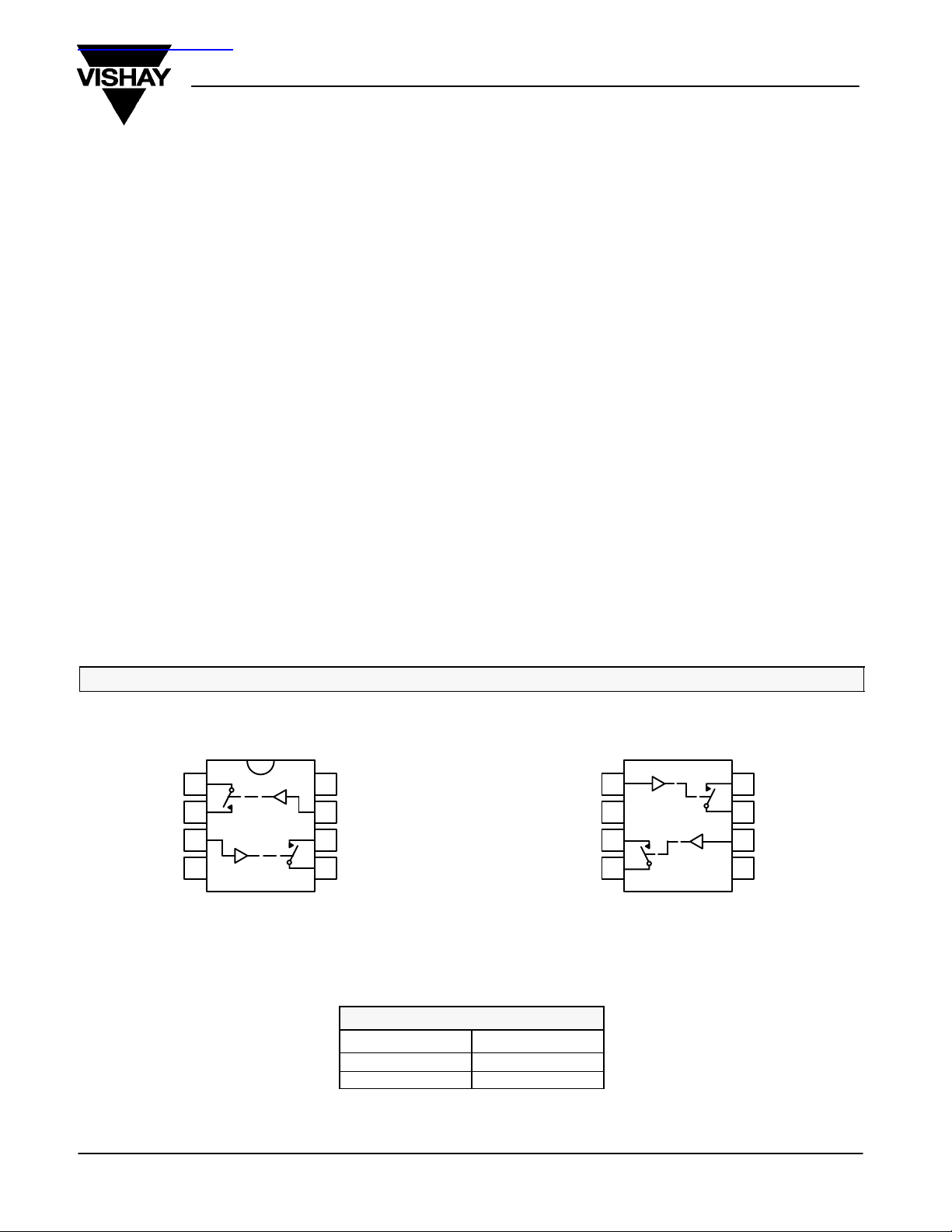
FUNCTIONAL BLOCK DIAGRAM AND PIN CONFIGURATIONDG2037
DG2037, MSOP-8
NO
1
1
COM
1
2
IN
2
3
GND NO
4
Top View
Device Marking: 2037 Device Marking: E0
8
7
6
5
V+
IN
1
COM
2
2
TRUTH TABLE DG2037
Logic Switch
0 Off
1 On
IN
V+
NO
COM
DG2037. SOT23-8
1
1
2
2
3
2
4
Top View
NO
1
8
COM
IN
2
GND
1
7
6
5
Document Number: 72359
S-31642—Rev. A, 01-Aug-03
www.vishay.com
1
DG2037/2038/2039
Vishay Siliconix
New Product
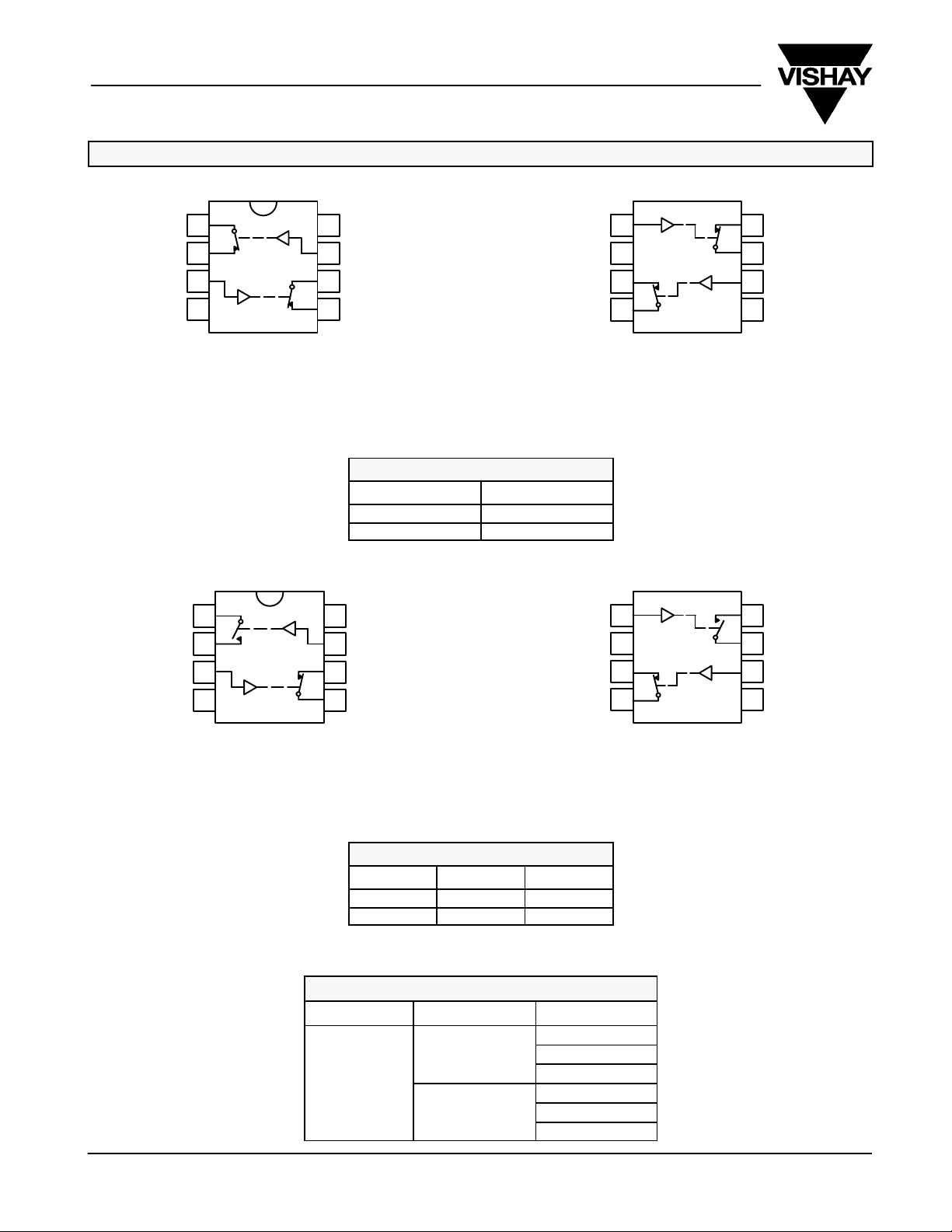
FUNCTIONAL BLOCK DIAGRAM AND PIN CONFIGURATIONDG2038/DG2039
DG2038, MSOP-8
NC
1
1
COM
1
2
IN
2
3
GND NC
4
Top View
Device Marking: 2038 Device Marking: F1
8
7
6
5
V+
IN
1
COM
2
2
TRUTH TABLE DG2038
Logic Switch
0 On
1 Off
IN
V+
NC
COM
DG2038. SOT23-8
1
1
2
2
3
2
4
Top View
NC
1
8
COM
IN
2
GND
1
7
6
5
DG2039, MSOP-8
NO
1
1
COM
1
2
IN
2
3
GND NC
4
Top View
Device Marking: 2039 Device Marking: F2
8
7
6
5
Temp Range Package Part Number
-40 to 85°C
V+
IN
1
COM
2
2
TRUTH TABLE DG2039
Logic Switch-1 Switch-2
0 Off On
1 On Off
ORDERING INFORMATION
MSOP-8
°
SOT23-8
IN
1
V+
NC
2
COM
2
DG2037DQ
DG2038DQ
DG2039DQ
DG2037DS
DG2038DS
DG2039DS
DG2039. SOT23-8
1
2
3
4
Top View
NO
1
8
COM
IN
2
GND
1
7
6
5
www.vishay.com
2
Document Number: 72359
S-31642—Rev. A, 01-Aug-03
DG2037/2038/2039
V+ = 3.3 V
VNO or VNC = 2.0 V, RL = 300 W, CL = 35 pF
IN
p
ABSOLUTE MAXIMUM RATINGS
Reference to GND
V+ -0.3 to 6.0 V. . . . . . . . . . . . . . . . . . . . . . . . . . . . . . . . . . . . . . . . . . . . . . . . . . .
IN, COM, NC, NO
a
-0.3 V to (V+ + 0.3 V). . . . . . . . . . . . . . . . . . . . . . . . . . . . . . . . . . . .
Continuous Current (Any terminal) "50 mA. . . . . . . . . . . . . . . . . . . . . . . . . . .
Peak Current "200 mA. . . . . . . . . . . . . . . . . . . . . . . . . . . . . . . . . . . . . . . . . . . . .
(Pulsed at 1 ms, 10% duty cycle)
Storage Temperature (D Suffix) -65 to 150°C. . . . . . . . . . . . . . . . . . . . . . . . . . . .
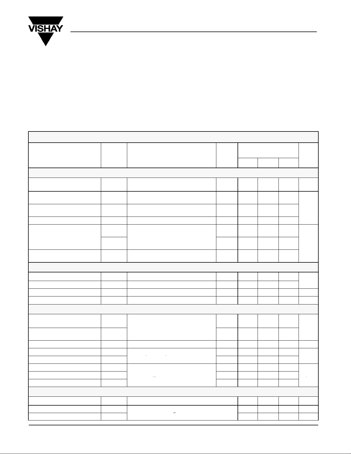
SPECIFICATIONS (V+ = 3.0 V)
Otherwise Unless Specified
Parameter Symbol
Analog Switch
Analog Signal Range
d
On-Resistance r
Flatness
Match
d
d
r
ON
r
ON
Switch Off Leakage Current
Channel-On Leakage Current I
VNO, VNC,
Flatness
rON Match V+ = 2.7 V, VD = 1.5 to V+, ID = 10 mA Room 0.3
I
I
COM(off)
COM(on)
V
COM
ON
rON
NO(off),
I
NC(off)
V+ = 3 V, "10%, VIN = 0.4 or 1.5 V
V+ = 2.7 V, V
V+ = 2.7 V, V
V
V+ = 3.3 V, V
New Product
Test Conditions
= 1.5 V, INO, INC = 10 mA
COM
= 1.5 to V+, INO, INC = 10 mA Room 0.5
COM
V+ = 3.3 V
VNC = 1 V/3 V, V
NO,
VNC = V
NO,
Vishay Siliconix
Power Dissipation (Packages)
c
MSOP-8
c
SOT23-8
Notes:
a. Signals on NC, NO, or COM or IN exceeding V+ will be clamped by
internal diodes. Limit forward diode current to maximum current ratings.
b. All leads welded or soldered to PC Board.
c. Derate 6.5 mW/_C above 25_C
e
= 3 V/1 V
COM
= 1 V/3 V
COM
b
Limits
-40 to 85_C
a
Temp
MinbTyp
Full 0 V+ V
Room
Full
Room
Full
Room
Full
Room
Full
-1
-10
-1
-10
-1
-10
c
MaxbUnit
3 6
7
1
10
1
10
1
10
320 mW. . . . . . . . . . . . . . . . . . . . . . . . . . . . . . . . . . . . . . . . . . . . . . . . . .
515 mW. . . . . . . . . . . . . . . . . . . . . . . . . . . . . . . . . . . . . . . . . . . . . . . . .
W
nA
Digital Control
Input High Voltage V
Input Low Voltage V
Input Capacitance
d
Input Current I
Dynamic Characteristics
Turn-On Time t
Turn-Off Time t
Charge Injection
Off-Isolation
Crosstalk
Source-Off Capacitance
Drain-Off Capacitance
Channel-On Capacitance
d
d
d
d
d
d
Power Supply
Power Supply Range V+ 2.7 3.3 V
Power Supply Current I+
Power Consumption P
Document Number: 72359
S-31642—Rev. A, 01-Aug-03
INH
INL
C
or I
INL
ON
OFF
Q
OIRR
X
TALK
C
NC/NO(off)
C
COM(off)
C
ON
INJ
Full 1.5
Full 0.4
in
INH
VNO or VNC = 2.0 V, RL = 300 W, CL = 35 pF
CL = 1 nF, V
RL = 50 W, CL = 5 pF, f = 1 MHz
f = 1 MHz Full 8 pF
VIN = 0 or V+ Full -1 1
Figure 1 and 2
= 0 V, R
GEN
= 0 W, Figure 3
GEN
Room
Full
Room
Full
Room 1 pC
22 35
40
17 31
35
Room -61
Room -67
V
mA
ns
dB
Room 17
VIN = 0 or V+, f = 1 MHz
Room 19
pF
Room 35
C
VIN = 0 or V+
0.02 1.0
3.3
mA
mW
www.vishay.com
3

DG2037/2038/2039
f
V+ = 5.5 V
VNO or VNC = 3 V, RL = 300 W, CL = 35 pF
IN
p
Vishay Siliconix
New Product
SPECIFICATIONS (V+ = 5.0 V)
Test Conditions
Otherwise Unless Specified
Parameter Symbol
V+ = 5 V, "10%, VIN = 0.8 or 2.4 V
e
Temp
a
Min
Analog Switch
Analog Signal Range
d
On-Resistance r
Flatness
Match
d
d
r
ON
r
ON
Switch Off Leakage Current
Channel-On Leakage Current
f
VNO, VNC,
V
COM
ON
r
ON
Flatness
V+ = 4.5 V, V
V+ = 4.5 V, V
= 2.5 V, INO, INC = 10 mA
COM
= 2.5 to V+, INO, INC = 10 mA Room 0.4
COM
rON Match V+ = 4.5 V, ID = 10 mA, V
I
NO(off),
I
NC(off)
I
COM(off)
I
COM(on)
V
NO,
V
V+ = 5.5 V
VNC = 1 V/4.5 V, V
V+ = 5.5 V
VNC = V
NO,
COM
COM
= 1 V/4.5 V
Full 0 V+ V
Room
Full
= 2.5 V Room 0.2
COM
Room
Full
= 4.5 V/1 V
Room
Full
Room
Full
Digital Control
Input High Voltage V
Input Low Voltage V
Input Capacitance C
Input Current I
INL
INH
INL
or I
in
INH
f = 1 MHz Full 8 pF
VIN = 0 or V+ Full -1 1
Full 2.4
Full 0.8
Dynamic Characteristics
Turn-On Time
Turn-Off Time
Charge Injection
Off-Isolation
Crosstalk
d
d
d
d
d
Source-Off Capacitance
Drain-Off Capacitance
d
Channel-On Capacitance
t
ON
t
OFF
Q
INJ
OIRR
X
d
d
TALK
C
NC/NO(off)
C
COM(off)
C
ON
VNO or VNC = 3 V, RL = 300 W, CL = 35 pF
Figure 1 and 2
CL = 1 nF, V
GEN
= 0 V, R
= 0 W, Figure 3
GEN
RL = 50 W, CL = 5 pF, f = 1 MHz
VIN = 0 or V+, f = 1 MHz
Room
Full
Room
Full
Room 1 pC
Room -61
Room -67
Room 15
Room 17
Room 35
Power Supply
Power Supply Range V+ 4.5 5.5 V
Power Supply Current I+
Power Consumption P
C
Notes:
a. Room = 25°C, Full = as determined by the operating suffix.
b. The algebraic convention whereby the most negative value is a minimum and the most positive a maximum, is used in this data sheet.
c. Typical values are for design aid only, not guaranteed nor subject to production testing.
d. Guarantee by design, nor subjected to production test.
= input voltage to perform proper function.
e. V
IN
f. Not production tested.
VIN = 0 or V+
-1
-10
-1
10
-1
-10
-40 to 85_C
b
Limits
c
Typ
2.5
1.6
19 30
12 22
0.02 1.0
MaxbUnit
5
6
1
10
1
10
1
10
35
30
5.5
W
nA
V
mA
ns
dB
pF
mA
mW
www.vishay.com
4
Document Number: 72359
S-31642—Rev. A, 01-Aug-03

DG2037/2038/2039
New Product
TYPICAL CHARACTERISTICS (25_C UNLESS NOTED)
8
7
W )
6
5
4
3
- On-Resistance (
ON
r
2
1
0
012345
10,000
1000
V+ = 5 V
V
rON vs. V
V
COM
Supply Current vs. Temperature
= 0 V
IN
Supply Voltage
COM
V+ = 1.8 V
V+ = 2.7 V
- Analog Voltage (V)
V+ = 3.3 V
V+ = 5.5 V
W )
- On-Resistance (
ON
r
100 mA
Vishay Siliconix
rON vs. Analog Voltage and Temperature
4.0
3.5
3.0
2.5
2.0
1.5
1.0
0.5
0123456
Supply Current vs. Input Switching Frequency
10 mA
1 mA
V+ = 5 V
V+ = 2.7 V
85_C
25_C
-40_C
V
- Analog Voltage (V)
COM
V+ = 5.5 V
85_C
25_C
-40_C
100
I+ - Supply Current (nA)
10
1
-40 -20 0 20 40 60 80 100
Temperature (_C)
Leakage Current vs. Temperature Leakage vs. Analog Voltage
1000
V+ = 5.5 V
100
I
COM(off)
I
10
Leakage Current (pA)
I
COM(on)
NO(off)
100 mA
10 mA
I+ - Supply Current (A)
1 mA
100 nA
10 nA
10 10 K 100 K100 1 K 1 M
150
100
I
NC(off)
50
0
-50
Leakage Current (pA)
-100
Input Switching Frequency (Hz)
V+ = 3.3 V
T = 25_C
I
COM(on)
I
COM(off)
10 M
1
-50 -25 0 25 50 75 100
Document Number: 72359
S-31642—Rev. A, 01-Aug-03
Temperature (_C)
-150
0.0 0.5 1.0 1.5 2.0 2.5 3.0
V
- Analog Voltage
COM
www.vishay.com
5

DG2037/2038/2039
Vishay Siliconix
New Product
TYPICAL CHARACTERISTICS (25_C UNLESS NOTED)
Switching Time vs. Temperature and Supply Voltage
30
25
t
V+ = 3.3 V
ON,
20
t
V+ = 5.5 V
- Switching Time (ns)
OFF
t
,
ON
t
ON,
15
10
5
0
-60 -40 -20 0 20 40 60 80 100 120 140
Temperature (_C)
t
OFF,
t
OFF,
V+ = 3.3 V
V+ = 5.5 V
Insertion Loss, Off-Isolation, Crosstalk vs. Frequency
10
OIRR
LOSS
X
TALK
X
, V+ = 5.5 V
TALK
10 K 1 M100 K1 K100
Frequency (Hz)
, V+ = 3.3 V
RL = 50 W
v+ = 5 v
v+ = 3 v
-10
(dB)
-30
TALK
-50
Loss, OIRR, X
-70
-110
2.0
1.8
1.6
1.4
1.2
1.0
0.8
- Switching Threshold (V)
0.6
T
V
0.4
0.2
0.0
0123456
Switching Threshold vs. Supply Voltage
V+ - Supply Voltage (V)
Charge Injection vs. Analog Voltage
12
10
Q @ Source
8
6
4
2
0
Q - Charge Injection (pC)
-2
V+ = 1.8 V
-4
-6
0123456
V+ = 3 V
V
- Analog Voltage (v)
COM
V+ = 5.5 V
www.vishay.com
6
Document Number: 72359
S-31642—Rev. A, 01-Aug-03

DG2037/2038/2039
TEST CIRCUITS
NO or NC
IN
GND
CL (includes fixture and stray capacitance)
V
OUT
Logic
Input
Switch
Input
V+
V+
+ V
COM
COM
ǒ
RL) R
Switch Output
R
L
300 W
R
L
Ǔ
ON
New Product
Logic
Input
V
OUT
Switch
C
L
35 pF
FIGURE 1. Switching Time
Output
Vishay Siliconix
V
INH
V
INL
0 V
t
ON
Logic “1” = Switch On
Logic input waveforms inverted for switches that have
the opposite logic sense.
50%
tr t 5 ns
t 5 ns
t
f
0.9 x V
t
OFF
OUT
V
gen
VIN = 0 - V+
Analyzer
V+
R
gen
+
COM
IN
V+
GND
NC or NO
C
V
= 1 nF
L
OUT
V
OUT
IN
IN depends on switch configuration: input polarity
determined by sense of switch.
DV
OUT
Q = DV
Off
OUT
x C
OnOn
L
FIGURE 2. Charge Injection
V+
10 nF
V+
NC or NO
IN
COM
R
L
GND
Off Isolation + 20 log
0 V, 2.4 V
V
V
NOńNC
0 V, 2.4 V
COM
10 nF
V+
V+
COM
Meter
IN
NC or NO
GND
HP4192A
Impedance
Analyzer
or Equivalent
f = 1 MHz
Document Number: 72359
S-31642—Rev. A, 01-Aug-03
FIGURE 3. Off-Isolation FIGURE 4. Channel Off/On Capacitance
www.vishay.com
7
 Loading...