

Page 1
g
查询BUD636A供应商
Silicon NPN High Voltage Switching Transistor
Features
D
Simple-sWitch-Off Transistor (SWOT)
D
HIGH SPEED technology
D
Planar passivation
D
100 kHz switching rate
D
Very low switching losses
Applications
Electronic lamp ballast circuits
Switch-mode power supplies
D
Very low dynamic saturation
D
Very low operating temperature
D
Optimized RBSOA
D
High reverse voltage
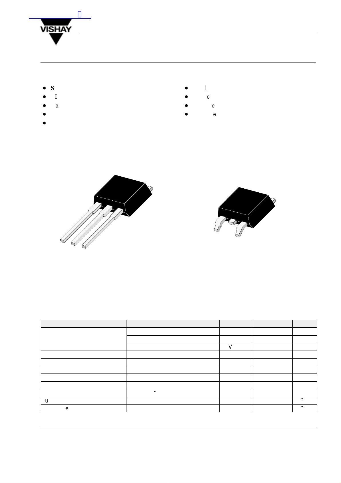
BUD636A
Vishay Telefunken
1
1
2
3
BUD636A
1 Base 2 Collector 3 Emitter
94 8964
BUD636A –SMD
1 Base 2 Collector 3 Emitter
Absolute Maximum Ratings
T
= 25°C, unless otherwise specified
case
Parameter Test Conditions Symbol Value Unit
Collector-emitter voltage V
V
Emitter-base voltage V
Collector current I
Collector peak current I
Base current I
Base peak current I
Total power dissipation T
Junction temperature T
Storage temperature range T
≤ 25°C P
case
V
3
CEO
CEW
CES
EBO
C
CM
B
BM
tot
j
stg
2
94 8965
450 V
550 V
1000 V
11 V
5 A
7.5 A
2.5 A
4 A
40 W
150
–65 to +150
°
C
°
C
Document Number 86504
Rev. 2, 20–Jan–99
www.vishay.de • FaxBack +1-408-970-5600
1 (9)
Page 2
BUD636A
g
g
yg
C B1
C B1
C B1 B2
C B1 B2
Vishay Telefunken
Maximum Thermal Resistance
T
= 25°C, unless otherwise specified
case
Parameter Test Conditions Symbol Value Unit
Junction case R
Electrical Characteristics
T
= 25°C, unless otherwise specified
case
Parameter Test Conditions Symbol Min Typ Max Unit
Collector cut-off current V
Collector-emitter breakdown
voltage (figure 1)
Emitter-base breakdown voltage IE = 1 mA V
Collector-emitter saturation voltage IC = 0.8 A; IB = 0.2 A V
Base-emitter saturation voltage IC = 0.8 A; IB = 0.2 A V
DC forward current transfer ratio VCE = 2 V; IC = 10 mA h
Collector-emitter working voltage VS = 50 V; L = 1 mH; IC = 5 A;
Dynamic saturation voltage IC = 2.5 A; IB = 0.5 A, t = 1 ms V
Gain bandwidth product IC = 200 mA; VCE = 10 V;
= 1000 V I
CES
V
= 1000 V; T
CES
IC = 300 mA; L = 125 mH;
I
measure
= 100 mA
= 150°C I
case
V
(BR)CEO
(BR)EBO
IC = 2.5 A; IB = 0.8 A V
IC = 2.5 A; IB = 0.8 A V
VCE = 2 V; IC = 0.8 A h
VCE = 2 V; IC = 2.5 A h
VCE = 5 V; IC = 5 A h
V
IB1 = 1.7 A; –IB2 = 0.5 A;
–VBB = 5 V
CEsatdyn
IC = 2.5 A; IB = 0.5 A; t = 3 ms V
CEsatdyn
f = 1 MHz
thJC
CES
CES
CEsat
CEsat
BEsat
BEsat
FE
FE
FE
FE
CEW
f
T
3.12 K/W
50
m
0.5 mA
450 V
11 V
0.1 0.2 V
0.2 0.4 V
0.9 1 V
1 1.2 V
15 22
15 21
7 10
4 6
550 V
10 15 V
2.8 5 V
4 MHz
A
Switching Characteristics
T
= 25°C, unless otherwise specified
case
Parameter Test Conditions Symbol Min Typ Max Unit
Resistive load (figure 2)
Turn on time IC = 0.8 A; IB1 = 0.2 A; t
Storage time
–IB2 = 0.4 A; VS = 250 V
Fall time t
Turn on time IC = 2.5 A; IB1 = 0.5 A; t
Storage time
–IB2 = 1.3 A; VS = 250 V
Fall time t
Inductive load (figure 3)
Storage time IC = 0.8 A; IB1 = 0.2 A; –IB2 = 0.4 A; t
V
Fall time
= 300 V; L = 200 mH
clamp
Storage time IC = 2.5 A; IB1 = 0.5 A; –IB2 = 1.3 A; t
V
Fall time
www.vishay.de • FaxBack +1-408-970-5600
2 (9)
= 300 V; L = 200 mH
clamp
on
t
on
t
t
t
s
f
s
f
s
f
s
f
0.15 0.25
3 3.5
0.3 0.45
0.4 0.6
1.3 1.5
0.1 0.15
3 3.5
0.2 0.3
1.4 1.7
0.1 0.15
Document Number 86504
Rev. 2, 20–Jan–99
m
s
m
s
m
s
m
s
m
s
m
s
m
s
m
s
m
s
m
s
Page 3
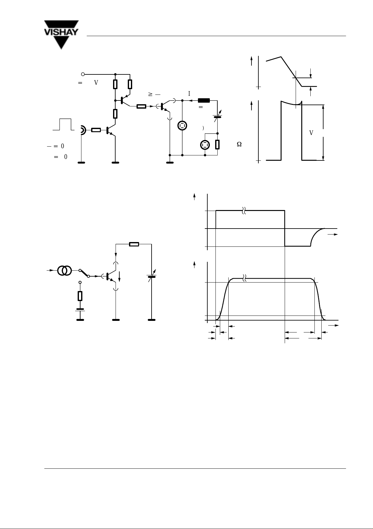
94 8863
3 Pulses
t
p
+
T
tp+
V
S2
0.1
10 ms
+
10 V
IBw
BUD636A
Vishay Telefunken
I
C
I
measure
I
C
5
ICL
C
VS1+
0to30V
V
(BR)CEO
I
(BR)R
+
100 m
V
CE
V
(BR)CEO
W
94 8852
I
B1
Figure 1. Test circuit for V
I
B
I
B1
(BR)CE0
0
t
–I
R
C
I
C
B2
(1)
I
V
I
B
R
B
V
BB
+
CE
V
CC
(1) Fast electronic switch
C
0.9 I
0.1 I
C
C
t
r
t
d
t
on
t
s
t
off
t
t
f
Document Number 86504
Rev. 2, 20–Jan–99
Figure 2. Test circuit for switching characteristics – resistive load
www.vishay.de • FaxBack +1-408-970-5600
3 (9)
Page 4

BUD636A
Vishay Telefunken
94 8853
I
B
I
B1
–I
0.9 I
0.1 I
0
t
B2
I
C
C
C
L
C
(2)
I
C
(1)
I
B1
V
BB
I
B
R
B
+
V
CE
V
clamp
V
CC
t
(1) Fast electronic switch
t
r
s
t
(2) Fast recovery rectifier
Figure 3. Test circuit for switching characteristics – inductive load
www.vishay.de • FaxBack +1-408-970-5600
4 (9)
Document Number 86504
Rev. 2, 20–Jan–99
Page 5
BUD636A
Vishay Telefunken
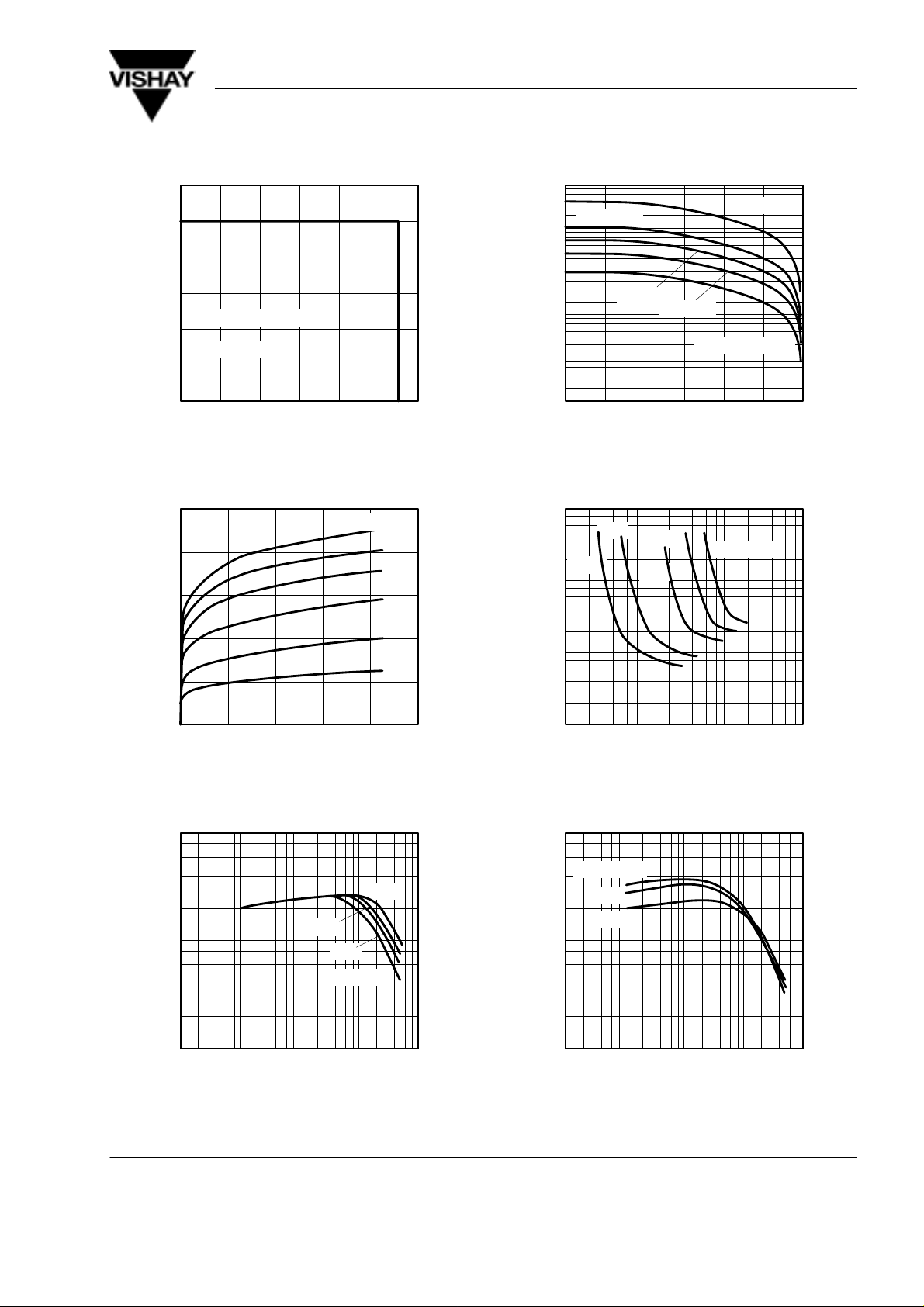
Typical Characteristics (T
6
5
4
3
C
CEsat
< I
< 2V
< 0.5 x I
B2
CEW
C
– Diagram
IB = 490 mA
C
I – Collector Current ( A )
95 10508
0.1 x I
2
V
1
0
0 100 200 300 400
VCE – Collector Emitter Voltage ( V )
Figure 4. V
5
4
3
= 25_C unless otherwise specified)
case
100
12.5 K/W
10
1
25 K/W
0.1
0.01
tot
P – Total Power Dissipation ( W )
0.001
95 10499
0 25 50 75 100
T
– Case Temperature ( °C )
case
500
600
Figure 7. P
10
0.6A
1A
2A
400 mA
290 mA
190 mA
1
50 K/W
vs.T
tot
3A
R
thJA
case
IC = 4A
3.12 K/W
= 135 K/W
125
150
2
C
I – Collector Current ( A )
1
0
04 81216
95 10512
VCE – Collector Emitter Voltage ( V )
Figure 5. IC vs. V
100
10
FE
h – Forward DC Current Transfer Ratio
1
0.001 0.01 0.1 1
95 10510
IC – Collector Current ( A )
10V
CE
5V
VCE = 2V
95 mA
49 mA
25V
0.1
20
10
0.01
0.01 0.1 1
CEsat
V – Collector Emitter Saturation Voltage ( V )
95 10513
IB – Base Current ( A )
Figure 8. V
100
Tj = 125°C
75°C
25°C
10
FE
h – Forward DC Current Transfer Ratio
1
0.001 0.01 0.1 1
95 10511
IC – Collector Current ( A )
CEsat
vs. I
10
B
10
Figure 6. hFE vs. I
Document Number 86504
Rev. 2, 20–Jan–99
C
Figure 9. hFE vs. I
www.vishay.de • FaxBack +1-408-970-5600
C
5 (9)
Page 6

BUD636A
Vishay Telefunken
10
8
m
6
T
= 125°C
case
4
s
t – Storage Time ( s )
2
0
25°C
02468
95 10517 –I
Figure 10. ts vs. –IB2/I
10
8
m
6
4
s
t – Storage Time ( s )
2
0
0 0.8 1.6 2.4 3.2
95 10515
saturated switching
R–load
I
= 0.8A, I
C
B2/IB1
B1
B1
saturated switching
R–load
I
= 0.8A, I
C
T
case
B1
= 125°C
25°C
–I
B2/IB1
= 0.1A
= 0.2A
10
4.0
1.0
0.8
m
0.6
T
= 125°C
case
0.4
f
t – Fall Time ( s )
0.2
0
02468
95 10516 –I
Figure 12. tf vs. –IB2/I
1.0
0.8
m
0.6
T
= 125°C
case
0.4
f
t – Fall Time ( s )
0.2
0
0 0.8 1.6 2.4 3.2
95 10514
saturated switching
R–load
I
= 0.8A, I
C
B1
25°C
B2/IB1
B1
saturated switching
R–load
I
= 0.8A, I
C
B1
25°C
–IB2/I
B1
= 0.1A
= 0.2A
10
4.0
Figure 11. ts vs. –IB2/I
www.vishay.de • FaxBack +1-408-970-5600
6 (9)
B1
Figure 13. tf vs. –IB2/I
Document Number 86504
B1
Rev. 2, 20–Jan–99
Page 7
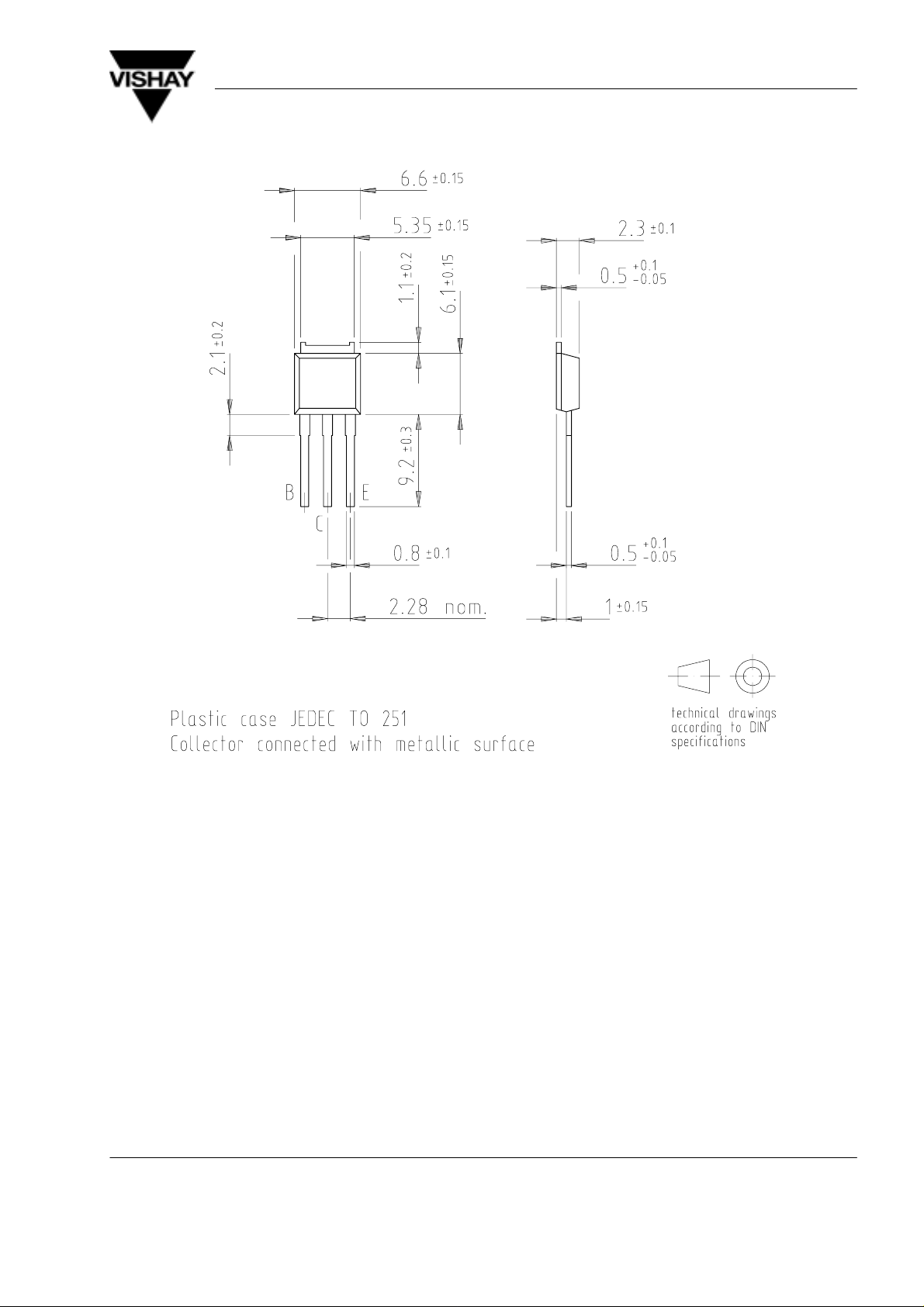
Dimensions in mm
BUD636A
Vishay Telefunken
Document Number 86504
Rev. 2, 20–Jan–99
14292
www.vishay.de • FaxBack +1-408-970-5600
7 (9)
Page 8

BUD636A
Vishay Telefunken
For ordering TO 252 add SMD to the type number (i.e. BUD636A –SMD)
www.vishay.de • FaxBack +1-408-970-5600
8 (9)
14293
Document Number 86504
Rev. 2, 20–Jan–99
Page 9

BUD636A
Vishay Telefunken
Ozone Depleting Substances Policy Statement
It is the policy of Vishay Semiconductor GmbH to
1. Meet all present and future national and international statutory requirements.
2. Regularly and continuously improve the performance of our products, processes, distribution and operating
systems with respect to their impact on the health and safety of our employees and the public, as well as their
impact on the environment.
It is particular concern to control or eliminate releases of those substances into the atmosphere which are known as
ozone depleting substances (ODSs).
The Montreal Protocol (1987) and its London Amendments (1990) intend to severely restrict the use of ODSs and
forbid their use within the next ten years. V arious national and international initiatives are pressing for an earlier ban
on these substances.
Vishay Semiconductor GmbH has been able to use its policy of continuous improvements to eliminate the use of
ODSs listed in the following documents.
1. Annex A, B and list of transitional substances of the Montreal Protocol and the London Amendments respectively
2. Class I and II ozone depleting substances in the Clean Air Act Amendments of 1990 by the Environmental
Protection Agency (EPA) in the USA
3. Council Decision 88/540/EEC and 91/690/EEC Annex A, B and C (transitional substances) respectively.
Vishay Semiconductor GmbH can certify that our semiconductors are not manufactured with ozone depleting
substances and do not contain such substances.
We reserve the right to make changes to improve technical design and may do so without further notice.
Parameters can vary in different applications. All operating parameters must be validated for each customer application
by the customer. Should the buyer use Vishay-Telefunken products for any unintended or unauthorized application, the
buyer shall indemnify Vishay-Telefunken against all claims, costs, damages, and expenses, arising out of, directly or
indirectly , any claim of personal damage, injury or death associated with such unintended or unauthorized use.
Document Number 86504
Rev. 2, 20–Jan–99
Vishay Semiconductor GmbH, P.O.B. 3535, D-74025 Heilbronn, Germany
Telephone: 49 (0)7131 67 2831, Fax number: 49 (0)7131 67 2423
www.vishay.de • FaxBack +1-408-970-5600
9 (9)
 Loading...