

Page 1
Silicon PIN Photodiode
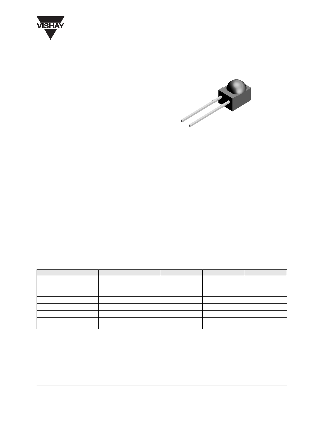
Description
BPV22NF(L) is a high speed and high sensitive PIN
photodiode in a plastic package with a spherical side
view lens.
The epoxy package itself is an IR filter, spectrally
matched to GaAs on GaAs and GaAlAs on GaAlAs IR
emitters (λ
Lens radius and chip position are perfectly matched
to the chip size, giving high sensitivity without compromising the viewing angle.
In comparison with flat packages the spherical lens
package achieves a sensitivity improvement of 80 %.
= 950 nm, s
p
(λ = 875 nm) > 90 %).
rel
BPV22NF(L)
Vishay Semiconductors
94 8633
Features
• Large radiant sensitive area (A = 7.5 mm2)
• Wide viewing angle ϕ = ± 60 °
• Improved sensitivity
• Fast response times
• Low junction capacitance
• Plastic package with universal IR filter
Applications
Infrared remote control and free air transmission systems in combination with IR emitter diodes (TSU.-,
TSI.-, or TSH.-Series). High sensitivity detector for
high data rate transmission systems.
The IR filter matches perfectly to the high speed infrared emitters in the 830 nm to 880 nm wavelength
range.
• Option "L": long lead package optional available
with suffix "L"; e.g.: BPV23FL
• Lead-free component
• Component in accordance to RoHS 2002/95/EC
and WEEE 2002/96/EC
Absolute Maximum Ratings
T
= 25 °C, unless otherwise specified
amb
Parameter Test condition Symbol Val ue Unit
Reverse Voltage V
Power Dissipation T
Junction Temperature T
Operating Temperature Range T
Storage Temperature Range T
Soldering Temperature t ≤ 5 s T
Thermal Resistance Junction/
Ambient
≤ 25 °C P
amb
R
V
j
amb
stg
sd
R
thJA
60 V
215 mW
100 °C
- 55 to + 100 °C
- 55 to + 100 °C
260 °C
350 K/W
Document Number 81509
Rev. 1.4, 08-Mar-05
www.vishay.com
1
Page 2

BPV22NF(L)
Vishay Semiconductors
Electrical Characteristics
T
= 25 °C, unless otherwise specified
amb
Parame te r Test condition Symbol Min Ty p. Max Unit
Forward Voltage I
Breakdown Voltage I
Reverse Dark Current V
Diode capacitance V
Serial Resistance V
= 50 mA V
F
= 100 µA, E = 0 V
R
= 10 V, E = 0 I
R
= 0 V, f = 1 MHz, E = 0 C
R
= 12 V, f = 1 MHz R
R
F
(BR)
ro
D
S
60 V
Optical Characteristics
T
= 25 °C, unless otherwise specified
amb
Parame te r Test condition Symbol Min Ty p. Max Unit
TK
TK
V
o
Vo
I
k
I
ra
Ira
p
0.5
*
D
r
f
c
c
55 85 µA
Open Circuit Voltage
Temp. Coefficient of V
o
Short Circuit Current
Reverse Light Current
Temp. Coefficient of I
ra
Absolute Spectral Sensitivity V
= 1 mW/cm2, λ = 950 nm
E
e
Ee = 1 mW/cm2, λ = 950 nm
= 1 mW/cm2, λ = 950 nm
E
e
= 1 mW/cm2, λ = 870 nm,
E
e
= 5 V
V
R
Ee = 1 mW/cm2, λ = 950 nm,
= 10 V
V
R
= 5 V, λ = 870 nm s(λ) 0.57 A/W
R
V
= 5 V, λ = 950 nm s(λ)0.6A/W
R
Angle of Half Sensitivity ϕ ± 60 deg
Wavelength of Peak Sensitivity λ
Range of Spectral Bandwidth λ
Quantum Efficiency λ = 950 nm η 90 %
Noise Equivalent Power V
Detectivity V
Rise Time V
Fall Time V
Cut-Off Frequency V
= 10 V, λ = 950 nm NEP
R
= 10 V, λ = 950 nm
R
= 10 V, RL = 1 kΩ, λ = 820 nm t
R
= 10 V, RL = 1 kΩ, λ = 820 nm t
R
= 12 V, RL = 1 kΩ, λ = 870 nm f
R
= 12 V, RL = 1 kΩ, λ = 950 nm f
V
R
11.3V
230nA
70 pF
400 Ω
370 mV
- 2.6 mV/K
80 µA
0.1 %/K
940 nm
790 to 1050 nm
4 x 10
6 x 10
-14
12
W/√ Hz
cm√Hz/W
100 ns
100 ns
4MHz
1MHz
www.vishay.com
2
Document Number 81509
Rev. 1.4, 08-Mar-05
Page 3
Vishay Semiconductors
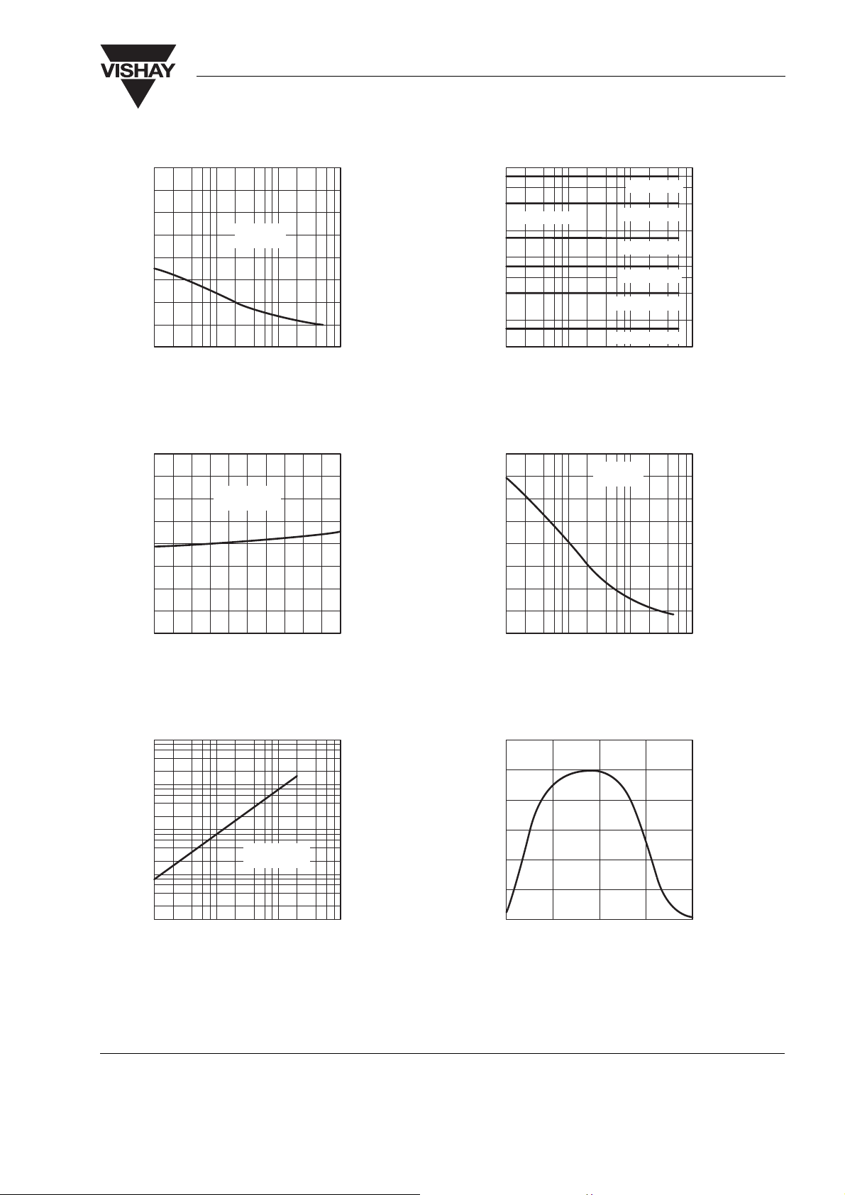
Typical Characteristics (Tamb = 25 °C unless otherwise specified)
BPV22NF(L)
8
6
E=0
f=1MHz
4
2
D
C - Diode Capacitance ( pF )
0
0.1 1 10
94 8430
VR- Reverse Voltage ( V )
100
Figure 1. Reverse Dark Current vs. Ambient Temperature
1.4
1.2
1.0
VR=5V
λ = 950 nm
100
2
2
2
2
2
2
100
µ
λ = 950 nm
10
ra
I - Reverse Light Current ( A )
1
0.1 1 10
94 8412
V
1 mW/cm
0.5 mW/cm
0.2 mW/cm
0.1 mW/cm
0.05 mW/cm
0.02 mW/cm
- Reverse Voltage ( V )
R
Figure 4. Reverse Light Current vs. Reverse Voltage
80
E=0
f=1MHz
60
40
0.8
ra rel
I - Relative Reverse Light Current
0.6
100806040200
T
94 8409
- Ambient Temperature ( ° C)
amb
Figure 2. Relative Reverse Light Current vs. Ambient Temperature
1000
µ
100
10
VR=5V
1
ra
I - Reverse Light Current ( A )
0.1
0.01 0.1 1
94 8411
Ee- Irradiance ( mW/cm2)
λ = 950 nm
10
Figure 3. Reverse Light Current vs. Irradiance
20
D
C - Diode Capacitance ( pF )
0
0.1 1 10
94 8407
VR- Reverse V oltage ( V )
100
Figure 5. Diode Capacitance vs. Reverse Voltage
1.2
1.0
0.8
0.6
0.4
0.2
rel
0.0
S(λ ) - Relative Spectral Sensitivity
750 850 950 1050 1150
94 8426
λ - Wavelength ( nm )
Figure 6. Relative Spectral Sensitivity vs. Wavelength
Document Number 81509
Rev. 1.4, 08-Mar-05
www.vishay.com
3
Page 4

BPV22NF(L)
Vishay Semiconductors
0°°°
10 20
1.0
0.9
0.8
rel
S - Relative Sensitivity
0.7
0.4 0.2 0 0.2 0.4
0.6
94 8413
Package Dimensions in mm
Figure 7. Relative Radiant Sensitivity vs. Angular Displacement
30°
40°
50°
60°
70°
80°
0.6
www.vishay.com
4
9612205
Document Number 81509
Rev. 1.4, 08-Mar-05
Page 5

Package Dimensions in mm
BPV22NF(L)
Vishay Semiconductors
95 11475
Document Number 81509
Rev. 1.4, 08-Mar-05
www.vishay.com
5
Page 6

BPV22NF(L)
Vishay Semiconductors
Ozone Depleting Substances Policy Statement
It is the policy of Vishay Semiconductor GmbH to
1. Meet all present and future national and international statutory requirements.
2. Regularly and continuously improve the performance of our products, processes, distribution and
operatingsystems with respect to their impact on the health and safety of our employees and the public, as
well as their impact on the environment.
It is particular concern to control or eliminate releases of those substances into the atmosphere which are
known as ozone depleting substances (ODSs).
The Montreal Protocol (1987) and its London Amendments (1990) intend to severely restrict the use of ODSs
and forbid their use within the next ten years. Various national and international initiatives are pressing for an
earlier ban on these substances.
Vishay Semiconductor GmbH has been able to use its policy of continuous improvements to eliminate the use
of ODSs listed in the following documents.
1. Annex A, B and list of transitional substances of the Montreal Protocol and the London Amendments
respectively
2. Class I and II ozone depleting substances in the Clean Air Act Amendments of 1990 by the Environmental
Protection Agency (EPA) in the USA
3. Council Decision 88/540/EEC and 91/690/EEC Annex A, B and C (transitional substances) respectively.
Vishay Semiconductor GmbH can certify that our semiconductors are not manufactured with ozone depleting
substances and do not contain such substances.
We reserve the right to make changes to improve technical design
and may do so without further notice.
Parameters can vary in different applications. All operating parameters must be validated for each
customer application by the customer. Should the buyer use Vishay Semiconductors products for any
unintended or unauthorized application, the buyer shall indemnify Vishay Semiconductors against all
claims, costs, damages, and expenses, arising out of, directly or indirectly, any claim of personal
damage, injury or death associated with such unintended or unauthorized use.
Vishay Semiconductor GmbH, P.O.B. 3535, D-74025 Heilbronn, Germany
Telephone: 49 (0)7131 67 2831, Fax number: 49 (0)7131 67 2423
www.vishay.com
6
Document Number 81509
Rev. 1.4, 08-Mar-05
Page 7

Legal Disclaimer Notice
Vishay
Document Number: 91000 www.vishay.com
Revision: 08-Apr-05 1
Notice
Specifications of the products displayed herein are subject to change without notice. Vishay Intertechnology, Inc.,
or anyone on its behalf, assumes no responsibility or liability for any errors or inaccuracies.
Information contained herein is intended to provide a product description only. No license, express or implied, by
estoppel or otherwise, to any intellectual property rights is granted by this document. Except as provided in Vishay's
terms and conditions of sale for such products, Vishay assumes no liability whatsoever, and disclaims any express
or implied warranty, relating to sale and/or use of Vishay products including liability or warranties relating to fitness
for a particular purpose, merchantability, or infringement of any patent, copyright, or other intellectual property right.
The products shown herein are not designed for use in medical, life-saving, or life-sustaining applications.
Customers using or selling these products for use in such applications do so at their own risk and agree to fully
indemnify Vishay for any damages resulting from such improper use or sale.
 Loading...