

Page 1
www.vishay.com
12785
Silicon NPN Phototransistor
DESCRIPTION
BPV11 is a silicon NPN phototransistor with high radiant
sensitivity in clear, T-1¾ plastic package with base terminal.
It is sensitive to visible and near infrared radiation.
BPV11
Vishay Semiconductors
FEATURES
• Package type: leaded
• Package form: T-1¾
• Dimensions (in mm): Ø 5
• High photo sensitivity
• High radiant sensitivity
• Suitable for visible and near infrared radiation
• Fast response times
• Angle of half sensitivity: = ± 15°
• Base terminal connected
• Material categorization: For definitions of compliance
please see www.vishay.com/doc?99912
APPLICATIONS
• Detector for industrial electronic circuitry, measurement
and control
PRODUCT SUMMARY
COMPONENT Ica (mA) (deg)
BPV11 10 ± 15 450 to 1080
Note
• Test condition see table “Basic Characteristics”
0.1
(nm)
ORDERING INFORMATION
ORDERING CODE PACKAGING REMARKS PACKAGE FORM
BPV11 Bulk MOQ: 4000 pcs, 4000 pcs/bulk T-1¾
Note
• MOQ: minimum order quantity
ABSOLUTE MAXIMUM RATINGS (T
PARAMETER TEST CONDITION SYMBOL VALUE UNIT
Collector base voltage V
Collector emitter voltage V
Emitter base voltage V
Collector current I
Collector peak current t
Power dissipation T
Junction temperature T
Operating temperature range T
Storage temperature range T
Soldering temperature t 5 s, 2 mm from body T
Thermal resistance junction/ambient Connected with Cu wire, 0.14 mm
= 25 °C, unless otherwise specified)
amb
/T = 0.5, tp 10 ms I
p
47 °C P
amb
2
R
CBO
CEO
EBO
C
CM
V
amb
stg
sd
thJA
80 V
70 V
5V
50 mA
100 mA
150 mW
j
100 °C
- 40 to + 100 °C
- 40 to + 100 °C
260 °C
350 K/W
Rev. 1.8, 03-May-13
For technical questions, contact: detectortechsupport@vishay.com
THIS DOCUMENT IS SUBJECT TO CHANGE WITHOUT NOTICE. THE PRODUCTS DESCRIBED HEREIN AND THIS DOCUMENT
ARE SUBJECT TO SPECIFIC DISCLAIMERS, SET FORTH AT www.vishay.com/doc?91000
1
Document Number: 81504
Page 2
www.vishay.com
94 8249
20
I
CEO
- Collector Dark Current (nA)
100
40 60 80
T
amb
- Ambient Temperature (°C)
10
10
1
10
2
10
3
10
4
VCE = 10 V
0
0.6
0.8
1.0
1.2
1.4
2.0
20 40 60 80
100
1.6
1.8
λ
94 8239
T
amb
- Ambient Temperature (°C)
I
ca rel
- Relative Collector Current
VCE = 5 V
E
e
= 1 mW/cm
2
= 950 nm
200
160
120
80
- Power Dissipation (mW)
40
V
P
BPV11
Vishay Semiconductors
R
thJA
0
100806040200
T
- Ambient Temperature (°C)
94 8300
amb
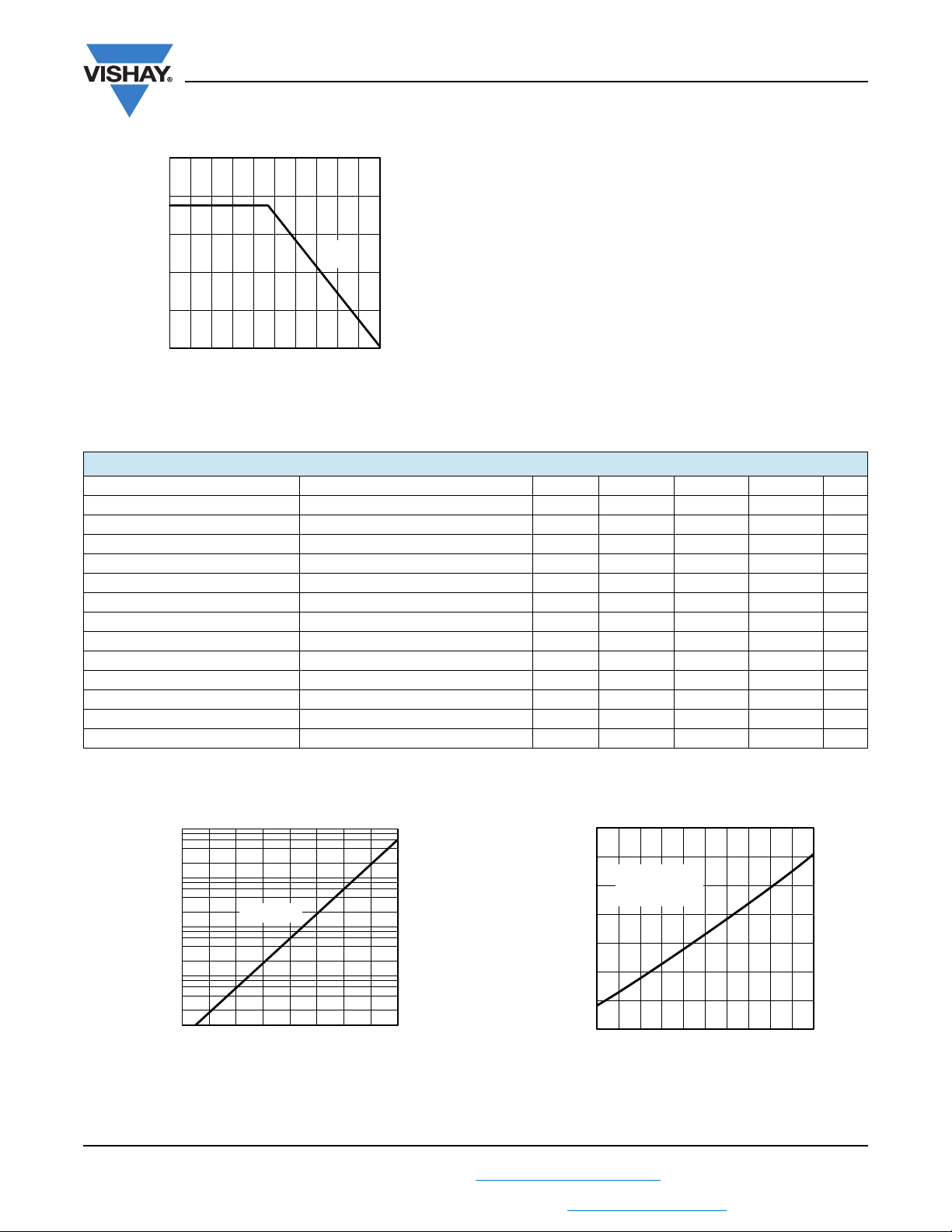
Fig. 1 - Power Dissipation Limit vs. Ambient Temperature
BASIC CHARACTERISTICS (T
= 25 °C, unless otherwise specified)
amb
PARAMETER TEST CONDITION SYMBOL MIN. TYP. MAX. UNIT
Collector emitter breakdown voltage I
Collector emitter dark current V
DC current gain V
Collector emitter capacitance V
Collector base capacitance V
Collector light current E
CE
CE
BE
= 1 mW/cm2, = 950 nm, VCE = 5 V I
e
= 1 mA V
C
= 10 V, E = 0 I
CE
= 5 V, IC = 5 mA, E = 0 h
= 0 V, f = 1 MHz, E = 0 C
= 0 V, f = 1 MHz, E = 0 C
(BR)CEO
CEO
FE
CEO
CBO
ca
70 V
150nA
450
15 pF
19 pF
310 mA
Angle of half sensitivity ± 15 deg
Wavelength of peak sensitivity
Range of spectral bandwidth
Collector emitter saturation voltage E
Turn-on time V
Turn-off time V
Cut-off frequency V
BASIC CHARACTERISTICS (T
= 1 mW/cm2, = 950 nm, IC = 1 mA V
e
= 5 V, IC = 5 mA, RL = 100 t
S
= 5 V, IC = 5 mA, RL = 100 t
S
= 5 V, IC = 5 mA, RL = 100 f
S
= 25 °C, unless otherwise specified)
amb
p
0.1
CEsat
on
off
c
850 nm
450 to 1080 nm
130 300 mV
6μs
5μs
110 kHz
Fig. 2 - Collector Dark Current vs. Ambient Temperature Fig. 3 - Relative Collector Current vs. Ambient Temperature
Rev. 1.8, 03-May-13
THIS DOCUMENT IS SUBJECT TO CHANGE WITHOUT NOTICE. THE PRODUCTS DESCRIBED HEREIN AND THIS DOCUMENT
2
Document Number: 81504
For technical questions, contact: detectortechsupport@vishay.com
ARE SUBJECT TO SPECIFIC DISCLAIMERS, SET FORTH AT www.vishay.com/doc?91000
Page 3

www.vishay.com
0.1 1 10
0.1
1
10
100
I
ca
- Collector Light Current (mA)
VCE - Collector Emitter Voltage (V)
100
94 8272
Ee = 1 mW/cm
2
λ = 950 nm
0.5 mW/cm
2
0.2 mW/cm
2
0.1 mW/cm
2
0.05 mW/cm
2
0.02 mW/cm
2
0.01 0.1 1 10
0
200
400
600
800
B - Amplification
IC - Collector Current (mA)
100
94 8250
VCE = 5 V
0.1 1 10
0
4
8
12
16
20
C
CBO
- Collector Base Capacitance (pF)
VCB - Collector Base Voltage (V)
100
94 8246
f = 1 MHz
100
10
1
0.1
- Collector Light Current (mA)
ca
I
0.01
0.01 0.1 1
94 8244
Ee - Irradiance (mW/cm²)
BPV11
Vishay Semiconductors
VCE = 5 V
λ = 950 nm
10
Fig. 4 - Collector Light Current vs. Irradiance
Fig. 5 - Collector Light Current vs. Collector Emitter Voltage
Fig. 7 - Collector Base Capacitance vs. Collector Base Voltage
20
16
12
8
4
f = 1 MHz
- Collector Ermitter Capacitance (pF)
0
CEO
C
0.1 1 10
94 8247
VCE - Collector Ermitter Voltage (V)
100
Fig. 8 - Collector Emitter Capacitance vs. Collector Emitter Voltage
12
10
8
VCE = 5 V
R
= 100 Ω
L
λ = 950 nm
Rev. 1.8, 03-May-13
Fig. 6 - Amplification vs. Collector Current
THIS DOCUMENT IS SUBJECT TO CHANGE WITHOUT NOTICE. THE PRODUCTS DESCRIBED HEREIN AND THIS DOCUMENT
6
4
- Turn-on/Turn-off Time (µs)
off
2
/t
on
t
0
3
94 8253
Fig. 9 - Turn-on/Turn-off Time vs. Collector Current
IC - Collector Current (mA)
For technical questions, contact: detectortechsupport@vishay.com
ARE SUBJECT TO SPECIFIC DISCLAIMERS, SET FORTH AT www.vishay.com/doc?91000
t
on
t
off
1612840
Document Number: 81504
Page 4

www.vishay.com
Chip position
0.8
+ 0.2
- 0.1
Issue:1; 01.07.96
± 0.15
Drawing-No.: 6.544-5188.01-4
specifications
according to DIN
technical drawings
0.5
Area not plane
± 0.15
± 0.3
± 0.5
5.75
± 0.15
0.5
E
B
5
± 0.3
+ 0.15
0.8
C
1.5
± 0.25
- 0.1
+ 0.2
0.8
- 0.1
+ 0.2
- 0.1
+ 0.2
1.27 nom.
2.54 nom.
12.3
(4.55)
7.6
35
< 0.7
8.6
R 2.
45 (sphere)
96 12200
1.0
BPV11
Vishay Semiconductors
0°
10° 20°
30°
0.8
0.6
1.0
0.9
0.4
- Relative Spectral Sensitivity
0.2
rel
S (λ)
0
400 600 1000
94 8348
λ - Wavelength (nm)
800
0.8
- Relative Sensitivity
rel
S
0.7
0.6
94 8248
0.20.4
0
Fig. 10 - Relative Spectral Sensitivity vs. Wavelength Fig. 11 - Relative Radiant Sensitivity vs. Angular Displacement
PACKAGE DIMENSIONS in millimeters
40°
50°
60°
70°
ϕ - Angular Displacement
80°
Rev. 1.8, 03-May-13
THIS DOCUMENT IS SUBJECT TO CHANGE WITHOUT NOTICE. THE PRODUCTS DESCRIBED HEREIN AND THIS DOCUMENT
4
For technical questions, contact: detectortechsupport@vishay.com
Document Number: 81504
ARE SUBJECT TO SPECIFIC DISCLAIMERS, SET FORTH AT www.vishay.com/doc?91000
Page 5

Legal Disclaimer Notice
www.vishay.com
Vishay
Disclaimer
ALL PRODUCT, PRODUCT SPECIFICATIONS AND DATA ARE SUBJECT TO CHANGE WITHOUT NOTICE TO IMPROVE
RELIABILITY, FUNCTION OR DESIGN OR OTHERWISE.
Vishay Intertechnology, Inc., its affiliates, agents, and employees, and all persons acting on its or their behalf (collectively,
“Vishay”), disclaim any and all liability for any errors, inaccuracies or incompleteness contained in any datasheet or in any other
disclosure relating to any product.
Vishay makes no warranty, representation or guarantee regarding the suitability of the products for any particular purpose or
the continuing production of any product. To the maximum extent permitted by applicable law, Vishay disclaims (i) any and all
liability arising out of the application or use of any product, (ii) any and all liability, including without limitation special,
consequential or incidental damages, and (iii) any and all implied warranties, including warranties of fitness for particular
purpose, non-infringement and merchantability.
Statements regarding the suitability of products for certain types of applications are based on Vishay’s knowledge of
typical requirements that are often placed on Vishay products in generic applications. Such statements are not binding
statements about the suitability of products for a particular application. It is the customer’s responsibility to validate that a
particular product with the properties described in the product specification is suitable for use in a particular application.
Parameters provided in datasheets and / or specifications may vary in different applications and performance may vary over
time. All operating parameters, including typical parameters, must be validated for each customer application by the customer’s
technical experts. Product specifications do not expand or otherwise modify Vishay’s terms and conditions of purchase,
including but not limited to the warranty expressed therein.
Except as expressly indicated in writing, Vishay products are not designed for use in medical, life-saving, or life-sustaining
applications or for any other application in which the failure of the Vishay product could result in personal injury or death.
Customers using or selling Vishay products not expressly indicated for use in such applications do so at their own risk.
Please contact authorized Vishay personnel to obtain written terms and conditions regarding products designed for
such applications.
No license, express or implied, by estoppel or otherwise, to any intellectual property rights is granted by this document
or by any conduct of Vishay. Product names and markings noted herein may be trademarks of their respective owners.
© 2017 VISHAY INTERTECHNOLOGY, INC. ALL RIGHTS RESERVED
Revision: 08-Feb-17
1
Document Number: 91000
 Loading...