

Vishay Semiconductors
N-Channel MOS-Fieldeffect Triode, Depletion Mode
BF543
Features
1
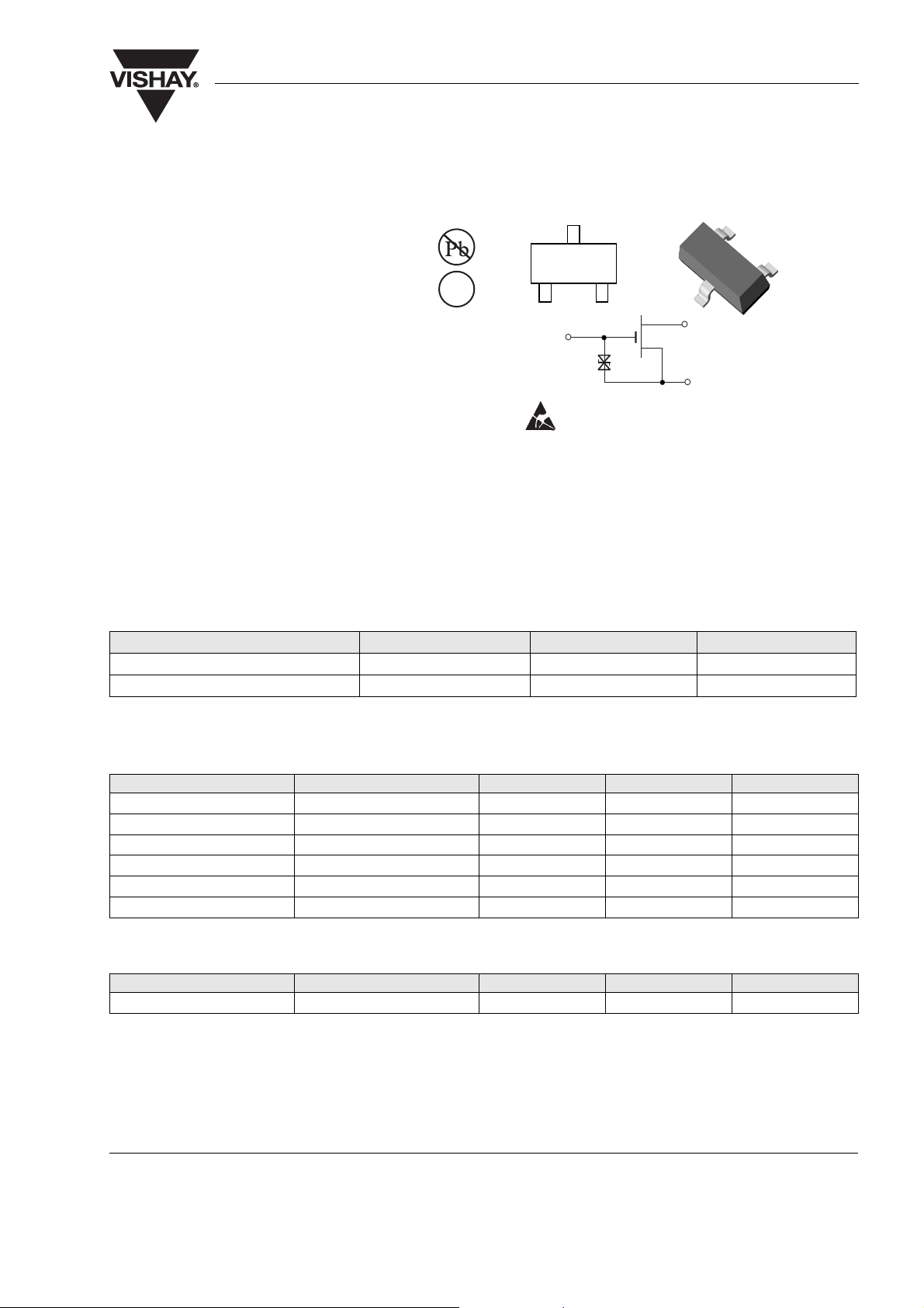
• Integrated gate protection diode
• Low feedback capacitance
• Low noise figure
• Lead (Pb)-free component
• Component in accordance to RoHS 2002/95/EC
e3
32
G
D
and WEEE 2002/96/EC
S
Applications
• High frequency stages up to 300 MHz
Electrostatic sensitive device.
Observe precautions for handling.
Mechanical Data
Case: SOT-23 Plastic case
Weight: approx. 8.0 mg
Pinning: 1 = Source, 2 = Gate, 3 = Drain
Parts Table
Part Ordering Code Type marking Remarks
BF543A BF543A-GS08 LD Tape and Reel
BF543B BF543B-GS08 LD Tape and Reel
19240
Absolute Maximum Ratings
T
= 25 °C, unless otherwise specified
amb
Parameter Test condition Symbol Val ue Unit
Drain - source voltage V
Drain current I
Gate - source peak current ± I
Total power dissipation T
Channel temperature T
Storage temperature range T
≤ 60 °C P
amb
Maximum Thermal Resistance
Parameter Test condition Symbol Val ue Unit
Channel ambient
1)
on glass fibre printed board (25 x 20 x 1.5) mm3 plated with 35 µm Cu
Document Number 85072
Rev. 1.6, 18-Jan-06
1)
R
DS
D
GSM
tot
Ch
stg
thChA
20 V
30 mA
10 mA
200 mW
150 °C
- 55 to +150 °C
450 K/W
www.vishay.com
1
BF543
Vishay Semiconductors
Electrical DC Characteristics
T
= 25 °C, unless otherwise specified
amb
Parameter Test condition Part Symbol Min Ty p. Max Unit
Drain - source breakdown
voltage
Gate - source breakdown
voltage
Gate - source leakage current ± V
Drain current V
Gate - source cut-off voltage V
Electrical AC Characteristics
T
= 25 °C, unless otherwise specified
amb
V
= 10 V, ID = 4 mA, f = 1 MHz
DS
Paramete r Test condition Symbol Min Ty p. Max Unit
Forward transadmittance |y
Gate 1 input capacitance C
Feedback capacitance C
Output capacitance C
Noise figure G
Power gain G
= 10 µA, - VGS = 4 V V
I
D
= 10 mA, VDS = 0 ± V
± I
GS
= 6 V, VDS = 0 ± I
GS
= 10 V, VGS = 0 I
DS
BF543A I
BF543B I
= 10 V, ID = 20 µA - V
DS
= 2 mS, GL = 0.5 mS,
S
f = 200 MHz
= 2 mS, GL = 0.5 mS,
S
f = 200 MHz
(BR)DS
(BR)GSS
GSS
DSS
DSS
DSS
GS(OFF)
|9.5 12 mS
21s
issg1
rss
oss
20 V
7.5 12 V
50 nA
1.5 8.0 mA
1.5 6.5 mA
4.0 8.0 mA
2.5 V
2.7 pF
25 fF
0.9 pF
F1.0dB
G
ps
22 dB
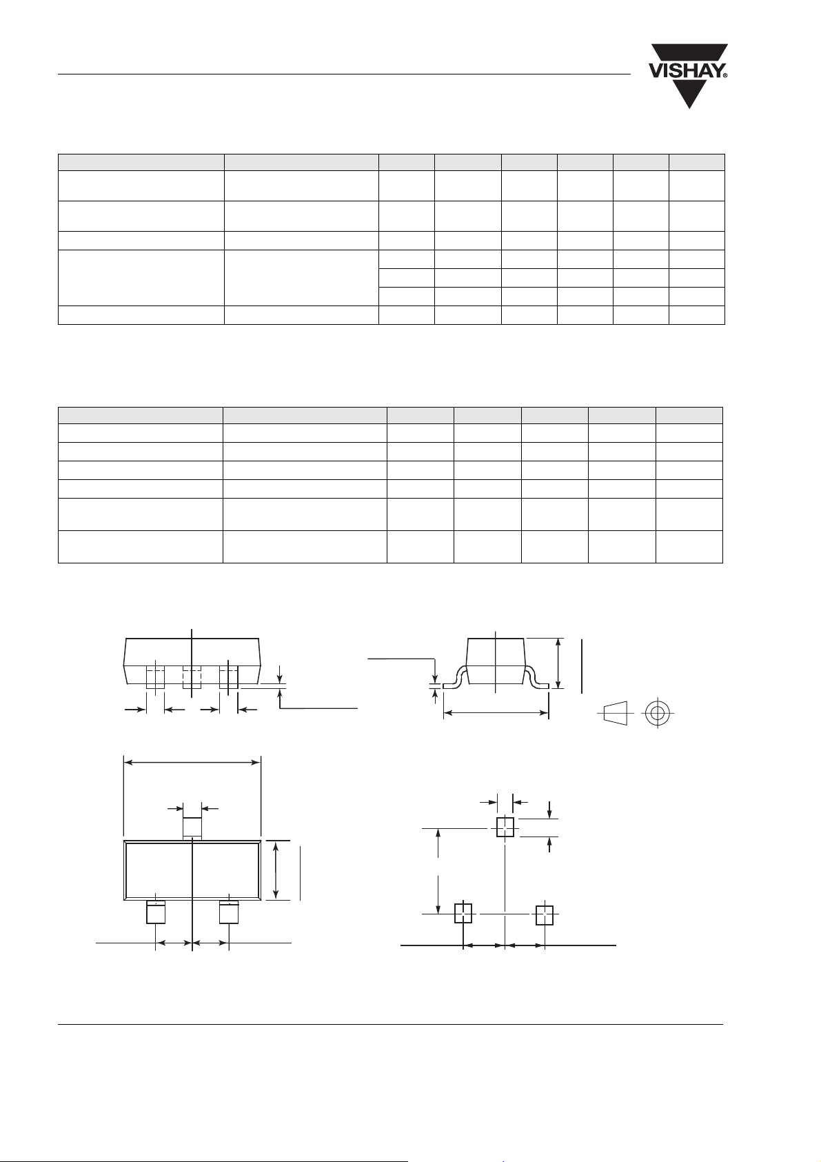
Package Dimensions in mm (Inches)
0.1 (.004) max.
0.4 (.016)0.4 (.016)
3.1 (.122)
2.8 (.110)
0.4 (.016)
1.20(.047)
1.43 (.056)
0.95 (.037)0.95 (.037)
0.175 (.007)
0.098 (.005)
2.0 (0.079)
2.6 (.102)
2.35 (.092)
Mounting Pad Layout
0.52 (0.020)
0.9 (0.035)
0.95 (0.037)0.95 (0.037)
1.15 (.045)
0.95 (.037)
ISO Method E
17418
www.vishay.com
2
Document Number 85072
Rev. 1.6, 18-Jan-06

BF543
Vishay Semiconductors
Ozone Depleting Substances Policy Statement
It is the policy of Vishay Semiconductor GmbH to
1. Meet all present and future national and international statutory requirements.
2. Regularly and continuously improve the performance of our products, processes, distribution and operating
systems with respect to their impact on the health and safety of our employees and the public, as well as
their impact on the environment.
It is particular concern to control or eliminate releases of those substances into the atmosphere which are
known as ozone depleting substances (ODSs).
The Montreal Protocol (1987) and its London Amendments (1990) intend to severely restrict the use of ODSs
and forbid their use within the next ten years. Various national and international initiatives are pressing for an
earlier ban on these substances.
Vishay Semiconductor GmbH has been able to use its policy of continuous improvements to eliminate the use
of ODSs listed in the following documents.
1. Annex A, B and list of transitional substances of the Montreal Protocol and the London Amendments
respectively
2. Class I and II ozone depleting substances in the Clean Air Act Amendments of 1990 by the Environmental
Protection Agency (EPA) in the USA
3. Council Decision 88/540/EEC and 91/690/EEC Annex A, B and C (transitional substances) respectively.
Vishay Semiconductor GmbH can certify that our semiconductors are not manufactured with ozone depleting
substances and do not contain such substances.
We reserve the right to make changes to improve technical design
and may do so without further notice.
Parameters can vary in different applications. All operating parameters must be validated for each
customer application by the customer. Should the buyer use Vishay Semiconductors products for any
unintended or unauthorized application, the buyer shall indemnify Vishay Semiconductors against all
claims, costs, damages, and expenses, arising out of, directly or indirectly, any claim of personal
damage, injury or death associated with such unintended or unauthorized use.
Vishay Semiconductor GmbH, P.O.B. 3535, D-74025 Heilbronn, Germany
Document Number 85072
Rev. 1.6, 18-Jan-06
www.vishay.com
3

 Loading...