

www.vishay.com
18109
12
3
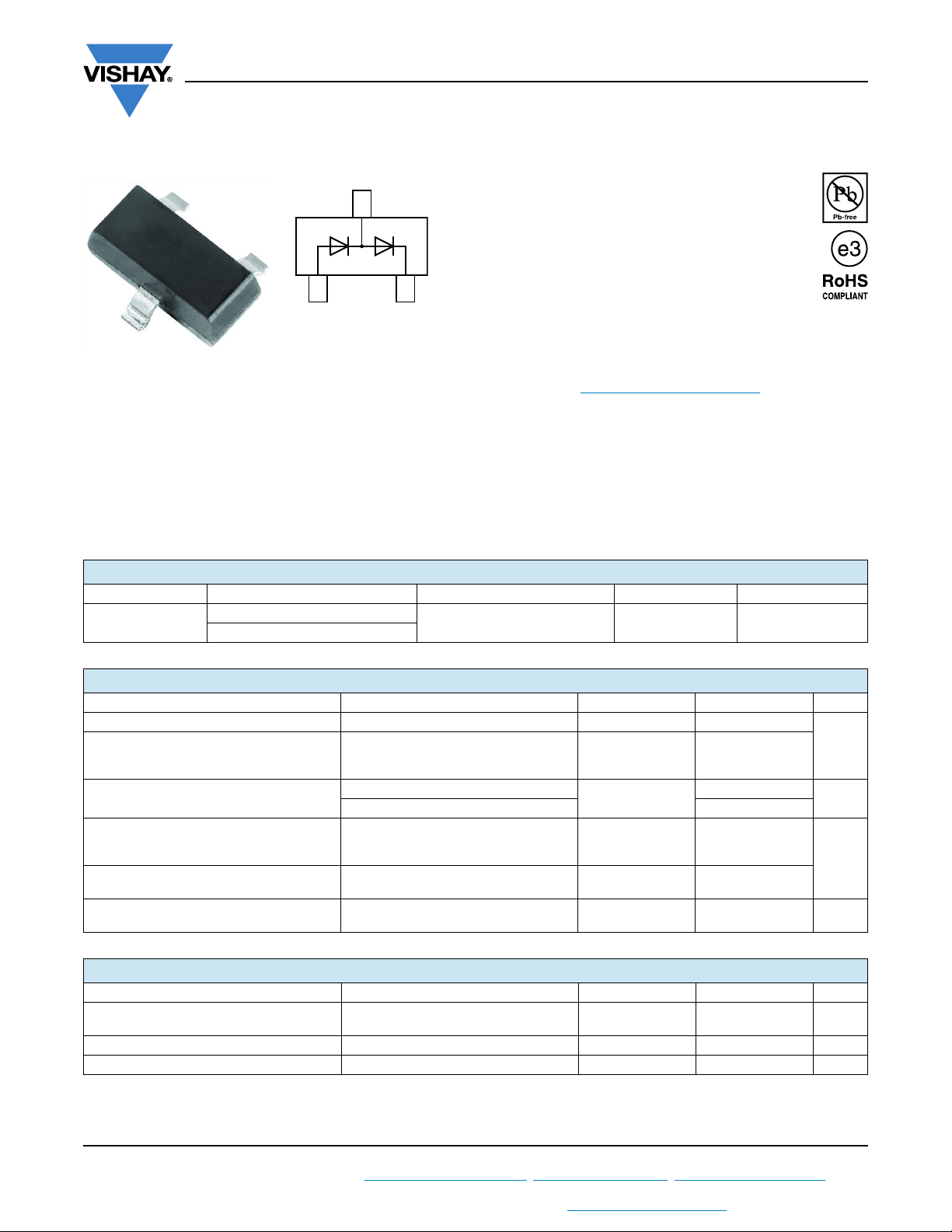
Small Signal Switching Diode, Dual in Series
MECHANICAL DATA
Case: SOT-23
Weight: approx. 8.8 mg
Packaging codes/options:
18/10K per 13" reel (8 mm tape), 10K/box
08/3K per 7" reel (8 mm tape), 15K/box
BAV99
Vishay Semiconductors
FEATURES
• Fast switching speed
• High conductance
• Surface mount package ideally suited for
automatic insertion
• Connected in series
• AEC-Q101 qualified
• Base P/N-E3 - RoHS-compliant, commercial grade
• Base P/N-HE3 - RoHS-compliant, AEC-Q101 qualified
• Material categorization: For definitions of compliance
please see www.vishay.com/doc?99912
PARTS TABLE
PART ORDERING CODE INTERNAL CONSTRUCTION TYPE MARKING REMARKS
BAV99
ABSOLUTE MAXIMUM RATINGS (T
PARAMETER TEST CONDITION SYMBOL VALUE UNIT
Non repetitive peak reverse voltage V
Repetitive peak reverse voltage
= working peak reverse voltage
= DC blocking voltage
Peak forward surge current
Average forward current
Forward current
Power dissipation
THERMAL CHARACTERISTICS (T
PARAMETER TEST CONDITION SYMBOL VALUE UNIT
Junction ambient
Junction and storage temperature range T
Operating temperature range T
BAV99-E3-08 or BAV99-E3-18
BAV99-HE3-08 or BAV99-HE3-18
= 25 °C, unless otherwise specified)
amb
Half wave rectification with resistive load
and f 50 MHz, on ceramic substrate
10 mm x 8 mm x 0.7 mm
10 mm x 8 mm x 0.7 mm
10 mm x 8 mm x 0.7 mm
= 25 °C, unless otherwise specified)
amb
10 mm x 8 mm x 0.7 mm
Dual diodes serial JE Tape and reel
RM
= V
V
RRM
RWM
t
= 1 s
p
= 1 μs 4.5
t
p
On ceramic substrate
On ceramic substrate
On ceramic substrate
I
FSM
I
F(AV)
P
R
= T
j
I
F
tot
thJA
op
stg
= V
100
R
70
1
150
250
300 mW
430 K/W
- 55 to + 150 °C
- 55 to + 150 °C
V
A
mA
Rev. 1.9, 16-May-13
For technical questions within your region: DiodesAmericas@vishay.com
THIS DOCUMENT IS SUBJECT TO CHANGE WITHOUT NOTICE. THE PRODUCTS DESCRIBED HEREIN AND THIS DOCUMENT
1
, DiodesAsia@vishay.com, DiodesEurope@vishay.com
ARE SUBJECT TO SPECIFIC DISCLAIMERS, SET FORTH AT www.vishay.com/doc?91000
Document Number: 85718
www.vishay.com
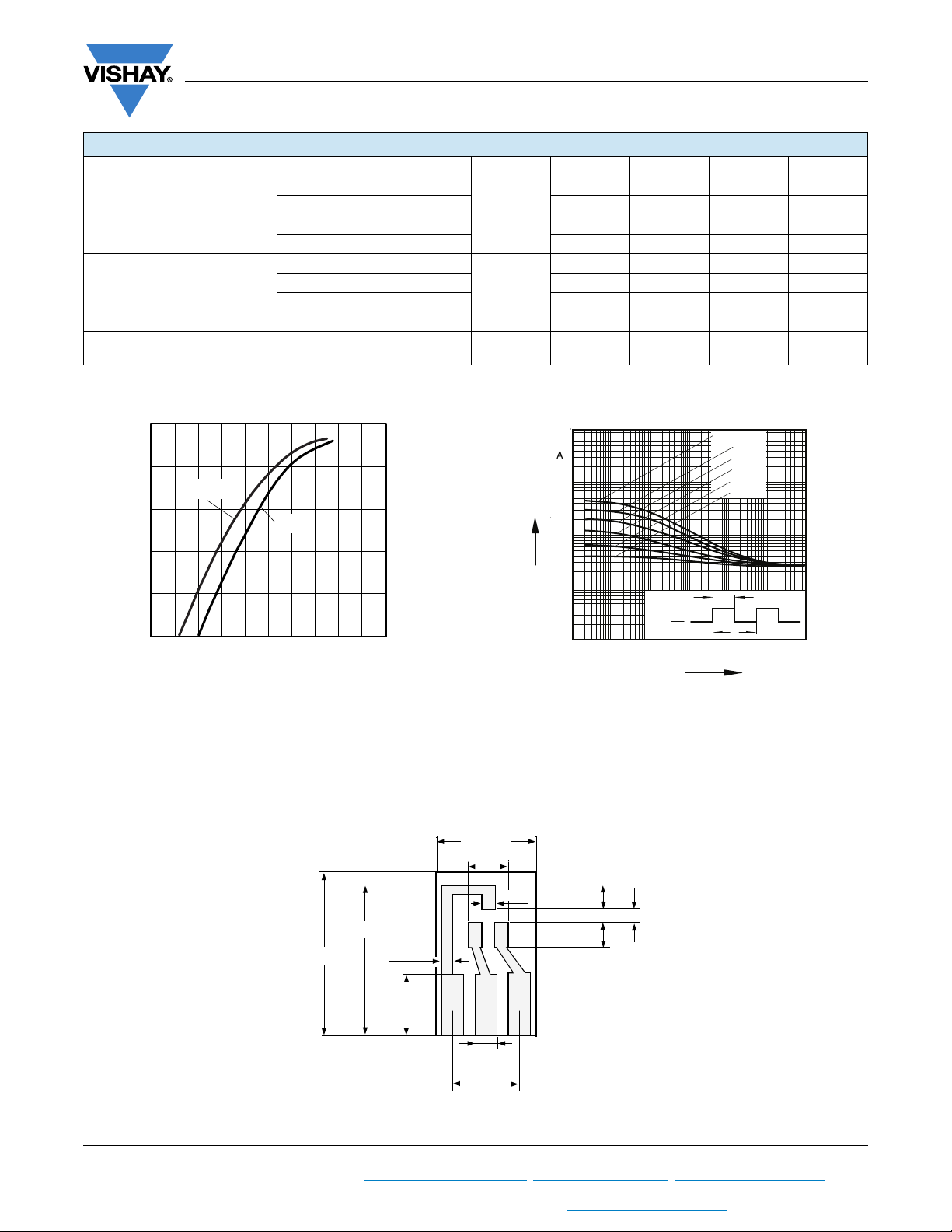
I - Forward Current (mA)
0.01
0.1
1
10
100
1000
0 0.2 0.4 0.6 0.8 1.0 1.2 1.4 1.6 1.8 2.0
V
F
-
Forward Voltage (V)
14356
F
Tj = 100 °C
25 °C
22290
10
2
10
1
10
-1
10
-2
10
-5
10
-6
10
-3
10
-4
10
-1
10
-2
10
-0
10
0
/
FM
t
s
D = 0.005
0.01
0.02
0.05
0.1
0.2
t
p
t
p
D =
T
T
17451
15 (0.59)
12 (0.47)
0.8 (0.03)
5 (0.2)
7.5 (0.3)
3 (0.12)
1 (0.4)
1 (0.4)
2 (0.8)
2 (0.8)
1.5 (0.06)
5.1 (0.2)
BAV99
Vishay Semiconductors
ELECTRICAL CHARACTERISTICS (T
= 25 °C, unless otherwise specified)
amb
PARAMETER TEST CONDITION SYMBOL MIN. TYP. MAX. UNIT
I
Forward voltage
Reverse current
V
V
Diode capacitance V
I
= 10 mA to iR = 1 mA,
Reverse recovery time
F
V
TYPICAL CHARACTERISTICS (T
= 1 mA
F
I
= 10 mA 0.855 V
F
I
= 50 mA 1 V
F
I
= 150 mA 1.25 V
F
V
= 70 V
R
= 70 V, Tj = 150 °C 50 μA
R
= 25 V, Tj = 150 °C 30 μA
R
= 0, f = 1 MHz C
R
= 6 V, RL = 100
R
= 25 °C, unless otherwise specified)
amb
V
F
I
R
D
t
rr
0.715 V
2500 nA
1.5 pF
6ns
Fig. 1 - Forward Current vs. Forward Voltage Fig. 2 - Peak forward current /
LAYOUT FOR R
thJA
TEST
Thickness:
Fiberglass 1.5 mm (0.059 inches)
Copper leads 0.3 mm (0.012 inches)
ARE SUBJECT TO SPECIFIC DISCLAIMERS, SET FORTH AT www.vishay.com/doc?91000
Rev. 1.9, 16-May-13
For technical questions within your region: DiodesAmericas@vishay.com
THIS DOCUMENT IS SUBJECT TO CHANGE WITHOUT NOTICE. THE PRODUCTS DESCRIBED HEREIN AND THIS DOCUMENT
= f (t
FM
2
Document Number: 85718
)
p
, DiodesAsia@vishay.com, DiodesEurope@vishay.com

www.vishay.com
PACKAGE DIMENSIONS in millimeters (inches): SOT-23
BAV99
Vishay Semiconductors
0.45 (0.018)
0.35 (0.014)
0.45 (0.018)
0.35 (0.014)
1 (0.039)
0.9 (0.035)
3.1 (0.122)
2.8 (0.110)
0.45 (0.018)
0.35 (0.014)
1 (0.039)
0.9 (0.035)
0.1 (0.004) max.
1.43 (0.056)
1.20 (0.047)
0.550 ref. (0.022 ref.)
0.098 (0.004)
0.175 (0.007)
0.2 (0.008)
0.5 (0.020)
0.3 (0.012)
2.6 (0.102)
2.35 (0.093)
Foot print recommendation:
2 (0.079)
0.7 (0.028)
0.9 (0.035)
1.15 (0.045)
0° to 8°
0.9 (0.035)
Document no.: 6.541-5014.01-4
Rev. 8 - Date: 23.Sept.2009
17418
0.95 (0.037) 0.95 (0.037)
Rev. 1.9, 16-May-13
For technical questions within your region: DiodesAmericas@vishay.com
3
, DiodesAsia@vishay.com, DiodesEurope@vishay.com
Document Number: 85718
THIS DOCUMENT IS SUBJECT TO CHANGE WITHOUT NOTICE. THE PRODUCTS DESCRIBED HEREIN AND THIS DOCUMENT
ARE SUBJECT TO SPECIFIC DISCLAIMERS, SET FORTH AT www.vishay.com/doc?91000

Legal Disclaimer Notice
www.vishay.com
Vishay
Disclaimer
ALL PRODUCT, PRODUCT SPECIFICATIONS AND DATA ARE SUBJECT TO CHANGE WITHOUT NOTICE TO IMPROVE
RELIABILITY, FUNCTION OR DESIGN OR OTHERWISE.
Vishay Intertechnology, Inc., its affiliates, agents, and employees, and all persons acting on its or their behalf (collectively,
“Vishay”), disclaim any and all liability for any errors, inaccuracies or incompleteness contained in any datasheet or in any other
disclosure relating to any product.
Vishay makes no warranty, representation or guarantee regarding the suitability of the products for any particular purpose or
the continuing production of any product. To the maximum extent permitted by applicable law, Vishay disclaims (i) any and all
liability arising out of the application or use of any product, (ii) any and all liability, including without limitation special,
consequential or incidental damages, and (iii) any and all implied warranties, including warranties of fitness for particular
purpose, non-infringement and merchantability.
Statements regarding the suitability of products for certain types of applications are based on Vishay’s knowledge of typical
requirements that are often placed on Vishay products in generic applications. Such statements are not binding statements
about the suitability of products for a particular application. It is the customer’s responsibility to validate that a particular
product with the properties described in the product specification is suitable for use in a particular application. Parameters
provided in datasheets and/or specifications may vary in different applications and performance may vary over time. All
operating parameters, including typical parameters, must be validated for each customer application by the customer’s
technical experts. Product specifications do not expand or otherwise modify Vishay’s terms and conditions of purchase,
including but not limited to the warranty expressed therein.
Except as expressly indicated in writing, Vishay products are not designed for use in medical, life-saving, or life-sustaining
applications or for any other application in which the failure of the Vishay product could result in personal injury or death.
Customers using or selling Vishay products not expressly indicated for use in such applications do so at their own risk. Please
contact authorized Vishay personnel to obtain written terms and conditions regarding products designed for such applications.
No license, express or implied, by estoppel or otherwise, to any intellectual property rights is granted by this document or by
any conduct of Vishay. Product names and markings noted herein may be trademarks of their respective owners.
Material Category Policy
Vishay Intertechnology, Inc. hereby certifies that all its products that are identified as RoHS-Compliant fulfill the
definitions and restrictions defined under Directive 2011/65/EU of The European Parliament and of the Council
of June 8, 2011 on the restriction of the use of certain hazardous substances in electrical and electronic equipment
(EEE) - recast, unless otherwise specified as non-compliant.
Please note that some Vishay documentation may still make reference to RoHS Directive 2002/95/EC. We confirm that
all the products identified as being compliant to Directive 2002/95/EC conform to Directive 2011/65/EU.
Vishay Intertechnology, Inc. hereby certifies that all its products that are identified as Halogen-Free follow Halogen-Free
requirements as per JEDEC JS709A standards. Please note that some Vishay documentation may still make reference
to the IEC 61249-2-21 definition. We confirm that all the products identified as being compliant to IEC 61249-2-21
conform to JEDEC JS709A standards.
Revision: 02-Oct-12
1
Document Number: 91000

 Loading...