

Page 1
BAV19WS-V/20WS-V/21WS-V
Small Signal Switching Diodes, High Voltage
Features
• Silicon Epitaxial Planar Diodes
• For general purpose
• These diodes are also available in other
case styles including: the DO35 case with the type
designation BAV19 - BAV21, the MiniMELF case
with the type designation BAV100 - BAV103, the
SOT23 case with the type designation BAS19 BAS21 and the SOD123 case with the type designation BAV19W-V - BAV21W-V
• Lead (Pb)-free component
• Component in accordance to RoHS 2002/95/EC
and WEEE 2002/96/EC
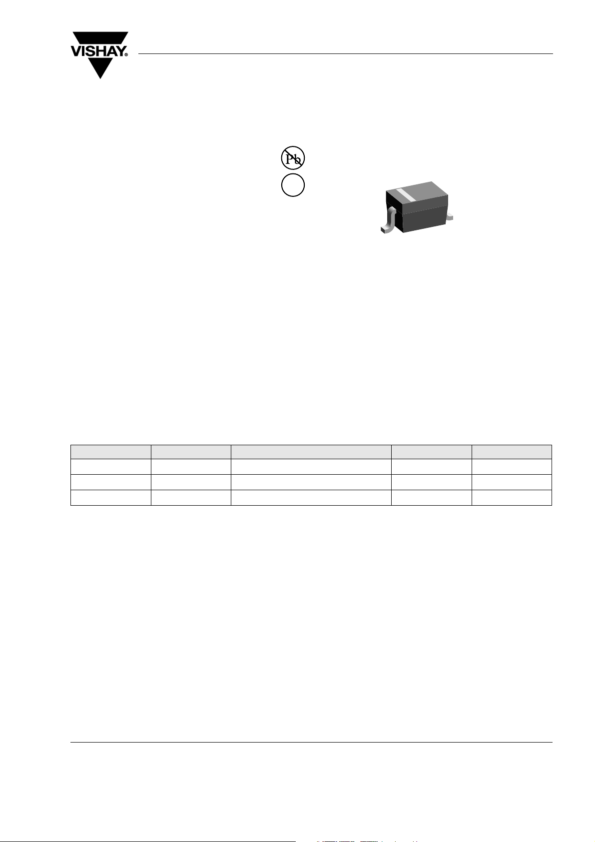
Mechanical Data
Case: SOD323 Plastic case
Weight: approx. 5.0 mg
Packaging Codes/Options:
GS18/10 k per 13" reel (8 mm tape), 10 k/box
GS08/3 k per 7" reel (8 mm tape), 15 k/box
e3
Vishay Semiconductors
20145
Parts Table
Part Type differentiation Ordering code Type Marking Remarks
BAV19WS-V
BAV20WS-V
BAV21WS-V
= 100 V
V
R
V
= 150 V
R
V
= 200 V
R
BAV19WS-V-GS18 or BAV19WS-V-GS08 A8 Tape and Reel
BAV20WS-V-GS18 or BAV20WS-V-GS08 A9 Tape and Reel
BAV21WS-V-GS18 or BAV21WS-V-GS08 AA Tape and Reel
Document Number 85726
Rev. 1.4, 31-Jul-06
www.vishay.com
1
Page 2
BAV19WS-V/20WS-V/21WS-V
Vishay Semiconductors
Absolute Maximum Ratings
T
= 25 °C, unless otherwise specified
amb
Parameter Test condition Par t Symbol Val ue Unit
Continuous reverse voltage
Repetitive peak reverse voltage
= 25 °C I
Forward continuous current
Rectified current (average) half
wave rectification with resist.
T
amb
T
= 25 °C I
amb
load
Repetitive peak forward current f ≥ 50 Hz, θ = 180 °,
T
= 25 °C
amb
Surge forward current
Power dissipation
1) Valid provided that leads are kept at ambient temperature
t < 1 s, T
T
= 25 °C I
j
= 25 °C P
amb
BAV19WS-V
BAV20WS-V
BAV21WS-V
BAV19WS-V
BAV20WS-V
BAV21WS-V
V
V
V
V
RRM
V
RRM
V
RRM
F(AV)
I
FRM
FSM
R
R
R
100 V
150 V
200 V
120 V
200 V
250 V
1)
F
250
200
625
1)
1)
mA
mA
mA
1A
1)
tot
200
mW
Thermal Characteristics
T
= 25 °C, unless otherwise specified
amb
Parameter Test condition Symbol Valu e Unit
Thermal resistance junction to
ambient air
Junction temperature
Storage temperature range
1) Valid provided that leads are kept at ambient temperature
Electrical Characteristics
T
= 25 °C, unless otherwise specified
amb
Parameter Test condition Par t Symbol Min Ty p. Max Unit
Forward voltage I
Leakage current V
Dynamic forward resistance
Diode capacitance
Reverse recovery time I
= 100 mA V
F
= 200 mA V
I
F
= 100 V
R
= 100 V, Tj = 100 °C
V
R
= 150 V
V
R
= 150 V, Tj = 100 °C
V
R
= 200 V
V
R
= 200 V, Tj = 100 °C
V
R
I
= 10 mA r
F
= 0, f = 1 MHz C
V
R
= 30 mA, IR = 30 mA,
F
= 3 mA, RL = 100 Ω
I
rr
R
thJA
T
j
T
stg
BAV19WS-V
BAV19WS-V
BAV20WS-V
BAV20WS-V
BAV21WS-V
BAV21WS-V
F
F
I
R
I
R
I
R
I
R
I
R
I
R
f
D
t
rr
1)
650
1)
150
- 65 to + 150
K/W
°C
1)
°C
1.00 V
1.25 V
100 nA
15 µA
100 nA
15 µA
100 nA
15 µA
5 Ω
1.5 pF
50 ns
www.vishay.com
2
Document Number 85726
Rev. 1.4, 31-Jul-06
Page 3

Typical Characteristics
T
= 25 °C, unless otherwise specified
amb
BAV19WS-V/20WS-V/21WS-V
Vishay Semiconductors
1000
=100°CT
100
F
I - Forward Current (mA)
0.1
0.01
18858
10
1
0 0.4 0.6 0.8 10.2
V
- Forward Voltage (V)
F
j
25°C
Figure 1. Forward Current vs. Forward Voltage
0.3
0.2
ICurrent (rectif.)
O
0.1
0.1
0
OF
I , I - Admissible Forward Current (A)
0 30 60 90 120 150
18859
T
- Ambient Temperature (°C)
amb
IDC current
F
Figure 2. Admissible Forward Current vs. Ambient Temperature
100
(Ω)
10
f
r - Dynamic Forward Resistance
1
1 10010
18861
IF- Forward Current (mA)
Figure 4. Dynamic Forward Resistance vs. Forward Current
1000
100
10
Reverse Voltage
1
RRj
I (T)/I (25 °C) - Leakage Current
0.1
020406080 100 120 140 160 180 200
18862
BAV19WS-VV= 100 V
BAV20WS-VV = 150 V
BAV21WS-VV = 200 V
Tj- Junction Temperature (°C)
R
R
R
Figure 5. Leakage Current vs. Junction Temperature
250
200
150
100
50
tot
0
P - Admissible Power Dissipation (W)
18864
20 40 60 80 100 120 140 160 1800
T
- Ambient Temperature (°C)
amb
200
Figure 3. Admissible Power Dissipation vs. Ambient Temperature
Document Number 85726
Rev. 1.4, 31-Jul-06
2.0
1.8
1.6
1.4
1.2
1.0
0.8
0.6
D
0.4
C - Diode Capacitance (pF)
0.2
0
18863
VR- Reverse Voltage (V)
1100.1
j
Figure 6. Capacitance vs. Reverse Voltage
=25°CT
100
www.vishay.com
3
Page 4

BAV19WS-V/20WS-V/21WS-V
Vishay Semiconductors
Package Dimensions in mm (Inches): SOD323
0.8 (0.031)
1.15 (0.045)
0.10 (0.004)
0.15 (0.006)
0.25 (0.010) min
0.1 (0.004) max
cathode bar
2.85 (0.112)
0.20 (0.008)
2.50 (0.098)
0.40 (0.016)
Document no.: S8-V-3910.02-001 (4)
Rev. 03 - Date: 08.November 2004
17443
1.95 (0.077)
1.60 (0.063)
1.5 (0.059)
foot print recommendation:
0.6 (0.024)
1.1 (0.043)
0.6 (0.024)
1.6 (0.063)
0.6 (0.024)
www.vishay.com
4
Document Number 85726
Rev. 1.4, 31-Jul-06
Page 5

BAV19WS-V/20WS-V/21WS-V
Vishay Semiconductors
Ozone Depleting Substances Policy Statement
It is the policy of Vishay Semiconductor GmbH to
1. Meet all present and future national and international statutory requirements.
2. Regularly and continuously improve the performance of our products, processes, distribution and operating
systems with respect to their impact on the health and safety of our employees and the public, as well as
their impact on the environment.
It is particular concern to control or eliminate releases of those substances into the atmosphere which are
known as ozone depleting substances (ODSs).
The Montreal Protocol (1987) and its London Amendments (1990) intend to severely restrict the use of ODSs
and forbid their use within the next ten years. Various national and international initiatives are pressing for an
earlier ban on these substances.
Vishay Semiconductor GmbH has been able to use its policy of continuous improvements to eliminate the use
of ODSs listed in the following documents.
1. Annex A, B and list of transitional substances of the Montreal Protocol and the London Amendments
respectively
2. Class I and II ozone depleting substances in the Clean Air Act Amendments of 1990 by the Environmental
Protection Agency (EPA) in the USA
3. Council Decision 88/540/EEC and 91/690/EEC Annex A, B and C (transitional substances) respectively.
Vishay Semiconductor GmbH can certify that our semiconductors are not manufactured with ozone depleting
substances and do not contain such substances.
We reserve the right to make changes to improve technical design
and may do so without further notice.
Parameters can vary in different applications. All operating parameters must be validated for each
customer application by the customer. Should the buyer use Vishay Semiconductors products for any
unintended or unauthorized application, the buyer shall indemnify Vishay Semiconductors against all
claims, costs, damages, and expenses, arising out of, directly or indirectly, any claim of personal
damage, injury or death associated with such unintended or unauthorized use.
Vishay Semiconductor GmbH, P.O.B. 3535, D-74025 Heilbronn, Germany
Document Number 85726
Rev. 1.4, 31-Jul-06
www.vishay.com
5
Page 6

Legal Disclaimer Notice
Vishay
Notice
Specifications of the products displayed herein are subject to change without notice. Vishay Intertechnology, Inc.,
or anyone on its behalf, assumes no responsibility or liability for any errors or inaccuracies.
Information contained herein is intended to provide a product description only. No license, express or implied, by
estoppel or otherwise, to any intellectual property rights is granted by this document. Except as provided in Vishay's
terms and conditions of sale for such products, Vishay assumes no liability whatsoever, and disclaims any express
or implied warranty, relating to sale and/or use of Vishay products including liability or warranties relating to fitness
for a particular purpose, merchantability, or infringement of any patent, copyright, or other intellectual property right.
The products shown herein are not designed for use in medical, life-saving, or life-sustaining applications.
Customers using or selling these products for use in such applications do so at their own risk and agree to fully
indemnify Vishay for any damages resulting from such improper use or sale.
Document Number: 91000 www.vishay.com
Revision: 08-Apr-05 1
 Loading...