

BAT54-V/54A-V/54C-V/54S-V
Small Signal Schottky Diodes, Single & Dual
Features
• These diodes feature very low turn-on
voltage and fast switching
• These devices are protected by a PN
junction guard ring against excessive voltage, such as electrostatic discharges
• Lead (Pb)-free component
• Component in accordance to RoHS 2002/95/EC
and WEEE 2002/96/EC
e3
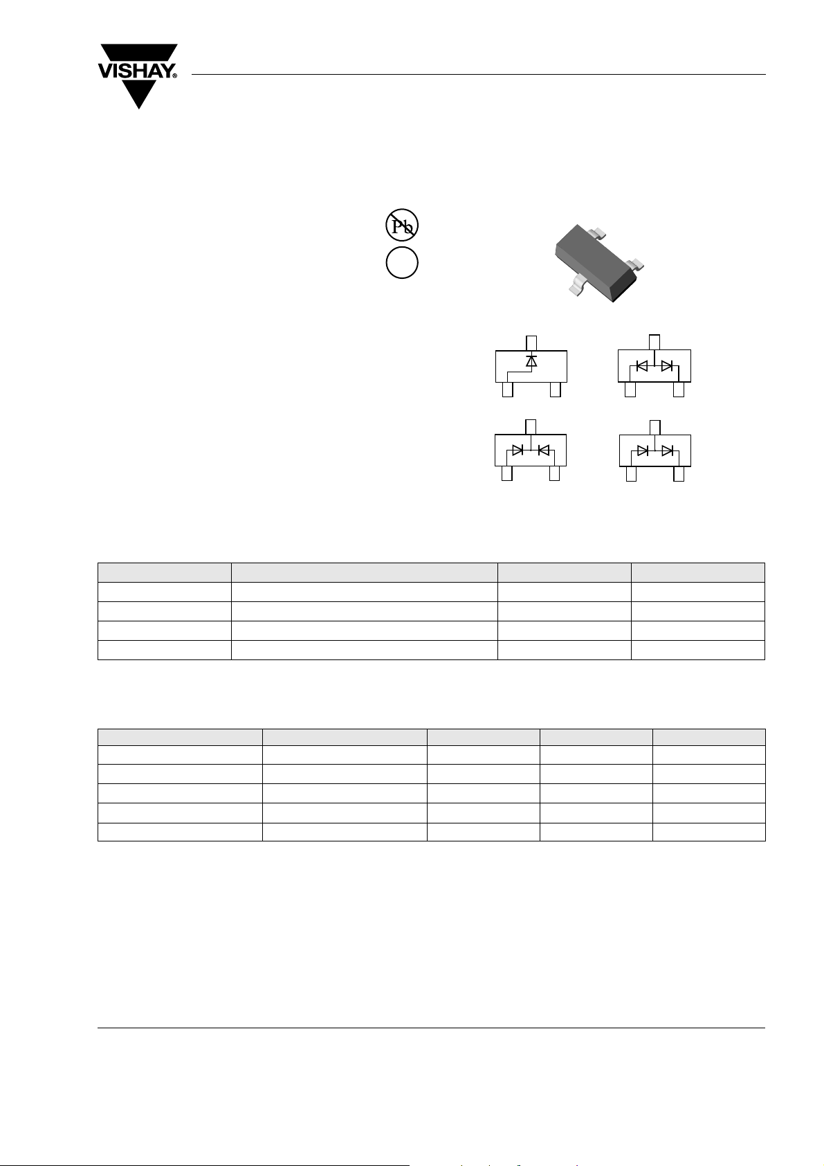
BAT54-V
3
Vishay Semiconductors
BAT54A-V
3
Top View
Mechanical Data
Case: SOT23 Plastic case
Weight: approx. 8.8 mg
Packaging Codes/Options:
GS18/10 k per 13" reel (8 mm tape), 10 k/box
GS08/3 k per 7" reel (8 mm tape), 15 k/box
12
BAT54C-V
3
Top View
12
18034
12
BAT54S-V
3
12
Parts Table
Par t Ordering code Type Marking Remarks
BAT54-V BAT54-V-GS18 or BAT54-V-GS08 L4 Tape and Reel
BAT54A-V BAT54A-V-GS18 or BAT54A-V-GS08 L42 Tape and Reel
BAT54C-V BAT54C-V-GS18 or BAT54C-V-GS08 L43 Tape and Reel
BAT54S-V BAT54S-V-GS18 or BAT54S-V-GS08 L44 Tape and Reel
Absolute Maximum Ratings
T
= 25 °C, unless otherwise specified
amb
Parameter Test condition Symbol Value Unit
Repetitive peak reverse voltage
Forward continuous current
Repetitive peak forward current
t
Surge forward current current
Power dissipation
1)
Device on fiberglass substrate, see layout on next page.
< 1 s I
p
V
RRM
I
FRM
FSM
P
30 V
I
F
tot
1)
200
1)
300
1)
600
230 mW
mA
mA
mA
Document Number 85508
Rev. 1.7, 16-Oct-06
www.vishay.com
1
BAT54-V/54A-V/54C-V/54S-V
Vishay Semiconductors
Thermal Characteristics
T
= 25 °C, unless otherwise specified
amb
Para meter Test condition Symbol Value Unit
Thermal resistance junction to ambiant air
Junction temperature
Storage temperature range
1)
Device on fiberglass substrate, see layout on next page.
Electrical Characteristics
T
= 25 °C, unless otherwise specified
amb
Parameter Test condition Symbol Min Ty p. Max Unit
= 100 µA (pulsed) V
Reverse Breakdown voltage
Leakage current Pulse test t
Forward voltage I
Diode capacitance
Reverse recovery time I
I
R
< 300 µs, δ < 2 % at
p
= 25 V
V
R
= 0.1 mA, tp < 300 µs, δ < 2 % V
F
= 1 mA, tp < 300 µs, δ < 2 % V
I
F
= 10 mA, tp < 300 µs, δ < 2 % V
I
F
= 30 mA, tp < 300 µs, δ < 2 % V
I
F
= 100 mA, tp < 300 µs, δ < 2 % V
I
F
= 1 V, f = 1 MHz C
V
R
= 10 mA to IR = 10 mA,
F
= 1 mA, RL = 100 Ω
i
R
(BR)
I
t
R
thJA
T
j
T
stg
430
1)
K/W
125 °C
- 65 to + 150 °C
30 V
R
F
F
F
F
F
D
rr
2µA
240 mV
320 mV
400 mV
500 mV
800 mV
10 pF
5ns
Layout for R
thJA
test
Thickness:
Fiberglass 1.5 mm (0.059 in.)
Copper leads 0.3 mm (0.012 in.)
15 (0.59)
12 (0.47)
0.8 (0.03)
5 (0.2)
7.5 (0.3)
3 (0.12)
1.5 (0.06)
5.1 (0.2)
1 (0.4)
2 (0.8)
1 (0.4)
2 (0.8)
17451
www.vishay.com
2
Document Number 85508
Rev. 1.7, 16-Oct-06

Typical Characteristics
T
= 25 °C, unless otherwise specified
amb
1000
= 125 °CT
j
100
BAT54-V/54A-V/54C-V/54S-V
Vishay Semiconductors
10
1
F
0.1
I - Forward Voltage (mA)
0.01
0 0.4
18867
- 40 °C
25 °C
0.6 1.2 1.4
V
- Forward Current (V)
F
0.8 10.2
Figure 1. Typical Forward Voltage Forward Current at Various
Temperatures
14
12
10
8
6
4
D
2
C - Typical Capacitance (pF)
0
04 8 12 16 20 24 28
18868
Figure 2. Diode Capacitance vs. Reverse Voltage V
VR-Reverse Voltage (V)
R
I-Reverse Current (µA)
18869
1000
100
R
0.01
10
1
0.1
=125°CT
j
100°C
75°C
50°C
25°C
510152002530
V
-Reverse Voltage (V)
R
Figure 3. Typical Variation of Reverse Current at Various
Temperatures
Document Number 85508
Rev. 1.7, 16-Oct-06
www.vishay.com
3

BAT54-V/54A-V/54C-V/54S-V
Vishay Semiconductors
Package Dimensions in mm (Inches): SOT23
17418
www.vishay.com
4
Document Number 85508
Rev. 1.7, 16-Oct-06

BAT54-V/54A-V/54C-V/54S-V
Vishay Semiconductors
Ozone Depleting Substances Policy Statement
It is the policy of Vishay Semiconductor GmbH to
1. Meet all present and future national and international statutory requirements.
2. Regularly and continuously improve the performance of our products, processes, distribution and operating
systems with respect to their impact on the health and safety of our employees and the public, as well as
their impact on the environment.
It is particular concern to control or eliminate releases of those substances into the atmosphere which are
known as ozone depleting substances (ODSs).
The Montreal Protocol (1987) and its London Amendments (1990) intend to severely restrict the use of ODSs
and forbid their use within the next ten years. Various national and international initiatives are pressing for an
earlier ban on these substances.
Vishay Semiconductor GmbH has been able to use its policy of continuous improvements to eliminate the use
of ODSs listed in the following documents.
1. Annex A, B and list of transitional substances of the Montreal Protocol and the London Amendments
respectively
2. Class I and II ozone depleting substances in the Clean Air Act Amendments of 1990 by the Environmental
Protection Agency (EPA) in the USA
3. Council Decision 88/540/EEC and 91/690/EEC Annex A, B and C (transitional substances) respectively.
Vishay Semiconductor GmbH can certify that our semiconductors are not manufactured with ozone depleting
substances and do not contain such substances.
We reserve the right to make changes to improve technical design
and may do so without further notice.
Parameters can vary in different applications. All operating parameters must be validated for each
customer application by the customer. Should the buyer use Vishay Semiconductors products for any
unintended or unauthorized application, the buyer shall indemnify Vishay Semiconductors against all
claims, costs, damages, and expenses, arising out of, directly or indirectly, any claim of personal
damage, injury or death associated with such unintended or unauthorized use.
Vishay Semiconductor GmbH, P.O.B. 3535, D-74025 Heilbronn, Germany
Document Number 85508
Rev. 1.7, 16-Oct-06
www.vishay.com
5

Legal Disclaimer Notice
Vishay
Notice
Specifications of the products displayed herein are subject to change without notice. Vishay Intertechnology, Inc.,
or anyone on its behalf, assumes no responsibility or liability for any errors or inaccuracies.
Information contained herein is intended to provide a product description only. No license, express or implied, by
estoppel or otherwise, to any intellectual property rights is granted by this document. Except as provided in Vishay's
terms and conditions of sale for such products, Vishay assumes no liability whatsoever, and disclaims any express
or implied warranty, relating to sale and/or use of Vishay products including liability or warranties relating to fitness
for a particular purpose, merchantability, or infringement of any patent, copyright, or other intellectual property right.
The products shown herein are not designed for use in medical, life-saving, or life-sustaining applications.
Customers using or selling these products for use in such applications do so at their own risk and agree to fully
indemnify Vishay for any damages resulting from such improper use or sale.
Document Number: 91000 www.vishay.com
Revision: 08-Apr-05 1
 Loading...