

Page 1
www.vishay.com
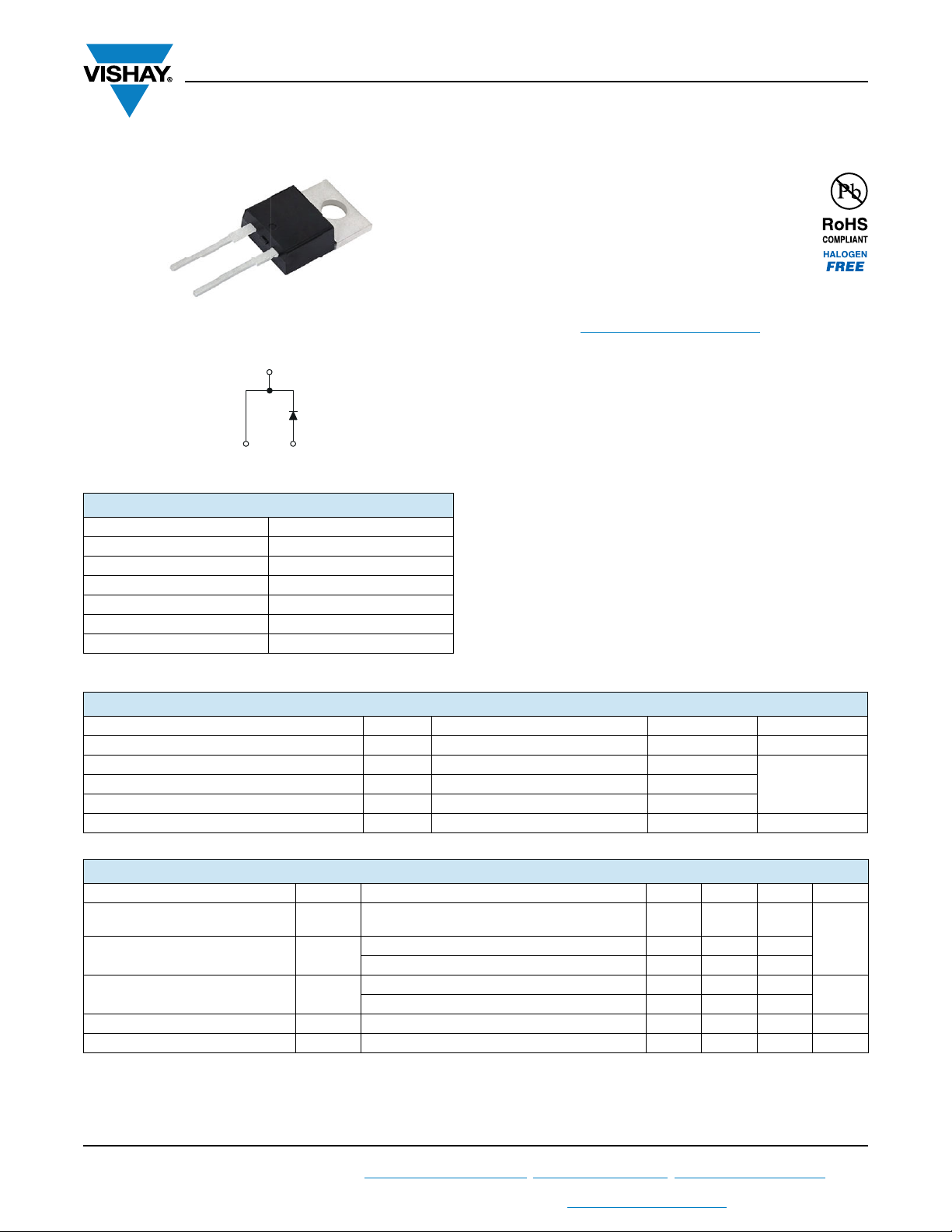
2L TO-220AC
1
2
3
Anode
1
3
Cathode
Base
cathode
2
VS-8ETH06-M3
Vishay Semiconductors
Hyperfast Rectifier, 8 A FRED Pt
PRIMARY CHARACTERISTICS
I
F(AV)
V
R
V
at I
F
F
t
typ. 18 ns
rr
T
max. 175 °C
J
Package 2L TO-220AC
Circuit configuration Single
8 A
600 V
1.3 V
®
FEATURES
• Hyperfast recovery time
• Low forward voltage drop
• 175 °C operating junction temperature
• Low leakage current
• Designed and qualified according to JEDEC
• Material categorization: for definitions of compliance
please see www.vishay.com/doc?99912
DESCRIPTION / APPLICATIONS
State of the art hyperfast recovery rectifiers designed with
optimized performance of forward voltage drop, hyperfast
recovery time, and soft recovery.
The planar structure and the platinum doped life time control
guarantee the best overall performance, ruggedness and
reliability characteristics.
These devices are intended for use in PFC boost stage in the
AC/DC section of SMPS, inverters or as freewheeling
diodes.
Their extremely optimized stored charge and low recovery
current minimize the switching losses and reduce over
dissipation in the switching element and snubbers.
®
-JESD 47
ABSOLUTE MAXIMUM RATINGS
PARAMETER SYMBOL TEST CONDITIONS VALUES UNITS
Repetitive peak reverse voltage V
Average rectified forward current I
Repetitive peak forward current I
Operating junction and storage temperatures T
F(AV)
FSM
, T
J
RRM
TC = 144 °C 8
TJ = 25 °C 90
FM
Stg
600 V
16
-65 to +175 °C
ELECTRICAL SPECIFICATIONS (TJ = 25 °C unless otherwise specified)
PARAMETER SYMBOL TEST CONDITIONS MIN. TYP. MAX. UNITS
Breakdown voltage,
blocking voltage
Forward voltage V
Reverse leakage current I
Junction capacitance C
Series inductance L
Revision: 23-Nov-17
For technical questions within your region: DiodesAmericas@vishay.com
THIS DOCUMENT IS SUBJECT TO CHANGE WITHOUT NOTICE. THE PRODUCTS DESCRIBED HEREIN AND THIS DOCUMENT
ARE SUBJECT TO SPECIFIC DISCLAIMERS, SET FORTH AT www.vishay.com/doc?91000
V
,
BR
V
IR = 100 μA 600 - -
R
IF = 8 A - 2.0 2.4
F
I
= 8 A, TJ = 150 °C - 1.3 1.8
F
VR = VR rated - 0.3 50
R
T
S
= 150 °C, VR = VR rated - 55 500
T
J
VR = 600 V - 17 - pF
Measured lead to lead 5 mm from package body - 8.0 - nH
1
, DiodesAsia@vishay.com, DiodesEurope@vishay.com
Document Number: 96177
ANon-repetitive peak surge current I
V
μA
Page 2
VS-8ETH06-M3
1
10
TJ = 175 °C
T
J
= 150 °C
T
J
= 25 °C
01
VF - Forward Voltage Drop (V)
I
F
- Instantaneous Forward Current (A)
100
23
4
0.1
www.vishay.com
DYNAMIC RECOVERY CHARACTERISTICS (TC = 25 °C unless otherwise specified)
PARAMETER SYMBOL TEST CONDITIONS MIN. TYP. MAX. UNITS
IF = 1 A, dIF/dt = 100 A/μs, VR = 30 V - 18 22
I
= 8 A, dIF/dt = 100 A/μs, VR = 30 V - 20 25
Reverse recovery time t
Peak recovery current I
Reverse recovery charge Q
Reverse recovery time t
Peak recovery current I
Reverse recovery charge Q
rr
RRM
rr
rr
RRM
rr
F
T
= 25 °C
J
= 125 °C - 40 -
T
J
TJ = 25 °C - 2.4 -
= 125 °C - 4.8 -
T
J
TJ = 25 °C - 25 -
= 125 °C - 120 -
T
J
TJ = 125 °C
I
= 8 A
F
dI
/dt = 200 A/μs
F
V
= 390 V
R
= 8 A
I
F
dI
/dt = 600 A/μs
F
V
= 390 V
R
THERMAL - MECHANICAL SPECIFICATIONS
PARAMETER SYMBOL TEST CONDITIONS MIN. TYP. MAX. UNITS
Maximum junction and storage
temperature range
Thermal resistance, junction-to-case R
Thermal resistance, junction-to-ambient
per leg
Thermal resistance, case-to-heatsink R
Weight
Mounting torque
Marking device Case style 2L TO-220AC 8ETH06
T
, T
J
Stg
-1.42°C/W
thJC
R
thJA
thCS
Typical socket mount - - 70
Mounting surface, flat, smooth, and
greased
Vishay Semiconductors
-25-
-33-ns
-12- A
- 220 - nC
-65 - 175 °C
-0.5-
-2.0- g
-0.07- oz.
6.0
(5.0)
-
12
(10)
ns
A
nC
kgf · cm
(lbf · in)
1000
100
10
1
0.1
- Reverse Current (µA)
R
0.01
I
0.001
0 200 400
100
TJ = 175 °C
TJ = 150 °C
TJ = 125 °C
TJ = 100 °C
TJ = 25 °C
300
VR - Reverse Voltage (V)
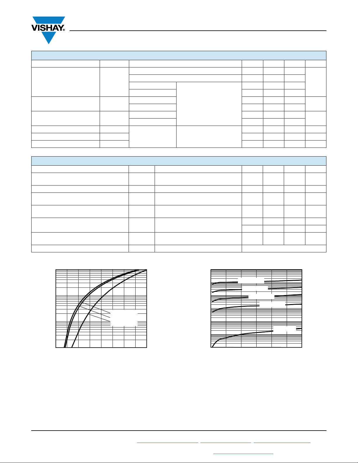
Fig. 1 - Typical Forward Voltage Drop Characteristics Fig. 2 - Typical Values of Reverse Current vs. Reverse Voltage
Revision: 23-Nov-17
For technical questions within your region: DiodesAmericas@vishay.com
THIS DOCUMENT IS SUBJECT TO CHANGE WITHOUT NOTICE. THE PRODUCTS DESCRIBED HEREIN AND THIS DOCUMENT
ARE SUBJECT TO SPECIFIC DISCLAIMERS, SET FORTH AT www.vishay.com/doc?91000
2
, DiodesAsia@vishay.com, DiodesEurope@vishay.com
Document Number: 96177
600500
Page 3
www.vishay.com
100
1000
0 200 400 500 600
10
VR - Reverse Voltage (V)
C
T
- Junction Capacitance (pF)
300100
TJ = 25 °C
10
VS-8ETH06-M3
Vishay Semiconductors
Fig. 3 - Typical Junction Capacitance vs. Reverse Voltage
1
0.1
- Thermal Impedance (°C/W)
thJC
Z
0.01
0.00001 0.0001 0.001 0.01 0.1 1
Single pulse
(thermal resistance)
Fig. 4 - Maximum Thermal Impedance Z
180
170
160
150
140
130
Allowable Case Temperature (°C)
See note (1)
120
02 6 1012
I
F(AV)
Square wave (D = 0.50)
applied
Rated V
R
48
- Average Forward Current (A)
DC
Fig. 5 - Maximum Allowable Case Temperature vs.
Average Forward Current
D = 0.50
D = 0.20
D = 0.10
D = 0.05
D = 0.02
D = 0.01
t1 - Rectangular Pulse Duration (s)
Characteristics
thJC
20
18
16
14
12
10
8
6
4
Average Power Loss (W)
2
0
02 6 1012
Fig. 6 - Forward Power Loss Characteristics
P
DM
t
1
t
2
Notes:
1. Duty factor D = t
2. Peak TJ = PDM x Z
DC
48
I
- Average Forward Current (A)
F(AV)
1/t2
thJC
.
+ T
C
RMS limit
.
D = 0.01
D = 0.02
D = 0.05
D = 0.10
D = 0.20
D = 0.50
Note
(1)
Formula used: TC = TJ - (Pd + Pd
Pd = forward power loss = I
Pd
= inverse power loss = VR1 x IR (1 - D); IR at VR1 = rated V
REV
Revision: 23-Nov-17
For technical questions within your region: DiodesAmericas@vishay.com
THIS DOCUMENT IS SUBJECT TO CHANGE WITHOUT NOTICE. THE PRODUCTS DESCRIBED HEREIN AND THIS DOCUMENT
) x R
x VFM at (I
F(AV)
REV
;
thJC
/D) (see fig. 5);
F(AV)
R
3
Document Number: 96177
, DiodesAsia@vishay.com, DiodesEurope@vishay.com
ARE SUBJECT TO SPECIFIC DISCLAIMERS, SET FORTH AT www.vishay.com/doc?91000
Page 4

www.vishay.com
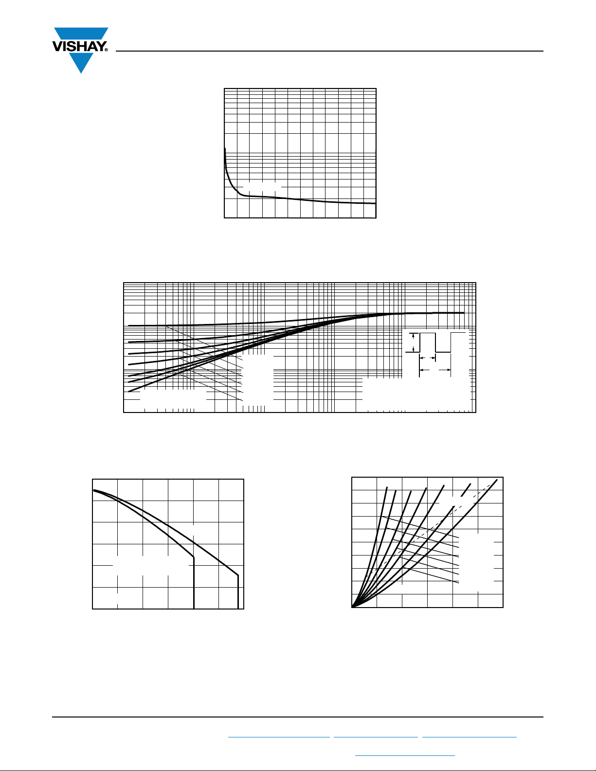
100 1000
Q
rr
(nC)
dIF/dt (A/µs)
400
0
IF = 16 A
I
F
= 8 A
300
200
100
50
VR = 390 V
T
J
= 125 °C
T
J
= 25 °C
350
250
150
Q
rr
0.5 I
RRM
di
(rec)M
/dt
0.75 I
RRM
I
RRM
t
rr
t
b
t
a
I
F
diF/dt
0
(1)
(2)
(3)
(4)
(5)
(1) di
F
/dt - rate of change of current
through zero crossing
(2) I
RRM
- peak reverse recovery current
(3) t
rr
- reverse recovery time measured
from zero crossing point of negative
going I
F
to point where a line passing
through 0.75 I
RRM
and 0.50 I
RRM
extrapolated to zero current.
(4) Q
rr
- area under curve dened by t
rr
and I
RRM
trr x I
RRM
2
Qrr =
(5) di
(rec)M
/dt - peak rate of change of
current during t
b
portion of t
rr
VS-8ETH06-M3
Vishay Semiconductors
60
VR = 390 V
= 125 °C
T
J
= 25 °C
50
T
J
40
(ns)
rr
t
30
20
IF = 16 A
= 8 A
I
F
10
100 1000
dIF/dt (A/µs)
Fig. 7 - Typical Reverse Recovery Time vs. dIF/dt Fig. 8 - Typical Stored Charge vs. dIF/dt
Revision: 23-Nov-17
For technical questions within your region: DiodesAmericas@vishay.com
THIS DOCUMENT IS SUBJECT TO CHANGE WITHOUT NOTICE. THE PRODUCTS DESCRIBED HEREIN AND THIS DOCUMENT
Fig. 9 - Reverse Recovery Waveform and Definitions
ARE SUBJECT TO SPECIFIC DISCLAIMERS, SET FORTH AT www.vishay.com/doc?91000
4
, DiodesAsia@vishay.com, DiodesEurope@vishay.com
Document Number: 96177
Page 5

www.vishay.com
ORDERING INFORMATION TABLE
VS-8ETH06-M3
Vishay Semiconductors
Device code
VS-8 E T H06-M3
51 32 4 6 7
1 -Vishay Semiconductors product
2 - Current rating (8 = 8 A)
3 - E = single
4
- T = TO-220, D2PAK (TO-263AB)
5 - H = hyperfast recovery
6 - Voltage rating (06 = 600 V)
7
- Environmental digit:
-M3 = halogen-free, RoHS-compliant, and termination lead (Pb)-free
ORDERING INFORMATION (Example)
PREFERRED P/N QUANTITY PER T/R MINIMUM ORDER QUANTITY PACKAGING DESCRIPTION
VS-8ETH06-M3 50 1000 Antistatic plastic tube
LINKS TO RELATED DOCUMENTS
Dimensions www.vishay.com/doc?96156
Part marking information www.vishay.com/doc?95391
Revision: 23-Nov-17
For technical questions within your region: DiodesAmericas@vishay.com
THIS DOCUMENT IS SUBJECT TO CHANGE WITHOUT NOTICE. THE PRODUCTS DESCRIBED HEREIN AND THIS DOCUMENT
ARE SUBJECT TO SPECIFIC DISCLAIMERS, SET FORTH AT www.vishay.com/doc?91000
5
, DiodesAsia@vishay.com, DiodesEurope@vishay.com
Document Number: 96177
Page 6

www.vishay.com
12
C
C
D
D
2 x b22 x b
(b, b2)
b1, b3
0.014 AB
M M
0.015 AB
M M
Conforms to JEDEC® outline TO-220AC
(6)
(6)
(6)
(7)
L1
(2)
Detail B
Section C - C and D - D
Base metal Plating
(4)
(4)
c1
c
(6)
(6)
Ø P
E
Q
D
L
c
D1
e
e1
2 x
A
B
A
A
A
C
A2
A1
Thermal pad
H1
(E)
(H1)
D2
Detail B
E1
View A - A
Lead tip
DIMENSIONS in millimeters and inches
Outline Dimensions
Vishay Semiconductors
2L TO-220AC
SYMBOL
Notes
(1)
(2)
(3)
(4)
(5)
(6)
(7)
Revision: 06-Dec-17
MILLIMETERS INCHES
MIN. MAX. MIN. MAX. MIN. MAX. MIN. MAX.
NOTES SYMBOL
MILLIMETERS INCHES
NOTES
A 4.25 4.65 0.167 0.183 D2 11.68 12.88 0.460 0.507 6
A1 1.14 1.40 0.045 0.055 E 10.11 10.51 0.398 0.414 3, 6
A2 2.50 2.92 0.098 0.115 E1 6.86 8.89 0.270 0.350 6
b 0.69 1.01 0.027 0.040 e 2.41 2.67 0.095 0.105
b1 0.38 0.97 0.015 0.038 4 e1 4.88 5.28 0.192 0.208
b2 1.20 1.73 0.047 0.068 H1 6.09 6.48 0.240 0.255 6, 7
b3 1.14 1.73 0.045 0.068 4 L 13.52 14.02 0.532 0.552
c 0.36 0.61 0.014 0.024 L1 3.32 3.82 0.131 0.150 2
c1 0.36 0.56 0.014 0.022 4 Ø P 3.54 3.91 0.139 0.154
D 14.85 15.35 0.585 0.604 3 Q 2.60 3.00 0.102 0.118
D1 8.38 9.02 0.330 0.355
Dimensioning and tolerancing as per ASME Y14.5M-1994
Lead dimension and finish uncontrolled in L1
Dimension D, D1, and E do not include mold flash. Mold flash shall not exceed 0.127 mm (0.005") per side. These dimensions are measured
at the outermost extremes of the plastic body
Dimension b1, b3, and c1 apply to base metal only
Controlling dimensions: inches
Thermal pad contour optional within dimensions E, H1, D2, and E1
Outline conforms to JEDEC® TO-220, except D2 (minimum)
THIS DOCUMENT IS SUBJECT TO CHANGE WITHOUT NOTICE. THE PRODUCTS DESCRIBED HEREIN AND THIS DOCUMENT
1
For technical questions within your region: DiodesAmericas@vishay.com
ARE SUBJECT TO SPECIFIC DISCLAIMERS, SET FORTH AT www.vishay.com/doc?91000
Document Number: 96156
, DiodesAsia@vishay.com, DiodesEurope@vishay.com
Page 7

Legal Disclaimer Notice
www.vishay.com
Vishay
Disclaimer
ALL PRODUCT, PRODUCT SPECIFICATIONS AND DATA ARE SUBJECT TO CHANGE WITHOUT NOTICE TO IMPROVE
RELIABILITY, FUNCTION OR DESIGN OR OTHERWISE.
Vishay Intertechnology, Inc., its affiliates, agents, and employees, and all persons acting on its or their behalf (collectively,
“Vishay”), disclaim any and all liability for any errors, inaccuracies or incompleteness contained in any datasheet or in any other
disclosure relating to any product.
Vishay makes no warranty, representation or guarantee regarding the suitability of the products for any particular purpose or
the continuing production of any product. To the maximum extent permitted by applicable law, Vishay disclaims (i) any and all
liability arising out of the application or use of any product, (ii) any and all liability, including without limitation special,
consequential or incidental damages, and (iii) any and all implied warranties, including warranties of fitness for particular
purpose, non-infringement and merchantability.
Statements regarding the suitability of products for certain types of applications are based on Vishay’s knowledge of
typical requirements that are often placed on Vishay products in generic applications. Such statements are not binding
statements about the suitability of products for a particular application. It is the customer’s responsibility to validate that a
particular product with the properties described in the product specification is suitable for use in a particular application.
Parameters provided in datasheets and / or specifications may vary in different applications and performance may vary over
time. All operating parameters, including typical parameters, must be validated for each customer application by the customer’s
technical experts. Product specifications do not expand or otherwise modify Vishay’s terms and conditions of purchase,
including but not limited to the warranty expressed therein.
Except as expressly indicated in writing, Vishay products are not designed for use in medical, life-saving, or life-sustaining
applications or for any other application in which the failure of the Vishay product could result in personal injury or death.
Customers using or selling Vishay products not expressly indicated for use in such applications do so at their own risk.
Please contact authorized Vishay personnel to obtain written terms and conditions regarding products designed for
such applications.
No license, express or implied, by estoppel or otherwise, to any intellectual property rights is granted by this document
or by any conduct of Vishay. Product names and markings noted herein may be trademarks of their respective owners.
© 2017 VISHAY INTERTECHNOLOGY, INC. ALL RIGHTS RESERVED
Revision: 08-Feb-17
1
Document Number: 91000
 Loading...