

Page 1
Ultrafast Rectifier
Base
Common
Cathode
Anode Anode
Common
Cathode
13
2
1
2
2
Document Number: 93023
www.vishay.com
1
Bulletin PD-20637 rev. A 12/06
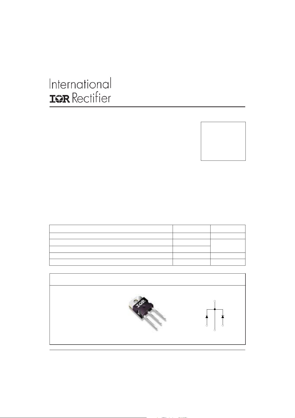
70CRU04
Features
• Two Common-Cathode Diodes
• Ultrafast Reverse Recovery
• Ultrasoft Reverse Recovery Current Shape
• Low Forward Voltage Drop
• Low Leakage Current
• Optimized for Power Conversion: Welding and Industrial SMPS Applications
• Up to 175°C Operating Junction Temperature
Description/ Applications
The 70CRU04 integrates two state-of-the-art International Rectifier’s Ultrafast recovery rectifiers in the commoncathode configuration. The planar structure of the diodes, and the platinum doping life-time control, provide a
Ultrasoft recovery current shape, together with the best overall performance, ruggedness and reliability characteristics.
These devices are thus intended for high frequency applications in which the switching energy is designed not to
be predominant portion of the total energy, such as in the output rectification stage of Welding machines, SMPS,
DC-DC converters. Their extremely optimized stored charge and low recovery current reduce both overdissipation in the switching elements (and snubbers) and EMI/RFI.
t
= 38ns
rr
I
= 70Amp
F(AV)
@TC = 116°C
VR = 400V
Absolute Maximum Ratings
Parameters Max Units
V
R
I
F(AV)
I
FSM
P
D
TJ, T
Cathode to Anode Voltage 400 V
Continuous Forward Current TC = 116°C Per Diode 35 A
Single Pulse Forward Current TC = 25°C Per Diode 300
Maximum Power Dissipation TC = 100°C Per Module 47 W
Operating Junction and Storage Temperatures - 55 to 175 °C
STG
Case Styles
TO-218
Page 2
70CRU04
Document Number: 93023
www.vishay.com
2
Bulletin PD-20637 rev. A 12/06
Electrical Characteristics per Diode @ T
= 25°C (unless otherwise specified)
J
Parameters Min Typ Ma x Units Test Conditions
VBR, VrBreakdown Voltage, 400 - - V IR = 100μA
Blocking Voltage
V
F
Forward Voltage - 1.11 1.32 V IF = 35A
- 0.98 1.14 V IF = 35A, TJ = 125°C
- 0.92 1.05 V IF = 35A, TJ = 175°C
I
R
Reverse Leakage Current - - 100 μAVR = VR Rated
--2mATJ = 150°C, VR = VR Rated
C
T
Dynamic Recovery Characteristics per Diode @ T
Junction Capacitance - 70 - pF VR = 400V
= 25°C (unless otherwise specified)
J
Parameters Min Typ Ma x Units Test Conditions
t
t
I
RRM
Q
rr
rr
rr
Reverse Recovery Time - 32 38 ns TJ = 25°C
Reverse Recovery Time - 72 - ns TJ = 25°C
- 130 - TJ = 125°C
Peak Recovery Current - 7.7 - A TJ = 25°C
- 16.5 - TJ = 125°C
Reverse Recovery Charge - 0.28 - μCTJ = 25°C
- 1.08 - TJ = 125°C
I
= 1A
F
VR = 30V
diF /dt = 200A/μs
I
= 35A
F
VR = 200V
diF /dt = 200A/μs
Thermal - Mechanical Characteristics
Parameters Min Typ Max Units
R
thJC
R
thJC
R
thCS
Wt Weight - 4 - g
T Mounting Torque 1.2 - 2.4 N * m
(1) Mounting Surface, Flat, Smooth and Greased
Thermal Resistance, Junction to Case Per Diode - 0.8 1.6 K/W
Thermal Resistance, Junction to Case Both Diodes - 0.4 0.8
(1)
Thermal Resistance, Case to Heatsink - 0.2 -
- 0.13 - (oz)
10 - 20 lbf.in
Marking Device 70CRU04
Page 3
70CRU04
1
1 10 100 1000
1
0 0.5 1 1.5 2 2.5 3
0
0
0
50 100 150 200 250 300 350 400
Document Number: 93023
www.vishay.com
3
Bulletin PD-20637 rev. A 12/06
000
(A)
F
100
10
Instantaneous Forward Current - I
Tj = 175˚C
Tj = 125˚C
Tj = 25˚C
1000
Tj = 175˚C
100
( μA)
R
10
150˚C
125˚C
1
0.1
Reverse Current - I
0.01
25˚C
.001
Reverse Voltage - VR (V)
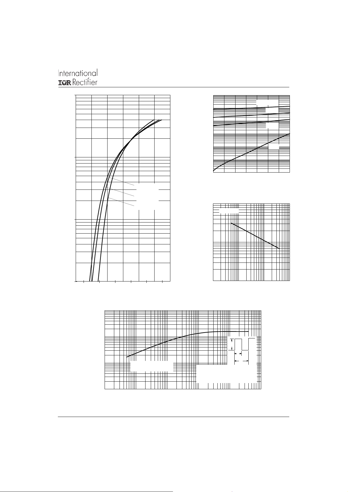
Fig. 2 - Typical Values Of Reverse Current
Vs. Reverse Voltage
000
Tj = 25˚C
(pF)
T
100
Junction Capacitance - C
1
Forward Voltage Drop - VFM (V)
Fig. 1 - Typical Forward Voltage Drop Characteristics
(Per Diode)
10
Reverse Voltage - VR (V)
Fig. 3 - Typical Junction Capacitance
Vs. Reverse Voltage
10
(°C/W)
thJC
1
0.1
Thermal Impedance Z
.01
0.0001 0.001 0.01 0.1 1 1
Single Pulse
(Thermal Resistance)
Notes:
1. Duty factor D = t1/ t2
2. Peak Tj = Pdm x ZthJC + Tc
P
DM
t
1
t
2
t1, Rectangular Pulse Duration (Seconds)
Fig. 4 - Max. Thermal Impedance Z
Characteristics (Per Diode)
thJC
Page 4

70CRU04
1
1
1
1
1
1
1
1
1
0 5 10 15 20 25 30 35 40
1
1
2
2
3
3
4
0 5 10 15 20 25 30 35
1
1
1
1
1
1
100 1000
1
1
2
2
100 1000
Document Number: 93023
www.vishay.com
4
Bulletin PD-20637 rev. A 12/06
80
70
60
50
40
DC
30
Square wave (D = 0.50)
20
Rated Vr applied
10
Allowable Case Temperature (°C)
see note (3)
00
Average Forward Current - I
Fig. 5 - Max. Allowable Case Temperature
Vs. Average Forward Current
50
40
If = 35A
Vrr = 200V
30
20
Tj = 125˚C
10
F(AV)
(A)
0
5
RMS Limit
0
5
0
5
0
Average Power Loss ( Watts )
5
D = 0.01
D = 0.02
D = 0.05
D = 0.10
D = 0.20
D = 0.50
DC
0
Average Forward Current - I
F(AV)
(A)
Fig. 6 - Forward Power Loss Characteristics
500
If = 35A
Vrr = 200V
000
500
Tj = 125˚C
00
trr ( ns )
90
80
70
60
50
Fig. 7 - Typical Reverse Recovery vs. di
(3) Formula used: T
Pd = Forward Power Loss = I
Pd
REV
Tj = 25˚C
di
/dt (A/μs )
F
= TJ - (Pd + Pd
C
= Inverse Power Loss = VR1 x IR (1 - D); IR @ V
F(AV)
) x R
REV
x VFM @ (I
thJC
;
F(AV)
/ D) (see Fig. 6);
/dt
F
= rated V
R1
Qrr ( nC )
000
Tj = 25˚C
500
0
di F /dt (A/μs )
Fig. 8 - Typical Stored Charge vs. di
R
/dt
F
Page 5

Outline Table
Document Number: 93023
www.vishay.com
5
70CRU04
Bulletin PD-20637 rev. A 12/06
Marking Information
EXAMPLE:
THIS IS A 70CRU04
LOT CODE 0J54
ASSEMBLED ON WW 19, 2001
IN THE ASSEMBLY LINE "C"
Dimensions in inches (and milimetres)
70CRU04
0119C
0J54
ASSEMBLY
LOT CODE
PART NUMBER
INTERNATIONAL
RECTIFIER
LOGO
DATE CODE
YEAR 01 = 2001
WEEK 19
LINE C
Page 6

70CRU04
Document Number: 93023
www.vishay.com
6
Bulletin PD-20637 rev. A 12/06
Ordering Information Table
Device Code
70 C R U 04 -
2
1
1 - Current Rating (70 = 70A)
2 - Common Cathode
3 - TO-218
4 - Ultrafast Recovery
5 - Voltage Rating (04 = 400V)
6 - y none = Standard Production
3
5
4
y PbF = Lead-Free
Tube Standard Pack Quantity : 30 pieces
6
This product has been designed and qualified for Industrial Level.
Data and specifications subject to change without notice.
Qualification Standards can be found on IR's Web site.
IR WORLD HEADQUARTERS: 233 Kansas St., El Segundo, California 90245, USA Tel: (310) 252-7105
TAC Fax: (310) 252-7309
12/06
Page 7

Legal Disclaimer Notice
Vishay
Notice
The products described herein were acquired by Vishay Intertechnology, Inc., as part of its acquisition of
International Rectifier’s Power Control Systems (PCS) business, which closed in April 2007. Specifications of the
products displayed herein are pending review by Vishay and are subject to the terms and conditions shown below.
Specifications of the products displayed herein are subject to change without notice. Vishay Intertechnology, Inc., or
anyone on its behalf, assumes no responsibility or liability for any errors or inaccuracies.
Information contained herein is intended to provide a product description only. No license, express or implied, by
estoppel or otherwise, to any intellectual property rights is granted by this document. Except as provided in Vishay's
terms and conditions of sale for such products, Vishay assumes no liability whatsoever, and disclaims any express
or implied warranty, relating to sale and/or use of Vishay products including liability or warranties relating to fitness
for a particular purpose, merchantability, or infringement of any patent, copyright, or other intellectual property right.
The products shown herein are not designed for use in medical, life-saving, or life-sustaining applications.
Customers using or selling these products for use in such applications do so at their own risk and agree to fully
indemnify Vishay for any damages resulting from such improper use or sale.
International Rectifier
are registered trademarks of International Rectifier Corporation in the U.S. and other countries. All other product
names noted herein may be trademarks of their respective owners.
®
, IR®, the IR logo, HEXFET®, HEXSense®, HEXDIP®, DOL®, INTERO®, and POWIRTRAIN
®
Document Number: 99901 www.vishay.com
Revision: 12-Mar-07 1
 Loading...