

Page 1

6N137 / VO2601 / 11 / VO2630 / 31 / VO4661
High Speed Optocoupler, 10 Mbd
Features
• Choice of CMR performance of 10 kV/µs,
5 kV/µs, and 100 V/µs
• High speed: 10 Mbd typical
•+ 5 V CMOS compatibility
• Guaranteed AC and DC performance over temperature: - 40 to + 100 °C Temp. Range
• Pure tin leads
• Meets IEC60068-2-42 (SO
IEC60068-2-43 (H
S) requirements
2
) and
2
• Low input current capability: 5 mA
• Lead (Pb)-free component
• Component in accordance to RoHS 2002/95/EC
and WEEE 2002/96/EC
Agency Approvals
• UL1577, File No. E52744 System Code H or J,
Double Protection
• CUL - File No. E52744, equivalent to CSA bulletin
5A
• DIN EN 60747-5-2 (VDE0884)
• Reinforced insulation rating per IEC60950
2.10.5.1
• VDE available with Option 1
Applications
Microprocessor System Interface
PLC, ATE input/output isolation
Computer peripheral interface
Digital Fieldbus Isolation: CC-Link, DeviceNet,
Profibus, SDS
High speed A/D and D/A conversion
AC Plasma Display Panel Level Shifting
Multiplexed Data Transmission
Digital control power supply
Ground loop elimination
Description
The 6N137, VO2601 and VO2611 are single channel
10 Mbd optocouplers utilizing a high efficient input
LED coupled with an integrated optical photodiode IC
detector. The detector has an open drain NMOS-transistor output, providing less leakage compared to an
e3
Vishay Semiconductors
Single channel
1
NC
2
A
3
C
4
NC
6N137, VO2601, VO2611
8
7
6
5
V
CC
V
E
V
O
GND
18921_5
open collector Schottky clamped transistor output.
The VO2630, VO2631 and VO4661 are dual channel
10MBd optocouplers. For the single channel type, an
enable function on pin 7 allows the detector to be
strobed. The internal shield provides a guaranteed
common mode transient immunity of 5 kV/µs for the
VO2601 and VO2631 and 10 kV/µs for the VO2611
and VO4661. The use of a 0.1 µF bypass capacitor
connected between pin 5 and 8 is recommended.
Dual channel
1
A1
2
C1
3
C2
4
A2
VO2630, VO2631, VO4661
8
7
6
5
V
CC
V
O1
V
O2
GND
Order Information
Part Remarks
6N137 100 V/µs, Single channel, DIP-8
6N137-X006 100 V/µs, Single channel, DIP-8 400 mil
6N137-X007 100 V/µs, Single channel, SMD-8
VO2601 5 kV/µs, Single channel, DIP-8
VO2601-X006 5 kV/µs, Single channel, DIP-8 400 mil
VO2601-X007 5 kV/µs, Single channel, SMD-8
VO2611 10 kV/µs, Single channel, DIP-8
VO2611-X006 10 kV/µs, Single channel, DIP-8 400 mil
VO2611-X007 10 kV/µs, Single channel, SMD-8
VO2630 100 V/µs, Dual channel, DIP-8
VO2630-X006 100 V/µs, Dual channel, DIP-8 400 mil
VO2630-X007 100 V/µs, Dual channel, SMD-8
VO2631 5 kV/µs, Dual channel, DIP-8
VO2631-X006 5 kV/µs, Dual channel, DIP-8 400 mil
VO2631-X007 5 kV/µs, Dual channel, SMD-8
VO4661 10 kV/µs, Dual channel, DIP-8
VO4661-X006 10 kV/µs, Dual channel, DIP-8 400 mil
O4661-X007 10 kV/µs, Dual channel, SMD-8
V
Document Number 84732
Rev. 1.0, 07-Jun-05
www.vishay.com
1
Page 2

6N137 / VO2601 / 11 / VO2630 / 31 / VO4661
Vishay Semiconductors
Truth Table (Positive Logic)
LED ENABLE OUTPUT
ON H L
OFF H H
ON L H
OFF L H
ON NC L
OFF NC H
Absolute Maximum Ratings
T
= 25 °C, unless otherwise specified
amb
Stresses in excess of the absolute Maximum Ratings can cause permanent damage to the device. Functional operation of the device is
not implied at these or any other conditions in excess of those given in the operational sections of this document. Exposure to absolute
Maximum Rating for extended periods of the time can adversely affect reliability.
Input
Parameter Test condition Symbol Value Unit
Average forward current
Average forward current
1)
2)
Reverse input voltage V
Enable input voltage
Enable input current
1)
1)
Surge current t = 100 µsI
1)
Package: Single DIP-8
2)
Package: Dual DIP-8
I
F
I
F
R
V
E
I
E
FSM
20 mA
15 mA
5 V
VCC + 0.5 VV
5mA
200 mA
Output
Parameter Test condition Symbol Value Unit
Supply voltage 1 minute max. V
Output current I
Output voltage V
Output power dissipation
Output power dissipation
1)
Package: Single DIP-8
2)
Package: Dual DIP-8
1)
2)
Coupler
Parameter Test condition Symbol Value Unit
Storage temperature T
Operating temperature T
Lead solder temperature
Solder reflow temperature
1)
2)
Isolation test voltage t = 1.0 sec. V
1)
Package: DIP-8 through hole
2)
Package: DIP-8 SMD
for 10 sec. 260 °C
for 1 minute 260 °C
P
P
CC
O
O
O
O
stg
amb
ISO
7 V
50 mA
7 V
85 mW
60 mW
- 55 to + 150 °C
- 40 to + 100 °C
5300 V
RMS
www.vishay.com
2
Document Number 84732
Rev. 1.0, 07-Jun-05
Page 3

6N137 / VO2601 / 11 / VO2630 / 31 / VO4661
Vishay Semiconductors
Recommended Operating Conditions
Parameter Test condition Symbol Min Ty p. Max Unit
Operating temperature T
Supply voltage V
Input current low level I
Input current high level I
Logic high enable voltage V
Logic low enable voltage V
Output pull up resistor R
Fanout R
= 1 kΩ N5-
L
amb
CC
FL
FH
EH
EL
L
Electrical Characteristics
T
= 25 °C, unless otherwise specified
amb
Minimum and maximum values are testing requirements. Typical values are characteristics of the device and are the result of engineering
evaluation. Typical values are for information only and are not part of the testing requirements.
Input
Parameter Test condition Symbol Min Ty p. Max Unit
Input forward voltage I
Reverse current V
Input capacitance f = 1 MHz, V
= 10 mA V
F
= 5.0 V I
R
= 0 V C
F
F
R
I
- 40 100 °C
4.5 5.5 V
0 250 µA
515mA
2.0 V
CC
V
0.0 0.8 V
330 4 K Ω
1.1 1.4 1.7 V
0.01 10 µA
55 pF
Output
Parameter Test condition Symbol Min Ty p. Max Unit
V
High level supply
current (single
channel)
High level supply
current (dual
channel)
Low level supply
current (single
channel)
Low level supply
current (dual
channel)
High level output
current
Low level output
voltage
Input treshold
current
High level enable
current
Low level enable
current
High level enable
voltage
Low level enable
voltage
= 0.5 V, IF = 0 mA I
E
V
= VCC, IF = 0 mA I
E
I
= 0 mA I
F
V
= 0.5 V, IF = 10 mA, I
E
V
= VCC, IF = 10 mA I
E
I
= 10 mA I
F
V
= 2.0 V, VO = 5.5 V, IF = 250 µAI
E
= 2.0 V, IF = 5 mA,
V
E
(sinking) = 13 mA
I
OL
V
= 2.0 V, VO = 5.5 V,
E
(sinking) = 13 mA
I
OL
V
= 2.0 V I
E
= 0.5 V I
V
E
CCH
CCH
CCH
CCL
CCL
CCL
V
I
V
V
OH
OL
TH
EH
EL
EH
EL
2.0 V
4.1 7.0 mA
3.3 6.0 mA
6.9 12.0 mA
4.0 7.0 mA
3.3 6.0 mA
6.5 12.0 mA
0.002 1 µA
0.2 0.6 V
2.4 5.0 mA
- 0.6 - 1.6 mA
- 0.8 - 1.6 mA
0.8 V
Document Number 84732
Rev. 1.0, 07-Jun-05
www.vishay.com
3
Page 4

6N137 / VO2601 / 11 / VO2630 / 31 / VO4661
Vishay Semiconductors
Switching Characteristics
Over Recommended Temperature (Ta = - 40 to + 100 °C), VCC = 5 V, IF = 7.5 mA unless otherwise specified.
All Typicals at T
Propagation delay time to high
output level
Propagation delay time to low
output level
Pulse width distortion R
Propagation delay skew R
Output rise time (10 - 90 %) R
Output fall time (90 - 10 %) R
Propagation delay time of
enable from V
Propagation delay time of
enable from V
*
75 ns applies to the 6N137 only, a JEDEC registered specification
= 25 °C, VCC = 5 V.
a
Parameter Test condition Symbol Min Ty p. Max Unit
EH
EL
to V
to V
EH
= 350 Ω, CL = 15 pF t
R
L
R
= 350 Ω, CL = 15 pF t
L
= 350 Ω, CL = 15 pF | t
L
= 350 Ω, CL = 15 pF t
L
= 350 Ω, CL = 15 pF t
L
= 350 Ω, CL = 15 pF t
L
RL = 350 Ω, CL = 15 pF,
= 0 V, VEH = 3 V
EL
V
EL
RL = 350 Ω, CL = 15 pF,
= 0 V, VEH = 3 V
V
EL
PHL
PLH
t
PLH
PHL
t
PHL
- t
| 2.9 35 ns
PLH
PSK
r
f
t
ELH
t
EHL
20 48
25 50
840ns
23 ns
7ns
12 ns
11 ns
75
*
ns
100 ns
75
*
ns
100 ns
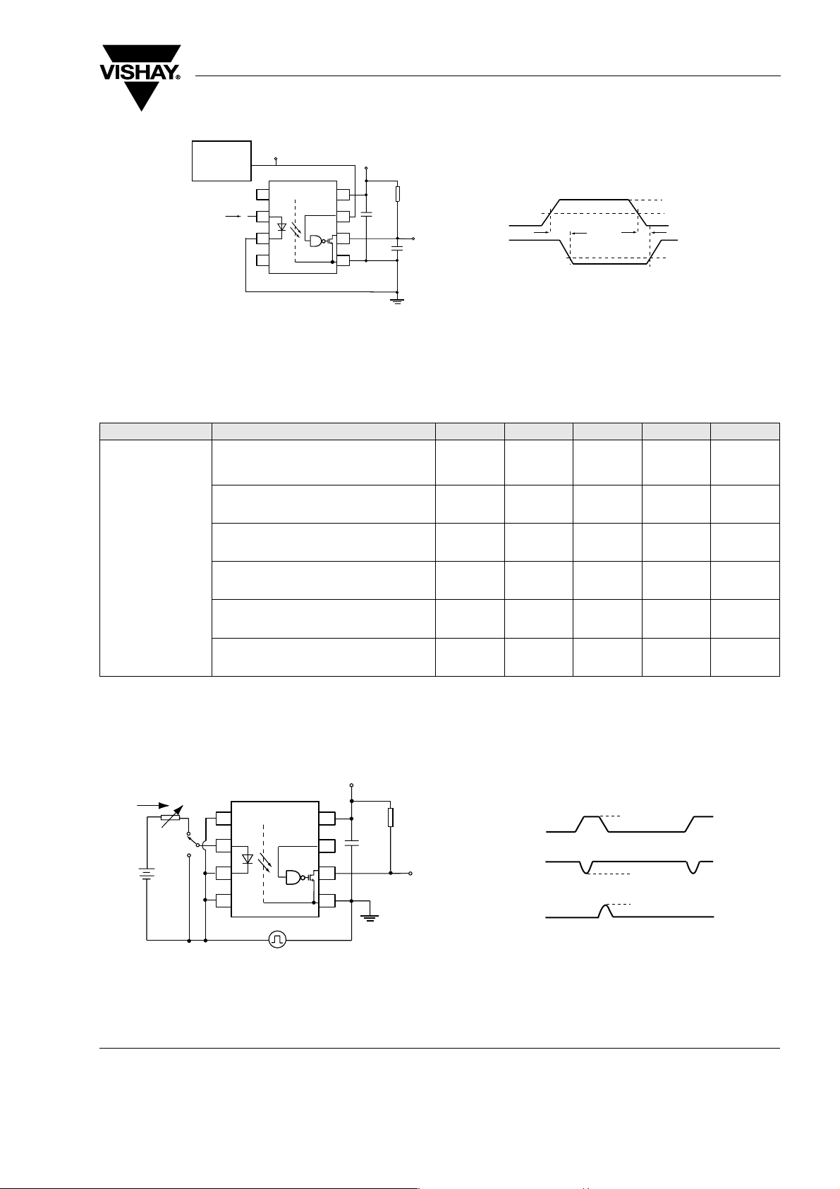
Pulse Gen.
Z=50Ω
o
t =t =5ns
r
f
InputI
F
Monitoring
Node
V
CC
V
CC
8
E
7
0.1 µF
Bypass
6
5
Single Channel
1
I
F
2
3
R
M
4
The Probe and Jig Capacitances are included in C
V
V
OUT
GND
Figure 1. Single Channel Test Circuit for t
Pulse Gen.
Z=50Ω
o
t =t =5ns
r
f
I
F
1
Input
Monitoring
Node
R
2
3
M
4
18963-2
R
L
OutputV
Monitoring
Node
C = 15 pF
L
L
Dual Channel
V
GND
O
CC
InputI
OutputV
8
7
6
5
F
O
PLH
0.1 µF
Bypass
, t
t
PHL
PHL
V
, tr and t
CC
R
L
=15pF
C
L
f
OutputV
O
Monitoring
Node
= 7.5 mA
I
F
= 3.75 mA
I
F
0mA
V
OH
1.5 V
V
OL
t
PL H
18964-2
www.vishay.com
4
Figure 2. Dual Channel Test Circuit for t
PLH
, t
PHL
, tr and t
f
Document Number 84732
Rev. 1.0, 07-Jun-05
Page 5
6N137 / VO2601 / 11 / VO2630 / 31 / VO4661
Vishay Semiconductors
Pulse Gen.
Z=50Ω
o
t =t =5ns
r
f
7.5 mA
I
F
The Probe and Jig Capacitances are includedinC
InputV
Monitoring Node
Single Channel
1
2
3
4
E
GND
V
OUT
V
CC
V
V
CC
0.1 µF
Bypass
R
L
OutputV
Monitoring
Node
C = 15 pF
L
O
L
InputV
OutputV
8
E
7
6
5
Figure 3. Single Channel Test Circuit for t
EHL
E
O
and t
t
EHL
ELH
t
ELH
18975-2
3V
1.5 V
1.5 V
Common Mode Transient Immunity
Parameter Test condition Symbol Min Ty p . Max Unit
|V
Common mode
transient immunity
(high)
1)
For 6N137 and VO2630
2)
For VO2601 and VO2631
3)
For VO2611 and VO4661
| = 10 V, VCC = 5 V, IF = 0 mA,
CM
= 2 V, RL = 350 Ω, T
V
O(min)
|V
| = 50 V, VCC = 5 V, IF = 0 mA,
CM
= 2 V, RL = 350 Ω, T
V
O(min)
| = 1 kV, VCC = 5 V, IF = 0 mA,
|V
CM
= 2 V, RL = 350 Ω, T
V
O(min)
| = 10 V, VCC = 5 V, IF = 7.5 mA,
|V
CM
= 0.8 V, RL = 350 Ω, T
V
O(max)
| = 50 V, VCC = 5 V, IF = 7.5 mA,
|V
CM
= 0.8 V, RL = 350 Ω, T
V
O(max)
| = 1 kV, VCC = 5 V, IF = 7.5 mA,
|V
CM
= 0.8 V, RL = 350 Ω, T
V
O(max)
amb
amb
amb
amb
amb
amb
= 25 °C
= 25 °C
= 25 °C
= 25 °C
= 25 °C
= 25 °C
| CMH |100 V/µs
1)
| CMH | 5000 10000 V/µs
2)
| CMH | 10000 15000 V/µs
3)
| CML |100 V/µs
1)
| CML | 5000 10000 V/µs
2)
| CML | 10000 15000 V/µs
3)
I
F
B
A
V
FF
Document Number 84732
Rev. 1.0, 07-Jun-05
V
CC
Single Channel
1
2
3
V
V
OUT
CC
V
8
E
7
6
0.1 µF
Bypass
R
L
OutputV
Monitoring
Node
V
CM
O
0V
Switch AT A: I 0 mA
V
5V
O
Switch AT A: 7.5 mA
4
+
Pulse Generator
Z=50Ω
O
GND
V
CM
-
5
V
V
0.5
O
Figure 4. Single Channel Test Circuit for Common Mode Transient Immunity
(PEAK)
V
CM
=
F
)
(min.
V
O
=
I
F
(max.)
V
O
18976-2
CM
CM
H
L
www.vishay.com
5
Page 6

6N137 / VO2601 / 11 / VO2630 / 31 / VO4661
Vishay Semiconductors
I
F
B
A
V
FF
18977-1
Figure 5. Dual Channel Test Circuit for Common Mode Transient Immunity
Safety and Insulation Ratings
As per IEC60747-5-2, §7.4.3.8.1, this optocoupler is suitable for "safe electrical insulation" only within the safety ratings. Compliance with
the safety ratings shall be ensured by means of protective circuits.
Parameter Test condition Symbol Min Ty p. Max Unit
Climatic Classification (according to
IEC 68 part 1)
Comparative Tracking Index CTI 175 399
V
IOTM
V
IORM
P
SO
I
SI
T
SI
Creepage standard DIP-8 7 mm
Clearance standard DIP-8 7 mm
Creepage 400mil DIP-8 8 mm
Clearance 400mil DIP-8 8 mm
Insulation thickness, reinforced rated per IEC60950 2.10.5.1 0.2 mm
Dual Channel
1
2
3
4
V
+
Pulse Generator
Z=50Ω
O
GND
CM
-
V
8
CC
7
6
5
+5V
R
L
OutputV
Monitoring
0.1 µF
Bypass
Node
8000 V
630 V
O
55/110/21
500 mW
300 mA
175 °C
www.vishay.com
6
Document Number 84732
Rev. 1.0, 07-Jun-05
Page 7

6N137 / VO2601 / 11 / VO2630 / 31 / VO4661
Vishay Semiconductors
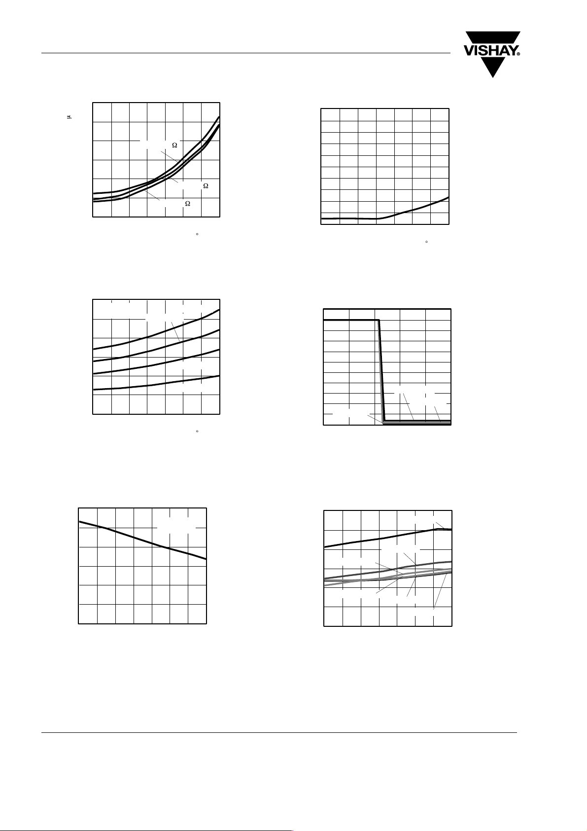
Typical Characteristics (Tamb = 25 °C unless otherwise specified)
4.0
1.7
1.6
1.5
1.4
1.3
1.2
F
V – Forward Voltage ( V )
1.1
1.0
17610
IF = 10 mA
–40 –20 0 20 40 60 80 100
T
amb
IF = 50 mA
IF = 1 mA
– Ambient Temperature ( °C )
IF = 20 mA
)
3.5
CCl
I – Low Level Supply Current ( mA
17614
3.0
2.5
2.0
1.5
1.0
0.5
0.0
VCC = 5 V
I
= 10 mA
F
–40 –20 0 20 40 60 80100
T
– Ambient Temperature ( C )
amb
VCC = 7 V
I
= 10 mA
F
Figure 6. Forward Voltage vs. Ambient Temperature
1.60
1.55
1.50
1.45
1.40
1.35
1.30
1.25
F
1.20
V – Forward Voltage ( V )
1.15
1.10
0 5 10 15 20 25 30 35 40 45 50
17611
– Forward Current ( mA )
I
F
Figure 7. Forward Voltage vs. Forward Current
7
6
)
5
4
3
2
R
1
I – Reverse Current ( nA
0
–40 –20 0 20 40 60 80 100
17613-1
T
– Ambient Temperature ( C )
amb
Figure 9. Low Level Supply Current vs. Ambient Temperature
3.5
)
3.4
3.3
3.2
3.1
3.0
2.9
CCh
2.8
I – High Level Supply Current ( mA
–40 –20 0 20 40 60 80100
17615
VCC = 5 V
I
= 0.25 mA
F
T
– Ambient Temperature ( C )
amb
VCC = 7 V
I
= 0.25 mA
F
Figure 10. High Level Supply Current vs. Ambient Temperature
2.8
2.7
2.6
2.5
2.4
2.3
2.2
th
2.1
I – Input Threshold ON Current ( A )
–40 –20 0 20 40 60 80100
T
amb
RL = 350
RL = 4 k
RL = 1 k
– Ambient Temperature ( C )17616
Figure 8. Reverse Current vs. Ambient Temperature
Document Number 84732
Rev. 1.0, 07-Jun-05
Figure 11. Input Threshold ON Current vs. Ambient Temperature
www.vishay.com
7
Page 8
6N137 / VO2601 / 11 / VO2630 / 31 / VO4661
Vishay Semiconductors
2.6
2.5
2.4
2.3
2.2
2.1
2.0
th
I – Input Threshold OFF Current ( A )
–40 –20 0 20 40 60 80100
17617
T
amb
RL = 350
RL = 4 k
RL = 1 k
– Ambient Temperature ( C )
Figure 12. Input Threshold OFF Current vs. Ambient Temperature
0.30
VCC = 5.5 V
I
= 5 mA
0.25
0.20
0.15
0.10
0.05
ol
V – Low Level Output Voltage ( V )
0.00
17618
F
–40 –20 0 20 40 60 80100
T
– Ambient Temperature ( C )
amb
IL = 16 mA
IL = 13 mA
IL = 10 mA
IL = 6 mA
50
45
40
35
30
25
20
15
10
5
oh
I – High Level Output Current ( nA )
0
–40 –20 0 20 40 60 80100
T
– Ambient Temperature ( C )17620
amb
Figure 15. High Level Output Current vs. Ambient Temperature
5.5
5.0
4.5
4.0
3.5
3.0
2.5
2.0
1.5
o
1.0
V – Output Voltage ( V )
0.5
RL = 4 kW
0.0
012345
17621
IF – Forward Input Current ( mA )
RL = 350 W
RL = 1 kW
Figure 13. Low Level Output Voltage vs. Ambient Temperature
60
50
IF = 5 mA
= 10 mA
I
F
40
30
20
10
ol
I – Low Level Output Current ( mA )
0
–40 –20 0 20 40 60 80 100
T
17619
– Ambient Temperature ( _C )
amb
Figure 14. Low Level Output Current vs. Ambient Temperature
www.vishay.com
8
Figure 16. Output Voltage vs. Forward Input Current
120
100
80
t
350 Ω
60
40
20
P
t – Propagation Delay time ( ns )
PLH,
t
350 Ω
PHL,
t
0
–40 –20 0 20 40 60 80 100
T
17622
– Ambient Temperature ( °C )
amb
t
PLH,
PHL,
1 kΩ
1 kΩ
t
PLH,
t
PHL,
4 kΩ
4 kΩ
Figure 17. Propagation Delay vs. Ambient Temperature
Document Number 84732
Rev. 1.0, 07-Jun-05
Page 9

6N137 / VO2601 / 11 / VO2630 / 31 / VO4661
Vishay Semiconductors
120
t
PLH,
4 kΩ
100
80
t
350 Ω
PLH,
60
40
t
PHL,
20
P
t – Propagation Delay time ( ns )
0
350 Ω
t
t
PLH,
PHL,
1 kΩ
1 kΩ
t
PHL,
4 kΩ
5 7 9 11 13 15
17623
IF – Forward Current ( mA )
Figure 18. Propagation Delay vs. Forward Current
50
40
30
20
10
PWD – Pulse Width Distortion ( ns )
0
–40 –20 0 20 40 60 80100
17624
T
– Ambient Temperature ( °C )
amb
RL = 4 kΩ
RL = 1 kΩ
RL = 350 Ω
300
tr, RL = 4 kΩ
250
200
150
100
50
r,f
t – Rise and Fall Time ( ns )
tr, RL = 1 kΩ
tr, RL = 350 Ω
tf, RL = 350 Ω
tf, RL = 1 kΩ
tf, RL = 4 kΩ
0
–40 –20 0 20 40 60 80 100
T
17626
– Ambient Temperature ( °C )
amb
Figure 21. Rise and Fall Time vs. Ambient Temperature
300
tr, RL = 4 kΩ
250
200
150
100
tr, RL = 1 kΩ
50
r,f
t – Rise and Fall Time ( ns )
tr, RL = 350 Ω
0
5 7 9 11 13 15
17627
tf, RL = 350 Ω
tf, RL = 1 kΩ
tf, RL = 4 kΩ
IF – Forward Current ( mA )
Figure 19. Pulse Width Distortion vs. Ambient Temperature
60
50
RL = 4 kΩ
40
30
20
RL = 1 kΩ
10
PWD – Pulse Width Distortion ( ns )
0
RL = 350 Ω
5 7 9 11 13 15
17625
– Forward Current ( mA )
I
F
Figure 20. Pulse Width Distortion vs. Forward Current
Document Number 84732
Rev. 1.0, 07-Jun-05
Figure 22. Rise and Fall Time vs. Forward Current
60
50
t
= 4 kΩ
t
eHL
eLH
t
= 350 Ω
eLH
= 350 Ω
t
= 4 kΩ
eHL
40
30
t
= 1 kΩ
eLH
20
10
t
= 1 kΩ
e
t – Enable Propagation Delay ( ns )
17628
eHL
0
–40 –20 0 20 40 60 80100
T
– Ambient Temperature ( °C )
amb
Figure 23. Enable Propagation Delay vs. Ambient Temperature
www.vishay.com
9
Page 10

6N137 / VO2601 / 11 / VO2630 / 31 / VO4661
Vishay Semiconductors
Package Dimensions in Inches (mm)
pin one ID
i178006
.255 (6.48)
.268 (6.81)
.030 (0.76)
.045 (1.14)
4° typ.
.050 (1.27)
.018 (.46)
.022 (.56)
Option 6
.407 (10.36)
.391 (9.96)
.307 (7.8)
.291 (7.4)
4
3
5
6
.379 (9.63)
.390 (9.91)
.100 (2.54) typ.
1
2
7 8
.031 (0.79)
.130(3.30)
.150 (3.81)
.020 (.51 )
.035(.89)
Option 7
.300 (7.62)
TYP.
ISO Method A
.300 (7.62)
typ.
10°
3°–9°
.008 (.20)
.012 (.30)
.110 (2.79)
.130(3.30)
.230(5.84)
.250(6.35)
www.vishay.com
10
.014 (0.35)
.010 (0.25)
.400 (10.16)
.430 (10.92)
.028 (0.7)
MIN.
.315 (8.0)
MIN.
.331 (8.4)
MIN.
.406 (10.3)
MAX.
.180 (4.6)
.160 (4.1)
18450-1
Document Number 84732
Rev. 1.0, 07-Jun-05
Page 11

6N137 / VO2601 / 11 / VO2630 / 31 / VO4661
Vishay Semiconductors
Ozone Depleting Substances Policy Statement
It is the policy of Vishay Semiconductor GmbH to
1. Meet all present and future national and international statutory requirements.
2. Regularly and continuously improve the performance of our products, processes, distribution and operating
systems with respect to their impact on the health and safety of our employees and the public, as well as
their impact on the environment.
It is particular concern to control or eliminate releases of those substances into the atmosphere which are
known as ozone depleting substances (ODSs).
The Montreal Protocol (1987) and its London Amendments (1990) intend to severely restrict the use of ODSs
and forbid their use within the next ten years. Various national and international initiatives are pressing for an
earlier ban on these substances.
Vishay Semiconductor GmbH has been able to use its policy of continuous improvements to eliminate the use
of ODSs listed in the following documents.
1. Annex A, B and list of transitional substances of the Montreal Protocol and the London Amendments
respectively
2. Class I and II ozone depleting substances in the Clean Air Act Amendments of 1990 by the Environmental
Protection Agency (EPA) in the USA
3. Council Decision 88/540/EEC and 91/690/EEC Annex A, B and C (transitional substances) respectively.
Vishay Semiconductor GmbH can certify that our semiconductors are not manufactured with ozone depleting
substances and do not contain such substances.
We reserve the right to make changes to improve technical design
and may do so without further notice.
Parameters can vary in different applications. All operating parameters must be validated for each
customer application by the customer. Should the buyer use Vishay Semiconductors products for any
unintended or unauthorized application, the buyer shall indemnify Vishay Semiconductors against all
claims, costs, damages, and expenses, arising out of, directly or indirectly, any claim of personal
damage, injury or death associated with such unintended or unauthorized use.
Vishay Semiconductor GmbH, P.O.B. 3535, D-74025 Heilbronn, Germany
Document Number 84732
Rev. 1.0, 07-Jun-05
www.vishay.com
11
Page 12

Legal Disclaimer Notice
Vishay
Document Number: 91000 www.vishay.com
Revision: 08-Apr-05 1
Notice
Specifications of the products displayed herein are subject to change without notice. Vishay Intertechnology, Inc.,
or anyone on its behalf, assumes no responsibility or liability for any errors or inaccuracies.
Information contained herein is intended to provide a product description only. No license, express or implied, by
estoppel or otherwise, to any intellectual property rights is granted by this document. Except as provided in Vishay's
terms and conditions of sale for such products, Vishay assumes no liability whatsoever, and disclaims any express
or implied warranty, relating to sale and/or use of Vishay products including liability or warranties relating to fitness
for a particular purpose, merchantability, or infringement of any patent, copyright, or other intellectual property right.
The products shown herein are not designed for use in medical, life-saving, or life-sustaining applications.
Customers using or selling these products for use in such applications do so at their own risk and agree to fully
indemnify Vishay for any damages resulting from such improper use or sale.
 Loading...