

Page 1
查询592D105X-035A2-15H供应商
592D
Vishay Sprague
Solid Tantalum Chip Capacitors
TANTAMOUNT®, Low Profile, Conformal Coated, Maximum CV
FEATURES
• New extended range offerings.
• 1.0mm to 2.5mm height.
• Terminations: Lead (Pb)-free (2) standard.
• Low Impedance
• 8mm, 12mm and 24mm tape and reel packaging
available per EIA-481-1 and reeling per IEC 286-3. 7”
[178mm] standard.
13” [330mm] available.
• Case code compatibility with EIA 535BAAC and
CECC 30801 molded chips.
PERFORMANCE CHARACTERISTICS
Operating Temperature: - 55°C to + 85°C. (To + 125°C
with voltage derating.)
ORDERING INFORMATION
592D
TYPE
This is expressed in
picofarads. The first two
digits are the significant
figures. The third is the
number of zeros to follow.
Note: Preferred Tolerance and reel sizes are in bold.
We reserve the right to supply higher voltage ratings and tighter capacitance tolerance capacitors in the same case size.
Voltage substitutions will be marked with the higher voltage rating.
106
CAPACITANCE
X0
CAPACITANCE
TOLERANCE
X0 = ± 20%
X9 = ± 10%
010
DC VOLTAGE RATING
@ + 85°C
This is expressed in volts. To
complete the three-digit block,
zeros precede the voltage rating.
A decimal point is indicated by
an "R" (6R3 = 6.3 volts).
Capacitance Range: 1.0µF to 3300µF
Capacitance Tolerance: ±10%, ±20% standard.
Voltage Rating: 4 WVDC to 35 WVDC
B
CASE CODE
See Ratings
and Case
Codes Table.
2
TERMINATION
2 = 100% Tin
4 = Gold Plated
T=Tape and Reel
W = 13” [330mm] Reel
T
REEL SIZE AND
PACKAGING
7" [178mm] Reel
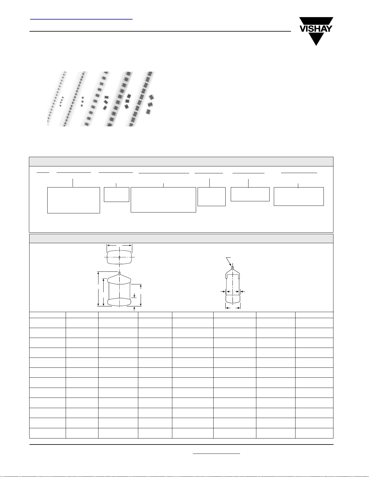
DIMENSIONS in inches [millimeters]
W
Tantalum Wire Nib
Identifies Anode
(+) Terminal
L
D
CASE CODE L (Max.) W H A B D (Ref.) J (Max.)
A
B
C
D
R
S
T
U
V
W
X
Y
Note: The anode termination (D less B) will be a minimum of 0.012" [0.3mm].
0.146 0.072 ± 0.012 0.048 ± 0.012 0.031 ± 0.012 0.087 ± 0.016 0.115 0.004
[3.7] [1.8 ± 0.3] [1.2 ± 0.3] [0.80 ± 0.30] [2.2 ± 0.4] [2.9] [0.1]
0.158
[4.0] [2.8 + 0.3-0.4] [1.2 ± 0.3] [0.80 ± 0.30] [2.5 ± 0.4] [3.5] [0.1]
0.281 0.126 ± 0.012 0.047 ± 0.012 0.051 ± 0.012 0.180 ± 0.024 0.238 0.004
[7.1] [3.2 ± 0.3] [1.2 ± 0.3] [1.3 ± 0.30] [4.4 ± 0.6] [6.0] [0.1]
0.298 0.170 ± 0.012 0.047 ± 0.012 0.051 ± 0.012 0.180 ± 0.024 0.254 0.004
[7.5] [4.3 ± 0.3] [1.2 ± 0.3] [1.3 ± 0.30] [4.6 ± 0.6] [6.4] [0.1]
0.285 0.235 ± 0.012 0.047 ± 0.012 0.051 ± 0.012 0.180 ± 0.024 0.246 0.004
[7.2] [6.0 ± 0.3] [1.2 ± 0.3] [1.3 ± 0.30] [4.6 ± 0.6] [6.2] [0.1]
0.126 ± 0.012 0.063 ± 0.012 0.040 ± 0.012 0.031 ± 0.012 0.079 ± 0.012 0.087 0.004
[3.2 ± 0.3] [1.6 ± 0.3] [1.0 ± 0.3] [0.8 ± 0.3] [2.0 ± 0.3] [2.2] [0.1]
0.158 0.116 ± 0.012 0.079 0.031 ± 0.012 0.097 ± 0.016 0.139 0.004
[4.0] [2.8 ± 0.3] [2.0] Max. [0.8 ± 0.3] [2.5 ± 0.4] [3.5] [0.1]
0.281 0.126 ± 0.012 0.079 0.051 ± 0.012 0.180 ± 0.024 0.238 0.004
[7.1] [3.2 ± 0.3] [2.0] Max. [1.3 ± 0.3] [4.6 ± 0.6] [6.0] [0.1]
0.298 0.170 ± 0.012 0.079 0.051 ± 0.012 0.180 ± 0.024 0.254 0.004
[7.5] [4.3 ± 0.3] [2.0] Max. [1.3 ± 0.3] [4.6 ± 0.6] [6.4] [0.1]
0.285 0.235 ± 0.012 0.079 0.051 ± 0.012 0.180 ± 0.024 0.246 0.004
[7.2] [6.0 ± 0.3] [2.0] Max. [1.3 ± 0.3] [4.6 ± 0.6] [6.2] [0.1]
0.575 0.290 ± 0.010 0.079 0.050 ± 0.016 0.470 ± 0.024 0.524 0.004
[14.5] [7.37 ± 0.25] [2.0] Max. [1.3 ± 0.4] [11.9 ± 0.6] [13.2] [0.1]
0.575 0.290 ± 0.010 0.098 0.051 ± 0.016 0.470 ± 0.024 0.524 0.004
[14.5] [7.37 ± 0.25] [2.5] Max. [1.3 ± 0.4] [11.9 ± 0.6] [13.2] [0.1]
0.110 + 0.012-0.016
B
A
0.047 ± 0.012 0.031 ± 0.012 0.097 ± 0.016 0.139 0.004
J
J
H
www.vishay.com
74
For technical questions, contact tantalum@vishay.com
Document Number 40004
Revision 20-Oct-04
Page 2
592D
Vishay Sprague
RATINGS AND CASE CODES
µF 4 V 6.3 V 10 V 16 V 20 V 25 V 35 V
STD EXT STD EXT STD EXT STD EXT STD EXT STD EXT STD EXT
1 BA
1.5 B
2.2 BACB*
3.3 CBDC
4.7 ABAC R
6.8 B A C B D C R D
10 B A C B D B R B/D R
15 B A D B* R C U* R
22 B A A/B C B D/T C R/U*/T D U*/V*
33 B B/C A/S D/T* C R/T C/D V* R
47 C B* C/D A/B R/T D U R/T*
68 D B/C D/T/R B/C D/R/U* C/T V C*
100 R/T C/D D/R B/C/T D/U R V C*/D/U
150 D/R C/T D/U R V U W
220 U/V R V D/R/U D V/W W
330 V R/U W R/U/V V W
470 W D/U/V V/U/W
680 V/W W
1000 W X/W
1500 X X/Y
2200 X/Y X/Y*
3300 Y
* Contact factory for availability
STANDARD / EXTENDED RATINGS
CAPACITANCE
(µF)
22 A 592D226X_004A2T 0.9 6 2.40 0.16
22 B 592D226X_004B2T 0.9 6 1.60 0.22
33 B 592D336X_004B2T 1.3 6 1.60 0.22
47* B* 592D476X_004B2T* 1.9* 6* 1.5* 0.23*
47 C 592D476X_004C2T 1.9 6 0.40 0.5
68 B 592D686X_004B2T 2.7 6 1.40 0.24
68 C 592D686X_004C2T 2.7 6 0.35 0.53
68 D 592D686X_004D2T 2.7 6 0.27 0.68
100 C 592D107X_004C2T 4 8 0.35 0.53
100 D 592D107X_004D2T 4 8 0.26 0.69
100 R 592D107X_004R2T 4 8 0.20 0.87
100 T 592D107X_004T2T 4 8 0.45 0.42
150 C 592D157X_004C2T 6 8 0.36 0.52
150 D 592D157X_004D2T 6 8 0.25 0.71
150 R 592D157X_004R2T 6 8 0.20 0.87
150 T 592D157X_004T2T 6 8 0.45 0.42
220 R 592D227X_004R2T 8.3 8 0.20 0.87
220 V 592D227X_004V2T 8.3 8 0.20 0.78
220 U 592D227X_004U2T 8.3 8 0.19 0.76
330 R 592D337X_004R2T 13.2 8 0.18 0.91
330 U 592D337X_004U2T 13.2 8 0.15 0.86
330 V 592D337X_004V2T 13.2 8 0.12 1.08
470 D 592D477X_004D2T 18.8 8 0.14 0.94
470 U 592D477X_004U2T 18.8 8 0.10 1.05
470 V 592D477X_004V2T 18.8 8 0.10 1.18
470 W 592D477X_004W2T 18.8 10 0.10 1.32
680 V 592D687X_004V2T 27.2 12 0.10 1.18
680 W 592D687X_004W2T 27.2 12 0.10 1.32
1000 W 592D108X_004W2T 40 14 0.200 0.94
1500 X 592D158X_004X2T 60 20 0.04 2.1
2200 Y 592D228X_004Y2T 88 25 0.04 2.3
2200 X 592D228X_004X2T 88 25 0.55 2.3
*Preliminary values, contact factory for availability. For 10% tolerance, specify "9"; for 20% tolerance, change to "0". Extended range ratings are in bold print.
CASE
CODE PART NUMBER
4 WVDC @ + 85°C, SURGE = 5.2 V . . . 2.7 WVDC @ + 125°C, SURGE = 3.4 V
Max. DCL
@ + 25°C
(µA)
Max. DF
@ + 25°C
120 Hz
(%)
Max. ESR
@ + 25°C
100kHz
(Ohms)
Max. RIPPLE
100kHz
Irms
(Amps)
Document Number 40004
Revision 20-Oct-04
For technical questions, contact tantalum@vishay.com
www.vishay.com
75
Page 3
592D
Vishay Sprague
STANDARD / EXTENDED RATINGS
CAPACITANCE
(µF)
15 A 592D156X_6R3A2T 0.9 6 2.50 0.15
15 B 592D156X_6R3B2T 0.9 6 1.70 0.22
22 A 592D226X_6R3A2T 1.4 6 1.5 0.23
22 A 592D226X_6R3A2T13H** 1.4 6 1.5 0.2
22 B 592D226X_6R3B2T 1.4 6 1.5 0.23
33 A 592D336X_6R3A2T 2.1 6 1.70 0.32
33 B 592D336X_6R3B2T 2.1 6 1.40 0.24
33 C 592D336X_6R3C2T 2.1 6 0.40 0.5
33 S 592D336X_6R3S2T 2.1 8 1.3 0.28
33 S 592D336X_6R3S2T12H** 2.1 10 2.0 0.17
47 A 592D476X_6R3A2T 3 8 1.40 0.21
47 B 592D476X_6R3B2T 3 8 1.40 0.21
47 C 592D476X_6R3C2T 3 6 0.40 0.5
47 D 592D476X_6R3D2T 3 6 0.30 0.65
68 B 592D686X_6R3B2T 4.3 6 0.38 0.46
68 B 592D686X_6R3B2T13H** 4.3 8 0.60 0.36
68 C 592D686X_6R3C2T 4.3 6 0.38 0.51
68 D 592D686X_6R3D2T 4.3 6 0.27 0.68
68 R 592D686X_6R3R2T 4.3 6 0.20 0.87
68 T 592D686X_6R3T2T 4.3 6 0.50 0.4
100 B 592D107X_6R3B2T15H** 6.3 10 1.0 0.28
100 C 592D107X_6R3C2T 6.3 8 0.38 0.51
100 D 592D107X_6R3D2T 6.3 8 0.26 0.69
100 R 592D107X_6R3R2T 6.3 8 0.20 0.87
100 T 592D107X_6R3T2T 6.3 8 0.45 0.42
150 D 592D157X_6R3D2T 9.5 8 0.25 0.71
150 R 592D157X_6R3R2T 9.5 8 0.20 0.87
150 U 592D157X_6R3U2T 9.5 8 0.19 0.76
220 D 592D227X_6R3D2T 13.9 8 0.22 0.75
220 R 592D227X_6R3R2T 13.9 8 0.18 0.91
220 U 592D227X_6R3U2T 13.9 8 0.15 0.86
220 V 592D227X_6R3V2T 13.9 8 0.12 1.08
330 C 592D337X_6R3C2T16H** 20.8 10 0.15 0.81
330 R 592D337X_6R3R2T 20.8 8 0.18 0.91
330 U 592D337X_6R3U2T 20.8 8 0.10 1.05
330 V 592D337X_6R3V2T 20.8 8 0.10 1.18
330 W 592D337X_6R3W2T 20.8 8 0.10 1.32
470 U 592D477X_6R3U2T 29.6 14 0.10 1.05
470 V 592D477X_6R3V2T 29.6 10 0.10 1.18
470 W 592D477X_6R3W2T 29.6 10 0.10 1.32
680 R 592D687X_6R3R2T16H** 42.8 14 0.13 1.16
680 W 592D687X_6R3W2T 42.8 10 0.100 1.32
1000 W 592D108X_6R3W2T 63 20 0.2 0.94
1000 X 592D108X_6R3X2T 63 16 0.04 2.1
1500 Y 592D158X_6R3Y2T 95 20 0.035 2.3
1500 X 592D158X_6R3X2T 95 25 0.045 1.97
2200* Y* 592D228X_6R3Y2T* 139* 35* 0.055* 1.80*
2200 X 592D228X_6R3X2T 139 35 0.055 1.80
3300 Y 592D338X_6R3Y2T 208 35 0.055 1.80
10 A 592D106X_010A2T 1 6 2.60 0.15
10 B 592D106X_010B2T 1 6 1.70 0.22
22 B 592D226X_010B2T 2.2 6 1.50 0.23
22 C 592D226X_010C2T 2.2 6 0.40 0.50
33 C 592D336X_010C2T 3.3 6 0.40 0.50
33 D 592D336X_010D2T 3.3 6 0.30 0.65
33* T* 592D336X_010T2T* 3.3* 6* 0.50* 0.40*
47 D 592D476X_010D2T 4.7 6 0.27 0.68
47 R 592D476X_010R2T 4.7 6 0.20 0.87
47 T 592D476X_010T2T 4.7 6 0.50 0.40
68 C 592D686X_010C2T 6.8 6 0.14 0.84
68 D 592D686X_010D2T 6.8 6 0.27 0.68
68 R 592D686X_010R2T 6.8 6 0.20 0.87
68 T 592D686X_010T2T 6.8 6 0.45 0.42
68* U* 592D686X_010U2T* 6.8* 6* 0.25* 0.66*
100 D 592D107X_010D2T 10 8 0.10 1.11
100 U 592D107X_010U2T 10 8 0.19 0.76
100 R 592D107X_010R2T 10.0 8 0.22 0.83
150 U 592D157X_010U2T 15 8 0.17 0.80
150 V 592D157X_010V2T 15 8 0.14 1.00
220 V 592D227X_010V2T 22 8 0.12 1.08
220 W 592D227X_010W2T 22 8 0.10 1.32
330* V* 592D337X_010V2T* 33* 8* 0.10* 1.18*
330 W 592D337X_010W2T 33 8 0.10 1.32
** xyH indicates maximum height in (mm), i.e., 1.5 max (H) = 15Hmm
*Preliminary values, contact factory for availability. For 10% tolerance, specify "9"; for 20% tolerance, change to "0". Extended range ratings are in bold print.
*Voltage range under development.
CASE
CODE PART NUMBER
6.3 WVDC @ + 85°C, SURGE = 8 V . . . 4 WVDC @ + 125°C, SURGE = 5 V
10 WVDC @ + 85°C, SURGE = 13 V . . . 7 WVDC @ + 125°C, SURGE = 8 V
Max. DCL
@ + 25°C
(µA)
Max. DF
@ + 25°C
120 Hz
(%)
Max. ESR
@ + 25°C
100kHz
(Ohms)
Max. RIPPLE
100kHz
Irms
(Amps)
www.vishay.com
76
For technical questions, contact tantalum@vishay.com
Document Number 40004
Revision 20-Oct-04
Page 4
592D
Vishay Sprague
STANDARD / EXTENDED RATINGS
CAPACITANCE
(µF)
4.7 A 592D475X_016A2T 0.8 6 3.50 0.13
6.8 A 592D685X_016A2T 1.1 6 3.50 0.13
6.8 B 592D685X_016B2T 1.1 6 1.80 0.21
10 B 592D106X_016B2T 1.6 6 1.60 0.22
10 C 592D106X_016C2T 1.6 6 1.00 0.32
15* B* 592D156X_016B2T* 2.4* 6* 1.4* 0.24*
15 D 592D156X_016D2T 2.4 6 0.50 0.50
22 C 592D226X_016C2T 3.5 6 0.50 0.46
22 D 592D226X_016D2T 3.5 6 0.40 0.60
22 T 592D226X_016T2T 3.5 6 0.6 0.36
33 C 592D336X_016C2T 5.3 6 0.25 0.66
33 D 592D336X_016D2T 5.3 6 0.30 0.62
33 R 592D336X_016R2T 5.3 6 0.27 0.75
33 T 592D336X_016T2T 5.3 6 0.6 0.36
47 R 592D476X_016R2T 7.5 6 0.25 0.77
47 T 592D476X_016T2T 7.5 6 0.45 0.42
47 U 592D476X_016U2T 7.5 6 0.25 0.66
68* C* 592D686X_016C2T* 10.9* 6* 0.50* 1.20*
68 U 592D686X_016U2T 10.9 6 0.25 0.66
68 V 592D686X_016V2T 10.9 6 0.17 0.91
100* C* 592D107X_016C2T* 16* 8* 0.30* 1.80*
100 D 592D107X_016D2T 16 8 0.15 0.97
100 U 592D107X_016U2T 16 8 0.15 0.97
100 V 592D107X_016V2T 16 8 0.15 0.97
150 W 592D157X_016W2T 24 8 0.1 1.32
220 W 592D227X_016W2T 35.2 8 0.2 0.94
4.7 A 592D475X_020A2T 0.9 6 3.80 0.13
4.7 B 592D475X_020B2T 0.9 6 3.20 0.16
6.8 B 592D685X_020B2T 1.4 6 3.10 0.16
6.8 C 592D685X_020C2T 1.4 6 1.10 0.30
10 B 592D106X_020B2T 2 6 3.00 0.16
10 D 592D106X_020D2T 2 6 0.50 0.48
15 C 592D156X 020C2T 3 6 0.60 0.42
15 R 592D156X_020R2T 3 6 0.40 0.65
22 D 592D226X_020D2T 4.4 6 0.40 0.56
22 R 592D226X_020R2T 4.4 6 0.28 0.73
22 T 592D226X_020T2T 4.4 6 0.60 0.37
22* U* 592D226X_020U2T* 4.4* 6* 0.30* 0.61*
33 R 592D336X_020R2T 6.6 6 0.28 0.73
33* V* 592D336X_020V2T* 6.6* 6* 0.26* 0.73*
2.2 A 592D225X_025A2T 0.6 6 8.00 0.09
2.2 B 592D225X_025B2T 0.6 6 6.00 0.12
3.3 B 592D335X_025B2T 0.8 6 5.60 0.12
3.3 C 592D335X_025C2T 0.8 6 2.00 0.22
4.7 C 592D475X_025C2T 1.2 6 1.60 0.25
6.8 C 592D685X_025C2T 1.7 6 1.50 0.26
6.8 D 592D685X_025D2T 1.7 6 1.30 0.31
10 B 592D106X_025B2T 2.5 6 2.00 0.115
10 D 592D106X_025D2T 2.5 6 1.20 0.32
10 R 592D106X_025R2T 2.5 6 0.48 0.56
15 R 592D156X_025R2T 3.8 6 0.40 0.61
15* U* 592D156X_025U2T* 3.8* 6* 0.40* 0.52*
22* U* 592D226X_025U2T* 5.5* 6* 0.30* 0.68*
22* V* 592D226X_025V2T* 5.5* 6* 0.30* 0.68*
*Preliminary values, contact factory for availability. For 10% tolerance, specify "9"; for 20% tolerance, change to "0". Extended range ratings are in bold print.
*Voltage range under development.
CASE
CODE PART NUMBER
16 WVDC @ + 85°C, SURGE = 20 V . . . 10 WVDC @ + 125°C, SURGE = 12 V
20 WVDC @ + 85°C, SURGE = 26 V . . . 13 WVDC @ + 125°C, SURGE = 16 V
25 WVDC @ + 85°C, SURGE = 33 V . . . 17 WVDC @ + 125°C, SURGE = 20 V
Max. DCL
@ + 25°C
(µA)
Max. DF
@ + 25°C
120 Hz
(%)
Max. ESR
@ + 25°C
100kHz
(Ohms)
Max. RIPPLE
100kHz
Irms
(Amps)
Document Number 40004
Revision 20-Oct-04
For technical questions, contact tantalum@vishay.com
www.vishay.com
77
Page 5

592D
Vishay Sprague
STANDARD / EXTENDED RATINGS
CAPACITANCE
(µF)
CASE
CODE PART NUMBER
Max. DCL
@ + 25°C
(µA)
35 WVDC @ + 85°C, SURGE = 46 V . . . 23 WVDC @ + 125°C, SURGE = 28 V
1A592D105X_035A2T 0.5 4 10.0 0.08
1B592D105X_035B2T 0.5 4 6.50 0.11
1.5 B 592D155X_035B2T 0.5 4 4.2 0.14
2.2* B* 592D225X_035B2T* 0.8* 6* 6.00* 0.12*
2.2 C 592D225X_035C2T 0.8 6 3.50 0.17
3.3 C 592D335X_035C2T 1.2 6 3.20 0.18
3.3 D 592D335X_035D2T 1.2 6 2.10 0.24
4.7 R 592 D475X_035R2T 1.6 6 1.30 0.34
6.8 D 592 D685X_035D2T 2.4 6 1.30 0.31
6.8 R 592D685X_035R2T 2.4 6 1.20 0.35
10 R 592D106X_035R2T 3.5 6 1.20 0.35
TYPICAL CURVES OF ESR - AS A FUNCTION OF FREQUENCY
Max. DF
@ + 25°C
120 Hz
(%)
Max. ESR
@ + 25°C
100kHz
(Ohms)
Max. RIPPLE
100kHz
Irms
(Amps)
"A" Case
1000
100
OHMS
1µF, 35
10
15µF, 6.3
1
100 1K 10K 100K 1M
0.1
1000
100
10
OHMS
FREQUENCY IN HERTZ
"C" Case
IMPEDANCE
ESR
IMPEDANCE
ESR
4.7µF, 25 V
"B" Case
1000
100
OHMS
10
1
100 1K 10K 100K
10µF, 10 V
FREQUENCY IN HERTZ
IMPEDANCE
4.7µF, 20 V
"D" Case
100
10
OHMS
1
IMPEDANCE
ESR
ESR
6.8µF, 25 V
1
33µF, 6.3 V
0.1
100 1K 10K 100K 1M
www.vishay.com
FREQUENCY IN HERTZ
For technical questions, contact tantalum@vishay.com
78
0.1
47µF, 6.3 V
0.01
100 1K 10K 100K 1M
FREQUENCY IN HERTZ
Document Number 40004
Revision 20-Oct-04
Page 6

TYPICAL CURVES @ + 25°C, IMPEDANCE AND ESR VS FREQUENCY
592D
Vishay Sprague
"R" Case
100
10
IMPEDANCE
ESR
1
OHMS
10µF, 25 V
0.1
100µF, 6.3 V
0.01
100 1K 10K 100K 1M
592D 1500-4V X CASE ESR/IMPEDANCE VS FREQUENCY
10
1
FREQUENCY IN HERTZ
ESR
IMPEDANCE
"S" Case
100
10
1
OHMS
0.1
0.01
100 1000 10000 100000 1000000
592D 1500-6.3V Y CASE ESR/IMPEDANCE VS FREQUENCY
10.00
1.00
FREQUENCY IN HERTZ
IMPEDANCE
ESR
33 - 6.3V
ESR
IMPEDANCE
OHMS
0.1
0.01
100 1kHz 10kHz 100kHz 1MHz 10MHz
FREQUENCY (Hz)
592D 1000-6.3V X CASE ESR/IMPEDANCE VS FREQUENCY
10.00
ESR
IMPEDANCE
1.00
OHMS
0.10
0.01
100 1kHz 10kHz 100kHz 1MHz 10MHz
FREQUENCY (Hz)
OHMS
0.10
0.01
100 1kHz 10kHz 100kHz 1MHz 10MHz
FREQUENCY (Hz)
592D 2200-4V Y CASE ESR/IMPEDANCE VS FREQUENCY
10.00
ESR
IMPEDANCE
1.00
OHMS
0.10
0.01
100 1kHz 10kHz 100kHz 1MHz 10MHz
FREQUENCY (Hz)
Document Number 40004
Revision 20-Oct-04
For technical questions, contact tantalum@vishay.com
www.vishay.com
79
Page 7

592D
Vishay Sprague
PERFORMANCE CHARACTERISTICS
1. Operating Temperature: Capacitors are designed to
operate over the temperature range - 55°C to + 85°C.
1.1 Capacitors may be operated to + 125°C with
voltage derating to two-thirds the + 85°C rating.
+ 85°C Rating + 125°C Rating
Working
Voltage
(V)
4
6.3
10
16
20
25
35
Surge
Voltage
(V)
5.2
8
13
20
26
32
46
Working
Voltage
(V)
2.7
4
7
10
13
17
23
Surge
Voltage
(V)
3.4
5
8
12
16
20
28
2. DC Working Voltage: The DC working voltage is the
maximum operating voltage for continuous duty at the
rated temperature.
3. Surge Voltage: The surge DC rating is the maximum
voltage to which the capacitors may be subjected
under any conditions, including transients and peak
ripple at the highest line voltage. 592D228X_6R3X2T
and 592D338X_6R3V2T, not surge voltage tesed.
3.1 Surge Voltage Test: Capacitors shall withstand
the surge voltage applied in series with a 33 ohm
± 5% resistor at the rate of one-half minute on,
one-half minute off, at + 85°C, for 1000 successive
test cycles.
3.2 Following the surge voltage test, the dissipation
factor and the leakage current shall meet the initial
requirements; the capacitance shall not have changed
more than ± 10%.
4. Capacitance Tolerance: The capacitance of all
capacitors shall be within the specified tolerance
limits of the normal rating.
- 55°C
- 10%
+ 85°C
+ 10%
+ 125°C
+ 12%
6. Dissipation Factor: The dissipation factor,
determined from the expression 2πfRC, shall not
exceed values listed in the Standard Ratings Table.
6.1 Measurements shall be made by the bridge method
at, or referred to, a frequency of 120 Hz and a
temperature of + 25°C.
7. Leakage Current: Capacitors shall be stabilized at
the rated temperature for 30 minutes. Rated voltage
shall be applied to capacitors for 5 minutes using a
steady source of power (such as a regulated power
supply) with 1000 ohm resistor connected in series
with the capacitor under test to limit the charging
current. Leakage current shall then be measured.
Note that the leakage current varies with temperature
and applied voltage. See graph below for the
appropriate adjustment factor.
TYPICAL LEAKAGE CURRENT FACTOR RANGE
100
+ 125°C
10
1.0
+ 85°C
+ 55°C
+ 25°C
0°C
4.1 Capacitance measurements shall be made by means
of polarized capacitance bridge. The polarizing
voltage shall be of such magnitude that there shall be
no reversal of polarity due to the AC component. The
maximum voltage applied to capacitors during
measurement shall be 2 volts rms at 120 Hz at +25°C.
If the AC voltage applied is less than one-half volt rms,
no DC bias is required. Accuracy of the bridge shall
be within ± 2%.
5. Capacitance Change With Temperature: The
capacitance change with temperature shall not exceed
the following percentage of the capacitance measured
at + 25°C:
www.vishay.com
80
For technical questions, contact tantalum@vishay.com
0.1
Leakage Current Factor
0.01
0.001
0 10 20 30 40 50 60 70 80 90 100
- 55°C
Percent of Rated Voltage
Document Number 40004
Revision 20-Oct-04
Page 8

PERFORMANCE CHARACTERISTICS (Continued)
592D
Vishay Sprague
7.1 At + 25
°C, the leakage current shall not exceed
the value listed in the Standard Ratings Table.
7.2 At + 85
°C, the leakage current shall not exceed 10
times the value listed in the Standard Ratings Table.
7.3 At + 125
°C, the leakage current shall not exceed 12
times the value listed in the Standard Ratings Table.
8. Equivalent Series Resistance: Measurements shall
be made by the bridge method at, or referred to, a
frequency of 100 KHz and a temperature of + 25°C.
8.1 The Equivalent Series Resistance shall not exceed the
value listed in the Standard Ratings Table.
9. Life Test: Capacitors shall withstand rated DC
voltage applied at + 85°C for 2000 hours or derated
DC voltage applied at + 125°C for 1000 hours.
9.1 Following the life test, the dissipation factor and
leakage shall meet the initial requirement; the
capacitance change shall not exceed ± 10% of the
initial value.
10 Humidity Test: Capacitors shall withstand 1000 hours
at + 40°C, 90% to 95% relative humidity, with no
voltage applied
10.1 Following the humidity test, capacitance change shall
not exceed ± 10% of the initial value, dissipation factor
shall not exceed 150% of the initial requirement;
leakage currrent shall not exceed 200% of the initial
requirement at + 25°C
11. Solderability: Capacitors will meet the solderability
requirements of ANSI/J-STD-002, test B category 1.
12. Resistance to Soldering Heat: Capacitors mounted
on a substrate will withstand + 260°C for 5 seconds.
12.1 Following the resistance to soldering heat test,
capacitance, dissipation factor and DC leakage
current shall meet the initial requirement.
13. Marking: The small body area of these capacitors
does not allow elaborate marking schemes. All
required information is present on the carton or
package in which the parts are shipped; in addition,
part number, quantity and data code are indicated on
the reels.
14. Terminal Strength: Per IEC-384-3, minimum of
5N shear force.
15. Environmental: Mercury, CFC and ODS materials
are not used in the manufacture of these capacitors.
16. Flammability: Encapsulant materials meet UL94 V0
17. Capacitor Failure Mode: The predominant failure
mode for solid tantalum capacitors is increased
leakage current resulting in a shorted circuit. Capacitor failure may result from excess forward or reverse
DC voltage, surge current, ripple current, thermal
shock or excessive temperature.
The increase in leakage is caused by a breakdown of
the Ta
dielectric. For additional information on
2O5
leakage failure of solid tantalum chip capacitors, refer
to Vishay Sprague Technical Paper, “Leakage Failure
Mode in Solid Tantalum Chip Capacitors.”
GUIDE TO APPLICATION
1.0 Recommended rated working voltage guidelines:
(-55°C to + 85°C)
Application Voltage Recommended
2. A-C Ripple Current: The maximum allowable ripple
current shall be determined from the formula:
where,
P = Power Dissipation in Watts @ + 25°C as given
in the table in Paragraph Number 6.0 (
Document Number 40004
Revision 20-Oct-04
(V) Capacitor Voltage
2.5 4
4 6.3
58
610
10 16
12 20
18 25
24 35
Rating (V)
P
I
rms
R
=
ESR
Power Dissipation)
For technical questions, contact tantalum@vishay.com
R
= The capacitor Equivalent Series Resistance
ESR
at the specified frequency.
3. A-C Ripple Voltage: The maximum allowable ripple
voltage shall be determined from the formula:
V
= Z
rms
P
R
ESR
or, from the formula:
V
= I
where,
rms
rms
x Z
P = Power Dissipation in Watts @ + 25°C as given in
the table in Paragraph Number 6.0 (Power
Dissipation).
R
= The capacitor Equivalent Series Resistance
ESR
at the specified frequency.
Z = The capacitor impedance at the specified
frequency.
www.vishay.com
81
Page 9

592D
Vishay Sprague
GUIDE TO APPLICATION (Continued)
3.1 The sum of the peak AC voltage plus the applied DC
voltage shall not exceed the DC voltage rating of the
capacitor.
3.2 The sum of the negative peak AC voltage plus the
applied DC voltage shall not allow a voltage reversal
exceeding 10% of the DC working voltage at + 25°C.
4.0 Reverse Voltage: These capacitors are capable of
withstanding peak voltages in the reverse direction
equal to 10% of the DC rating or 1 volt maximum at
+25°C and 5% of the DC voltage rating or 0.5 volt
maximum at + 85°C.
5.0 Temperature Derating: If these capacitors are to be
operated at temperatures above + 25°C, the
permissible rms ripple current or voltage shall be
calculated using the derating factors as shown:
Temperature Derating Factor
+ 25°C
+ 85°C
+ 125°C
6.0 Power Dissipation: Power dissipation will be
affected by the heat sinking capability of the mounting
surface. Non-sinusoidal ripple current may produce
heating effects which differ from those shown. It is
important that the equivalent
Irms
established when calculating permissible operating
levels. (Power dissipation calculated using + 25°C
temperature rise.)
Maximum Permissible
Case Code
A
B
C
D
R
S
T
U
V
W
X
Y
Power Dissipation
@ + 25°C (Watts) in free air
7.0 Printed Circuit Board Materials: The capacitors are
compatible with most commonly used printed circuit
board materials (alumina substrates, FR4, FR5,
G10, PTFE-fluorocarbon and porcelanized steel). If
your desired board material is not shown there please
contact the Tantalum Marketing Department for
assistance in determining compatibility.
8. Attachment:
8.1 Solder Paste: The recommended thickness of the
solder paste after application is 0.007" ± .001"
[.178mm ± .025mm]. Care should be exercised in
selecting the solder paste. The metal purity should
be as high as practical. The flux (in the paste) must
be active enough to remove the oxides formed on the
metallization prior to the exposure to soldering heat.
8.2 Soldering: Capacitors can be attached by
conventional soldering techniques - convection,
infrared reflow, wave soldering and hot plate methods.
1.0
0.9
0.4
value be
0.060
0.080
0.100
0.125
0.150
0.060
0.080
0.110
0.140
0.175
0.175
0.180
The Soldering Profile chart shows typical recomended
time/temperature conditions for soldering. Attachment
with a soldering iron is not recommended due to the
difficulty of controlling temperature and time at
temperature. The soldering iron must never come in
contact with the capacitor.
RECOMMENDED REFLOW SOLDERING PROFILE
250
200
150
100
50
TEMPERATURE DEG. CENTIGRADE
0 50 100 150 200 250 300 350
TIME (SECONDS)
9.0 Recommended Mounting Pad Geometries: The
nib must have sufficient clearance to avoid electrical
contact with other components. The width dimension
indicated is the same as the maximum width of the
capacitor. This is to minimize lateral movement.
REFLOW SOLDER PADS*
in inches [millimeters]
CASE WIDTH PAD SEPARATION
CODE (A) METALIZATION (C)
A 0.082 0.085 0.050
B 0.120 0.065 0.065
C 0.130 0.080 0.120
D 0.180 0.080 0.145
R 2.45 0.090 0.145
S 0.067 0.032 0.043
T 0.120 0.065 0.065
U 0.136 0.090 0.120
V 0.180 0.090 0.145
W 0.245 0.090 0.145
X 0.310 0.120 0.360
Y 0.310 0.120 0.360
* Pads for B, C and D case codes are otherwise pad compatible with
* Type 293D, B, C and D case codes respectively.
10.0 Cleaning (Flux Removal) After Soldering: The
592D capacitors are compatible with all commonly
used solvents such as TES, TMS, Prelete, Chlorethane,
Terpene and aqueous cleaning media. Solvents
containing methylene chloride or other epoxy solvents
should be avoided since these will attack the epoxy
encapsulation material.
B
C
B
A
[2.1] [1.7] [1.3]
[3.5] [1.7] [1.7]
[3.5] [2.3] [3.1]
[4.6) [2.3] [3.7]
[8.3] [2.3] [3.7]
[1.7] [0.8] [1.1]
[3.5] [1.7] [1.7]
[3.5] [2.3] [3.1]
[4.6) [2.3] [3.7]
[8.3] [2.3] [3.7]
[7.9] [3.0] [9.2]
[7.9] [3.0] [9.2]
www.vishay.com
82
For technical questions, contact tantalum@vishay.com
Document Number 40004
Revision 20-Oct-04
Page 10

TAPE AND REEL PACKAGING in inches [millimeters]
Top
Cover
Tape
Thickness
592D
Vishay Sprague
Standard orientation is with the
cathode (-) nearest to the
sprocket holes per EIA-481-1
and IEC 286-3.
Carrier
Embossment
Bending Radius
(Note 2)
R
Min.
Units Per Reel
Case Code
Tape
Width
Component
Pitch
7" [178]
Reel
13" [330]
Reel
A 8mm 4mm 2500 10000
B 12mm 4mm 2000 8000
C 12mm 8mm 1000 4000
D 12mm 8mm 1000 4000
R 12mm 8mm 1000 4000
S 8mm 4mm 2500 10000
T 12mm 8mm 2000 8000
U 12mm 8mm 1000 4000
V 12mm 8mm 1000 4000
W 12mm 8mm 1000 2500
X 24mm 12mm 500
Y 24mm 12mm 500
Document Number 40004
Revision 20-Oct-04
For technical questions, contact tantalum@vishay.com
www.vishay.com
83
Page 11

592D
Vishay Sprague
TAPE AND REEL PACKAGING in inches [millimeters]
Note: Metric dimensions will govern. Dimensions in inches are rounded and for reference only.
T
2
.024
[0.600]
Max.
B
Max.
1
(Note 6)
For Tape Feeder
Reference only
including draft.
Concentric around B
(Note 5)
Max.
.004 [0.10]
Max.
0
K
0
Top
Cover
Tape
Deformation
Between
Embossments
Top
Cover
Tape
.059 + .004 - 0.0
[1.5 + 0.10 - 0.0]
Center Lines
of Cavity
USER DIRECTION OF FEED
A
0
.157 ± .004
[4.0 ± 0.10]
B
0
P
1
10 Pitches Cumulative
Tolerance on Tape
± 0.008 [0.200]
.079 ± .002
[2.0 ± 0.05]
Maximum
Cavity Size
(Note 1)
Cathode (-)
Embossment
.030 [0.75]
Min. (Note 3)
.030 [0.75]
Min. (Note 4)
D1 Min. For Components
.079 x .047 [2.0 x 1.2] and Larger.
(Note 5)
.069
[1.75 ± 0.10]
F
W
± .004
20°
Maximum
Component
Rotation
(Side or Front Sectional View)
Anode (+)
DIRECTION OF FEED
B
0
A
0
(Top View)
TAPE
SIZE
8mm
12mm
12mm
Double Pitch
24mm
20° Maximum
Component Rotation
Typical
Component
Cavity
Center Line
Typical
Component
Center Line
B1 (Max.)
(Note 6)
0.179
[4.55]
0.323
[8.2]
0.323
[8.2]
0.791
[20.1]
3.937 [100.0]
.039 [1.0]
Max.
Tape
.039 [1.0] Max.
9.843 [250.0]
Camber
Allowable Camber to be .039/3.937 [1/100]
Non-Cumulative Over 9.843 [250.0]
(Top View)
D1 (Min.)
(Note 5)
0.039
[1.0]
0.059
[1.5]
0.059
[1.5]
0.059
[1.5]
F
0.138 ± 0.002
[3.5 ± 0.05]
0.217 ± 0.002
[5.5 ± 0.05]
0.217 ± 0.002
[5.5 ± 0.05]
0.453 ± 0.04
[11.5 ± 0.03]
Tape and Reel Specifications: All case sizes are available
on plastic embossed tape per EIA-481-1. Tape reeling per
IEC 286-3 is also available. Standard reel diameter is 7"
[178mm]. 13" [330mm] reels are available and recommended
as the most cost effective packaging method.
The most efficient packaging quantities are full reel increments
on a given reel diameter. The quantities shown allow for the
sealed empty pockets required to be in conformance with
EIA-481-1. Reel size and packaging orientation must be
specified in the Vishay Sprague part number.
1
0.157 ± 0.004
[4.0 ± 0.10]
0.157 ± 0.004
[4.0 ± 0.10]
0.315 ± 0.004
[8.0 ± 0.10]
0.472 ± 0.004
[12.0 ± 0.10]
R (Min.)
(Note 2)P
0.984
[25.0]
1.181
[30.0]
1.181
[30.0]
1.181
[30.0]
T
(Max.)
0.098
[2.5]
0.256
[6.5]
0.256
[6.5]
0.103
[2.6]
2
0.315 + .012 - .004
[8.0 + 0.3 - 0.1]
0.472 ± 0.012
0.472 ± 0.012
0.945 ± 0.012
W
[12.0 ± 0.30]
[12.0 ± 0.30]
[24.0 ± 0.03]
A0 B0 K
(Note 1)
Notes:
1. A0B0K0 are determined by the maximum dimensions to the ends of the terminals extending from the component body and/or the body
dimensions of the component. The clearance between the ends of the terminals or body of the component to the sides and depth of the
cavity (A0B0K0) must be within .002" [0.05mm] minimum and .020" [0.50mm] maximum. The clearance allowed must also prevent
rotation of the component within the cavity of not more than 20 degrees.
2. Tape with components shall pass around radius "R" without damage. The minimum trailer length may require additional length to
provide R minimum for 12mm embossed tape for reels with hub diameters approaching N minimum.
3. This dimension is the flat area from the edge of the sprocket hole to either the outward deformation of the carrier tape between the
embossed cavities or to the edge of the cavity whichever is less.
4. This dimension is the flat area from the edge of the carrier tape opposite the sprocket holes to either the outward deformation of the
carrier tape between the embossed cavity or to the edge of the cavity whichever is less.
5. The embossment hole location shall be measured from the sprocket hole controlling the location of the embossment. Dimensions of
embossment location and hole location shall be applied independent of each other.
6. B1 dimension is a reference dimension for tape feeder clearance only.
0
www.vishay.com
84
For technical questions, contact tantalum@vishay.com
Document Number 40004
Revision 20-Oct-04
 Loading...