

Bulletin PD-20265 07/00
32CTQ030
32CTQ030S
32CTQ030-1
SCHOTTKY RECTIFIER
Major Ratings and Characteristics
Characteristics 32CTQ Units
I
Rectangular 30 A
F(AV)
waveform
V
RRM
I
@ tp = 5 µs sine 900 A
FSM
VF@ 15 Apk, TJ = 125°C 0.40 V
TJrange - 55 to 150 °C
30 V
32 Amp
I
= 30Amp
F(AV)
VR = 30V
Description/Features
The 32CTQ030 Schottky rectifier series has been optimized
for low reverse leakage at high temperature. The proprietary
barrier technology allows for reliable operation up to 150° C
junction temperature. Typical applications are in switching
power supplies, converters, free-wheeling diodes, and reverse battery protection.
150° C TJ operation
High purity, high temperature epoxy encapsulation for
enhanced mechanical strength and moisture resistance
Low forward voltage drop
High frequency operation
Guard ring for enhanced ruggedness and long term
reliability
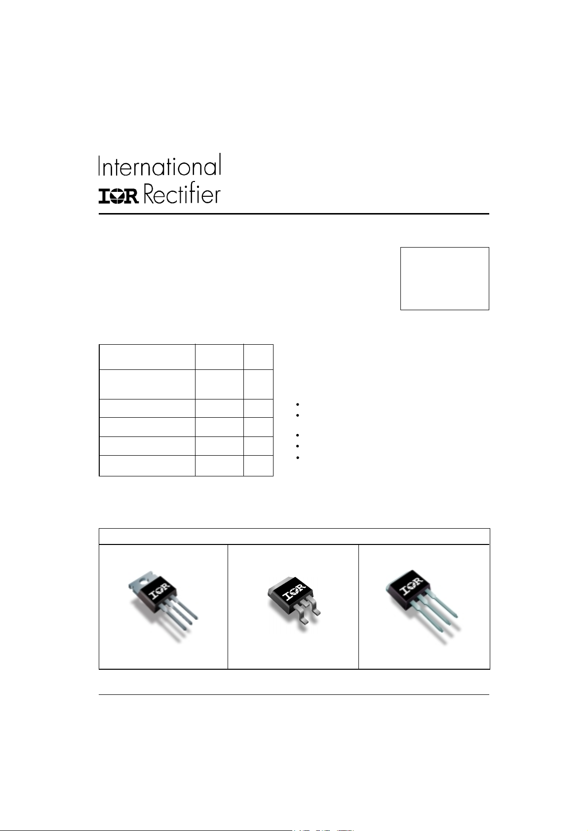
Case Styles
32CTQ030 32CTQ030S 32CTQ030-1
2
TO-220 D
PAK TO-262
1
32CTQ030, 32CTQ030S, 32CTQ030-1
Bulletin PD-20265 07/00
Voltage Ratings
Part number 32CTQ030
VRMax. DC Reverse Voltage (V)
V
Max. Working Peak Reverse Voltage (V)
RWM
30
Absolute Maximum Ratings
Parameters 32CTQ Units Conditions
I
Max. Average Forward Current 30 A 50% duty cycle @ TC = 115° C, rectangular wave form
F(AV)
* See Fig. 5
I
Max. Peak One Cycle Non-Repetitive 900 5µs Sine or 3µs Rect. pulse
FSM
Surge Current * See Fig. 7 250 10ms Sine or 6ms Rect. pulse
EASNon-Repetitive Avalanche Energy 13 mJ TJ = 25 °C, I
A
= 1.20 Amps, L = 11.10 mH
AS
IARRepetitive Avalanche Current 3 A Current decaying linearly to zero in 1 µsec
Frequency limited by T
J
Following any rated
load condition and
with rated V
RRM
max. VA = 1.5 x VR typical
applied
Electrical Specifications
Parameters 32CTQ Units Conditions
VFMMax. Forward Voltage Drop (1) 0.49 V @ 15A
* See Fig. 1 0.58 V @ 30A
0.40 V @ 15A
0.53 V @ 30A
IRMMax. Reverse Leakage Current (1) 1.75 mA TJ = 25 °C
* See Fig. 2 97 mA TJ = 125 °C
V
Threshold Voltage 0.233 V T
F(TO)
r
Forward Slope Resistance 9.09 mΩ
t
= TJ max.
J
CTMax. Junction Capacitance Per Leg 1300 pF VR = 5VDC, (test signal range 100Khz to 1Mhz) 25 °C
LSTypical Series Inductance Per Leg 8.0 nH Measured lead to lead 5mm from package body
dv/dt Max. Voltage Rate of Change 10,000 V/ µs
(Rated V
)
R
TJ = 25 °C
TJ = 125 °C
VR = rated V
(1) Pulse Width < 300µs, Duty Cycle < 2%
R
Thermal-Mechanical Specifications
Parameters 32CTQ Units Conditions
TJMax. Junction Temperature Range - 55 to 150 °C
T
Max. Storage Temperature Range - 55 to 150 °C
stg
R
Max. Thermal Resistance Junction 3.25 °C/W DC operation * See Fig. 4
thJC
to Case Per Leg
R
Typical Thermal Resistance, 0.50 °C/W Mounting surface , smooth and greased
thCS
Case to Heatsink
wt Approximate Weight 2 (0.07) g (oz.)
T Mounting Torque Min. 6 (5)
Max. 12 (10)
Kg-cm
(Ibf-in)
2
www.irf.com

32CTQ030, 32CTQ030S, 32CTQ030-1
Bulletin PD-20265 07/00
1000
1000
100
T = 150 C
J
125 C
R
10
1
0.1
100
F
Reverse Current - I (m A)
0.01
0.001
100 C
75 C
50 C
25 C
0 5 10 15 20 25 30
Reverse Voltage - V (V)
R
Fig. 2 - Typical Values of Reverse Current
Vs. Reverse Voltage
10000
10
Instantaneous Forward Current - I (A)
T = 150 C
J
T = 125 C
J
T = 25 C
J
T
1000
T = 25 C
J
1
0 0.2 0.4 0.6 0.8 1 1.2 1.4 1.6 1.8
Forward Volta g e D rop - V (V)
Fig. 1 - Maximum Forward Voltage Drop Characteristics
10
D = 0.75
D = 0.50
D = 0.33
1
D = 0.25
thJC
Th ermal Im peda nce Z ( C/W )
D = 0.20
0.1
0.01
0.001
0.00001 0.0001 0.001 0.01 0.1 1 10
Sing le Pu lse
(Therm al Resistance)
t , Rectang ular P ulse D uration (Seco nds)
Fig. 4 - Maximum Thermal Impedance Z
www.irf.com
Junction Capacitance - C (pF)
100
0 5 10 15 20 25 30 35
FM
Reverse Voltage - V (V)
R
Fig. 3 - Typical Junction Capacitance
Vs. Reverse Voltage
P
DM
t
1
t
DM
2
1
thJC
2
C
Notes:
1. Duty factor D = t / t
2. Pea k T = P x Z + T
J
1
Characteristics
thJC
3

32CTQ030, 32CTQ030S, 32CTQ030-1
Bulletin PD-20265 07/00
160
150
140
130
120
Squa re wave (D = 0.50)
110
80% Rated V applied
R
100
90
Allowable Case Tem perature - ( C)
see n ote (2)
80
0 5 10 15 20 25
Averag e Forw ard Curren t - I (A)
Fig. 5 - Maximum Allowable Case Temperature
Vs. Average Forward Current
DC
F(AV)
1000
FSM
10
D = 0.20
D = 0.25
D = 0.33
8
D = 0.50
D = 0.75
RMS Limit
6
4
2
Average Power Loss - (Watts)
0
0 5 10 15 20 25
Average Forward Current - I (A)
Fig. 6 - Forward Power Loss Characteristics
DC
F(AV)
DUT
CURRENT
MONITOR
(2) Formula used: TC = TJ - (Pd + Pd
Pd = Forward Power Loss = I
Pd
= Inverse Power Loss = VR1 x IR (1 - D); IR @ V
REV
F(AV)
4
At Any Rated Load Condition
An d W ith Rated V Applied
Following Surge
Non-Repetitive Surge Current - I (A)
100
10 100 1000 10000
RRM
Square W ave Pulse D uration - t (m icrosec)
Fig. 7 - Maximum Non-Repetitive Surge Current
L
IRFP460
Rg = 25 ohm
FREE-WHEEL
DIO D E
40HFL40S02
Fig. 8 - Unclamped Inductive Test Circuit
) x R
REV
x VFM @ (I
;
thJC
/ D) (see Fig. 6);
F(AV)
= 80% rated V
R1
R
p
HIGH-SPEED
SWITCH
Vd = 25 Volt
+
www.irf.com

Outline Table
A
A
32CTQ030, 32CTQ030S, 32CTQ030-1
Bulletin PD-20265 07/00
15.24 (0.60)
14.84 (0.58)
14.09 (0.55)
13.47 (0.53)
4.57 (0.18)
4.32 (0.17)
BASE
COMMON
CATHODE
2
1.40 (0.05)
1.15 (0.04)
15.49 (0.61)
14.73 (0.58)
3X
10.54 (0.41)
MAX.
3
1
2
3
1
2
93°
1.40 (0.055)
1.14 (0.045)
3.78 (0.15)
3.54 (0.14)
2.92 (0.11)
2.54 (0.10)
TERM 2
3.96 (0.16)
3.55 (0.14)
2.04 (0.080) MAX.
0.94 (0.04)
0.69 (0.03)
5.08 (0.20) REF.
10.16 (0.40)
REF.
8.89 (0.35)
REF.
2X
DIA.
0.61 (0.02) MAX.
6.47 (0.25)
6.18 (0.24)
2.61 (0.10)
2.32 (0.09)
0.93 (0.37)
0.69 (0.27)
1.32 (0.05)
1.22 (0.05)
6.48 (0.25)
6.23 (0.24)
2°
0.10 (0.004)
BASE
2.89 (0.11)
2.64 (0.10)
COMMON
CATHODE
123
NODE
COMMON
CATHODE
12
Conform to JEDEC outline TO-220AB
Dimensions in millimeters and (inches)
4.69 (0.18)
4.20 (0.16)
1.32 (0.05)
1.22 (0.05)
5.28 (0.21)
4.78 (0.19)
0.55 (0.02)
0.46 (0.02)
MINIMUM RECOMMENDED FOOTPRINT
11.43 (0.45)
2
ANODE
123
COMMON
NODE
12
CATHODE
ANODE
13
2
Conform to JEDEC outline D2Pak (SMD-220)
Dimensions in millimeters and (inches)
www.irf.com
4.57 (0.18)
4.32 (0.17)
0.61 (0.02) M AX.
5.08 (0.20) REF.
8.89 (0.35)
3.81 (0.15)
2.08 (0.08)
2X
17.78 (0.70)
2.54 (0.10)
2X
5

32CTQ030, 32CTQ030S, 32CTQ030-1
A
Bulletin PD-20265 07/00
Outline Table
Modified JEDEC outline TO-262
Dimensions in millimeters and (inches)
BASE
COMMON
CATHODE
2
Ordering Information Table
Device Code
1 - Essential Part Number
2 - Common Cathode
3 - T = TO-220
4 - Q = Schottky Q Series
5 - Voltage Rating 030 = 30V
6 -S=D2Pak
6 - -1 = TO-262
6
32 C T Q 030 -1
1
3
524
123
COMMON
NODE
CATHODE
12
6
ANODE
www.irf.com
 Loading...