

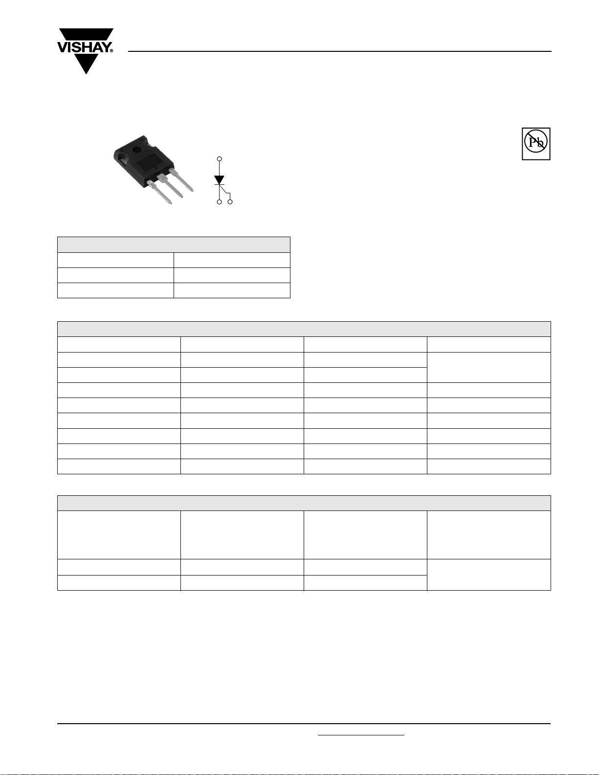
30TPS...PbF High Voltage Series
Vishay High Power Products
Phase Control SCR, 20 A
DESCRIPTION/FEATURES
TO-2 47 AC
PRODUCT SUMMARY
VT at 20 A < 1.3 V
I
TSM
V
RRM
2
(A)
1 (K)
(G) 3
300 A
800/1200 V
The 30TPS...PbF High Voltage Series of silicon
controlled rectifiers are specifically designed for
medium power switching and phase control
applications. The glass passivation technology
used has reliable operation up to 125 °C junction
temperature.
Typical applications are in input rectification (soft start) and
these products are designed to be used with Vishay HPP
input diodes, switches and output rectifiers which are
available in identical package outlines.
This product has been designed and qualified for industrial
level and lead (Pb)-free (“PbF” suffix).
MAJOR RATINGS AND CHARACTERISTICS
PARAMETER TEST CONDITIONS VALUES UNITS
I
T(AV)
I
RMS
V
RRM/VDRM
I
TSM
V
T
dV/dt 500 V/µs
dI/dt 150 A/µs
T
J
Sinusoidal waveform 20
30
800/1200 V
300 A
20 A, TJ = 25 °C 1.3 V
- 40 to 125 °C
A
Pb-free
Available
RoHS*
COMPLIANT
VOLTAGE RATINGS
V
RRM/VDRM
PART NUMBER
30TPS08PbF 800 900
30TPS12PbF 1200 1300
* Pb containing terminations are not RoHS compliant, exemptions may apply
Document Number: 94386 For technical questions, contact: diodes-tech@vishay.com
Revision: 06-Jun-08 1
REPETITIVE PEAK AND
OFF-STATE VOLTAGE
, MAXIMUM
V
V
, MAXIMUM
RSM
NON-REPETITIVE PEAK
REVERSE VOLTAGE
V
I
RRM/IDRM
AT 125 °C
mA
10
www.vishay.com
30TPS...PbF High Voltage Series
Vishay High Power Products
Phase Control SCR, 20 A
ABSOLUTE MAXIMUM RATINGS
PARAMETER SYMBOL TEST CONDITIONS VALUES UNITS
Maximum average on-state current I
Maximum RMS on-state current I
Maximum peak, one-cycle
non-repetitive surge current
2
Maximum I
Maximum I
t for fusing I2t
2
√t for fusing I2√t t = 0.1 to 10 ms, no voltage reapplied 4420 A2√s
Maximum on-state voltage drop V
On-state slope resistance r
Threshold voltage V
Maximum reverse and direct leakage current I
Maximum holding current I
Maximum latching current I
T(AV)
RMS
I
TSM
TM
t
T(TO)
RM/IDM
H
L
Maximum rate of rise of off-state voltage dV/dt 500 V/µs
Maximum rate of rise of turned-on current dI/dt 150 A/µs
TC = 95 °C, 180° conduction half sine wave 20
30
10 ms sine pulse, rated V
applied 250
RRM
10 ms sine pulse, no voltage reapplied 300
10 ms sine pulse, rated V
applied 310
RRM
10 ms sine pulse, no voltage reapplied 442
20 A, TJ = 25 °C 1.3 V
TJ = 125 °C
TJ = 25 °C
= 125 °C 10
T
J
V
= Rated V
R
RRM/VDRM
12 mΩ
1.0 V
0.5
Anode supply = 6 V, resistive load, initial IT = 1 A 100
Anode supply = 6 V, resistive load 200
A
A
mA
2
s
TRIGGERING
PARAMETER SYMBOL TEST CONDITIONS VALUES UNITS
Maximum peak gate power P
Maximum average gate power P
Maximum peak positive gate current + I
Maximum peak negative gate voltage - V
GM
G(AV)
GM
GM
8.0
2.0
1.5 A
10 V
W
Anode supply = 6 V, resistive load, TJ = - 10 °C 60
Maximum required DC gate current to trigger I
GT
Anode supply = 6 V, resistive load, T
= 25 °C 45
J
= 125 °C 20
J
mAAnode supply = 6 V, resistive load, T
Anode supply = 6 V, resistive load, TJ = - 10 °C 2.5
Maximum required DC gate
voltage to trigger
Maximum DC gate voltage not to trigger V
Maximum DC gate current not to trigger I
V
GT
GD
GD
Anode supply = 6 V, resistive load, T
Anode supply = 6 V, resistive load, T
TJ = 125 °C, V
= Rated value
DRM
= 25 °C 2.0
J
= 125 °C 1.0
J
V
0.25
2.0 mA
SWITCHING
PARAMETER SYMBOL TEST CONDITIONS VALUES UNITS
Typical turn-on time t
Typical turn-off time t
gt
rr
q
TJ = 25 °C 0.9
TJ = 125 °C
110
4
µsTypical reverse recovery time t
www.vishay.com For technical questions, contact: diodes-tech@vishay.com
Document Number: 94386
2 Revision: 06-Jun-08
30TPS...PbF High Voltage Series
Phase Control SCR, 20 A
Vishay High Power Products
THERMAL AND MECHANICAL SPECIFICATIONS
PARAMETER SYMBOL TEST CONDITIONS VALUES UNITS
Maximum junction and storage
temperature range
Maximum thermal resistance,
junction to case
Maximum thermal resistance,
junction to ambient
Maximum thermal resistance,
case to heatsink
Approximate weight
Mounting torque
Marking device Case style TO-247AC (JEDEC)
minimum 6 (5)
maximum 12 (10)
T
, T
J
Stg
R
thJC
DC operation
R
thJA
R
thCS
Mounting surface, smooth and greased 0.2
- 40 to 125 °C
0.8
40
6g
0.21 oz.
30TPS08
30TPS12
°C/W
kgf · cm
(lbf · in)
Document Number: 94386 For technical questions, contact: diodes-tech@vishay.com
Revision: 06-Jun-08 3
www.vishay.com

30TPS...PbF High Voltage Series
Vishay High Power Products
130
120
110
100
90
Maximum Allowable Case Temperature (°C)
0 5 10 15 20 25
Fig. 1 - Current Rating Characteristics
130
120
110
100
90
80
Maximum Allowable Case Temperature (°C)
0 5 10 15 20 25 30 35
Fig. 2 - Current Rating Characteristics
3 0 TPS. . Se r i e s
R (DC ) = 0.8 °C/ W
thJC
Conduction Angle
30°
60°
90°
120°
180°
Average On-state Current (A)
3 0 TPS. . Se ri e s
R ( DC) = 0.8 °C/ W
thJC
Conduction Period
30°
60°
90°
120°
180°
Average On-state Current (A)
Phase Control SCR, 20 A
DC
80
60
40
20
Maximum Avera g e On-sta t e Power Loss (W)
DC
180°
120°
90°
60°
30°
RM S Li m i t
Conduction Period
3 0TP S. . Se r ie s
T = 1 2 5 °C
J
0
0 1020304050
Average On-state Current (A)
Fig. 4 - On-State Power Loss Characteristics
280
At Any Rated Load Condition And With
Rat ed V Applied Follow ing Surge.
260
240
220
200
180
160
140
Peak Half Sine Wave On-state Current (A)
120
110100
Number Of Equal Amplitude Half Cycle Current Pulse s (N)
RRM
3 0 TPS. . Se r i e s
Init ial T = 125°C
J
@ 60 Hz 0.0083 s
@ 50 Hz 0.0100 s
Fig. 5 - Maximum Non-Repetitive Surge Current
60
50
40
30
20
10
0
Maximum Average On-sta te Power Loss (W)
0 5 10 15 20 25 30
180°
120°
90°
60°
30°
RM S Li m i t
Conduction Angle
30TPS.. Serie s
T = 125°C
J
Average On-state Current (A)
Fig. 3 - On-State Power Loss Characteristics
300
Maximum Non Re p et itive Surge Current
280
260
240
220
200
180
160
140
Peak Half Sine Wa ve On-sta t e C urren t (A)
120
Versus Pulse Train Duration. Control
Of Co nd uc t ion May Not Be Mainta ined.
30TPS.. Se rie s
0.01 0.1 1
Pulse Train Duration (s)
Initia l T = 125°C
No Vo lta ge Rea p plie d
Ra t e d V Re a p p l i e d
RRM
Fig. 6 - Maximum Non-Repetitive Surge Current
J
www.vishay.com For technical questions, contact: diodes-tech@vishay.com
Document Number: 94386
4 Revision: 06-Jun-08

30TPS...PbF High Voltage Series
Phase Control SCR, 20 A
1000
T = 2 5 °C
J
100
10
Instantaneous On-state Current (A)
1
01234567
Instantaneous On-state Voltage (V)
30TPS.. Serie s
T = 125°C
J
Vishay High Power Products
Fig. 7 - On-State Voltage Drop Characteristics
1
St e a d y St a t e V a l u e
(DC Operation)
0.1
D = 0.50
D = 0.33
D = 0.25
D = 0.17
D = 0.08
thJC
Si n g l e P u l se
30TPS.. Series
0.01
Transient Thermal Impedance Z (°C/ W)
0.0001 0.001 0.01 0.1 1
Square Wave Pulse Duration (s)
Fig. 8 - Thermal Impedance Z
100
Re c t a ng u la r g a te p u lse
a)Recommended load line for
rated di/dt: 10 V, 20 ohms
tr = 0.5 µs, tp >= 6 µs
b)Recommended load line for
<= 30% rated di/dt: 10 V, 65 ohms
10
tr = 1 µs, t p >= 6 µs
TJ = 2 5 ° C
TJ = 1 25 ° C
1
VGD
Instantaneous Gate Voltage (V)
0.1
IGD
0.001 0.01 0.1 1 10 100
30TPS.. Se rie s
Instantaneous Gate Current (A)
(a)
(b)
TJ = - 10 ° C
Characteristics
thJC
(1) PGM = 40 W, tp = 1 ms
(2) PGM = 20 W, tp = 2 ms
(3) PGM = 8 W, tp = 5 ms
(4) PGM = 4 W, t p = 10 ms
(3)
(4)
Frequency Limited by PG(AV)
Fig. 9 - Gate Characteristics
(2)
(1)
Document Number: 94386 For technical questions, contact: diodes-tech@vishay.com
www.vishay.com
Revision: 06-Jun-08 5

30TPS...PbF High Voltage Series
Vishay High Power Products
ORDERING INFORMATION TABLE
Device code
30 T P S 12 PbF
1 - Current rating (30 = 30 A)
2 - Circuit configuration:
3 - Package:
4
5 - Voltage code x 100 = V
6 -
Phase Control SCR, 20 A
51324
T = Thyristor
P = TO-247
- Type of silicon:
S = Standard recovery rectifier
RRM
None = Standard production
PbF = Lead (Pb)-free
6
08 = 800 V
12 = 1200 V
LINKS TO RELATED DOCUMENTS
Dimensions http://www.vishay.com/doc?95223
Part marking information http://www.vishay.com/doc?95226
www.vishay.com For technical questions, contact: diodes-tech@vishay.com
6 Revision: 06-Jun-08
Document Number: 94386

Legal Disclaimer Notice
Vishay
Notice
The products described herein were acquired by Vishay Intertechnology, Inc., as part of its acquisition of
International Rectifier’s Power Control Systems (PCS) business, which closed in April 2007. Specifications of the
products displayed herein are pending review by Vishay and are subject to the terms and conditions shown below.
Specifications of the products displayed herein are subject to change without notice. Vishay Intertechnology, Inc., or
anyone on its behalf, assumes no responsibility or liability for any errors or inaccuracies.
Information contained herein is intended to provide a product description only. No license, express or implied, by
estoppel or otherwise, to any intellectual property rights is granted by this document. Except as provided in Vishay's
terms and conditions of sale for such products, Vishay assumes no liability whatsoever, and disclaims any express
or implied warranty, relating to sale and/or use of Vishay products including liability or warranties relating to fitness
for a particular purpose, merchantability, or infringement of any patent, copyright, or other intellectual property right.
The products shown herein are not designed for use in medical, life-saving, or life-sustaining applications.
Customers using or selling these products for use in such applications do so at their own risk and agree to fully
indemnify Vishay for any damages resulting from such improper use or sale.
International Rectifier
are registered trademarks of International Rectifier Corporation in the U.S. and other countries. All other product
names noted herein may be trademarks of their respective owners.
®
, IR®, the IR logo, HEXFET®, HEXSense®, HEXDIP®, DOL®, INTERO®, and POWIRTRAIN
®
Document Number: 99901 www.vishay.com
Revision: 12-Mar-07 1
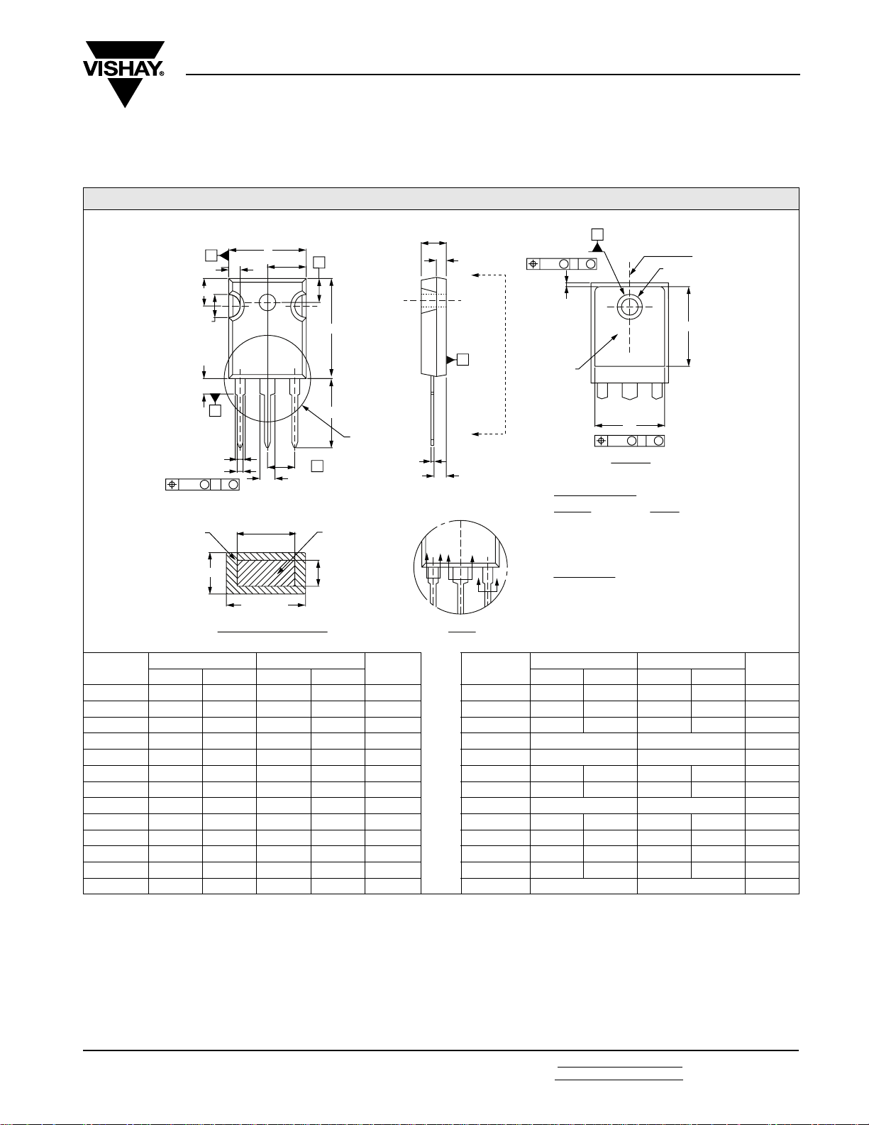
DIMENSIONS in millimeters and inches
Outline Dimensions
Vishay High Power Products
TO-247
(2) R/2
2 x R
(5) L1
0.10 AC
Planting
B
D
(2)
C
2 x b2
3 x b
MM
(c)
Section C - C, D - D, E - E
E
1
2
b4
(b1, b3, b5)
(b, b2, b4)
(3)
E/2
3
(4)
2 x e
S
D
L
Base metal
c1
See view B
A
A2
A
D
A
C
A1
DDE E
View B
A
(6)
Ø P
MM
Ø K BD
D2
Thermal pad
Lead assignments
HEXFET
1. - Gate
2. - Drain
3. - Source
4. - Drain
C
C
IGBTs, CoPAK
1. - Gate
2. - Collector
3. - Emitter
4. - Collector
4
(4)
E1
MM
0.01 BD
View A - A
(Datum B)
FP1
D1 (4)
Diodes
1. - Anode/open
2. - Cathode
3. - Anode
SYMBOL
MILLIMETERS INCHES
MIN. MAX. MIN. MAX. MIN. MAX. MIN. MAX.
NOTES SYMBOL
MILLIMETERS INCHES
NOTES
A 4.65 5.31 0.183 0.209 D2 0.51 1.30 0.020 0.051
A1 2.21 2.59 0.087 0.102 E 15.29 15.87 0.602 0.625 3
A2 1.50 2.49 0.059 0.098 E1 13.72 - 0.540 -
b 0.99 1.40 0.039 0.055 e 5.46 BSC 0.215 BSC
b1 0.99 1.35 0.039 0.053 FK 2.54 0.010
b2 1.65 2.39 0.065 0.094 L 14.20 16.10 0.559 0.634
b3 1.65 2.37 0.065 0.094 L1 3.71 4.29 0.146 0.169
b4 2.59 3.43 0.102 0.135 N 7.62 BSC 3
b5 2.59 3.38 0.102 0.133 FP 3.56 3.66 0.14 0.144
c 0.38 0.86 0.015 0.034 FP1 - 6.98 - 0.275
c1 0.38 0.76 0.015 0.030 Q 5.31 5.69 0.209 0.224
D 19.71 20.70 0.776 0.815 3 R 0.452 5.49 0.178 0.216
D1 13.08 - 0.515 - 4 S 5.51 BSC 0.217 BSC
Notes
(1)
Dimensioning and tolerancing per ASME Y14.5M-1994
(2)
Contour of slot optional
(3)
Dimension D and E do not include mold flash. Mold flash shall not exceed 0.127 mm (0.005") per side. These dimensions are measured at
the outermost extremes of the plastic body
(4)
Thermal pad contour optional with dimensions D1 and E1
(5)
Lead finish uncontrolled in L1
(6)
Ø P to have a maximum draft angle of 1.5 to the top of the part with a maximum hole diameter of 3.91 mm (0.154")
(7)
Outline conforms to JEDEC outline TO-247 with exception of dimension c
Document Number: 95223 For technical questions concerning discrete products, contact: diodes-tech@vishay.com
www.vishay.com
Revision: 11-Mar-08 For technical questions concerning module products, contact: ind-modules@vishay.com
1

Assembly
lot code
xxxxxxx
V P119X
A
Part Marking Information
Vishay High Power Products
TO-247
Example: This is a xxxxxxx with
Part number
C
Product version (optional):
P = Lead (Pb)-free
None = Standard
Date code:
Year 1 = 2001
Week 19
Line X
assembly lot code AC,
assembled on WW 19, 2001
in the assembly line ”X”
Document Number: 95226 For technical questions concerning discrete products, contact: diodes-tech@vishay.com
Revision: 28-Nov-08 For technical questions concerning module products, contact: ind-modules@vishay.com
www.vishay.com
1
 Loading...