

16TTS..PbF High Voltage Series
Vishay High Power Products
Phase Control SCR, 10 A
DESCRIPTION/FEATURES
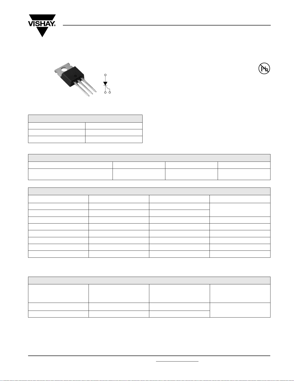
The 16TTS..PbF High Voltage Series of silicon
(A)
2
controlled rectifiers are specifically designed for
medium power switching and phase control
applications. The glass passivation technology
TO-220AB
(G) 3
used has reliable operation up to 125 °C junction
temperature.
1 (K)
Typical applications are in input rectification (soft start) and
PRODUCT SUMMARY
VT at 10 A < 1.4 V
I
TSM
V
RRM
200 A
800/1200 V
these products are designed to be used with Vishay HPP
input diodes, switches and output rectifiers which are
available in identical package outlines.
This product has been designed and qualified for industrial
level and lead (Pb)-free (“PbF” suffix).
OUTPUT CURRENT IN TYPICAL APPLICATIONS
APPLICATIONS SINGLE-PHASE BRIDGE THREE-PHASE BRIDGE UNITS
Capacitive input filter T
common heatsink of 1 °C/W
= 55 °C, TJ = 125 °C,
A
13.5 17 A
MAJOR RATINGS AND CHARACTERISTICS
PARAMETER TEST CONDITIONS VALUES UNITS
I
T(AV)
I
RMS
V
DRM/VRRM
I
TSM
V
T
dV/dt 500 V/µs
dI/dt 150 A/µs
T
J
Note
(1)
For higher voltage up to 1600 V contact factory
Sinusoidal waveform 10
16
(1)
Range
10 A, TJ = 25 °C 1.4 V
Range - 40 to 125 °C
800/1200 V
200 A
A
Available
RoHS*
COMPLIANT
VOLTAGE RATINGS
V
, MAXIMUM PEAK
PART NUMBER
16TTS08PbF 800 800
16TTS12PbF 1200 1200
* Pb containing terminations are not RoHS compliant, exemptions may apply
Document Number: 94603 For technical questions, contact: diodes-tech@vishay.com
Revision: 15-Sep-08 1
RRM
REVERSE VOLTAGE
V
V
, MAXIMUM PEAK
DRM
DIRECT VOLTAGE
V
I
RRM/IDRM
AT 125 °C
mA
10
www.vishay.com
16TTS..PbF High Voltage Series
Vishay High Power Products
Phase Control SCR, 10 A
ABSOLUTE MAXIMUM RATINGS
PARAMETER SYMBOL TEST CONDITIONS
Maximum average on-state current I
Maximum RMS on-state current I
Maximum peak, one-cycle,
non-repetitive surge current
2
Maximum I
Maximum I
t for fusing I2t
2
√t for fusing I2√t t = 0.1 to 10 ms, no voltage reapplied 2000 A2√s
Maximum on-state voltage drop V
On-state slope resistance r
Threshold voltage V
Maximum reverse and direct leakage current I
RM/IDM
Holding current I
Maximum latching current I
T(AV)
RMS
I
TSM
TM
t
T(TO)
H
L
TC = 98 °C, 180° conduction, half sine wave 10
16
10 ms sine pulse, rated V
applied 170
RRM
10 ms sine pulse, no voltage reapplied 200
10 ms sine pulse, rated V
applied 144
RRM
10 ms sine pulse, no voltage reapplied 200
10 A, TJ = 25 °C 1.4 V
TJ = 125 °C
TJ = 25 °C
T
= 125 °C 10
J
V
= Rated V
R
RRM/VDRM
Anode supply = 6 V, resistive load, initial IT = 1 A
16TTS08PbF, 16TTS12PbF
Anode supply = 6 V, resistive load 200
Maximum rate of rise of off-state voltage dV/dt 500 V/µs
Maximum rate of rise of turned-on current dI/dt 150 A/µs
VALUES
TYP. MAX.
24.0 mΩ
1.1 V
0.5
- 100
UNITS
A
2
A
s
mA
TRIGGERING
PARAMETER SYMBOL TEST CONDITIONS VALUES UNITS
Maximum peak gate power P
Maximum average gate power P
Maximum peak positive gate current + I
Maximum peak negative gate voltage - V
GM
G(AV)
GM
GM
8.0
2.0
1.5 A
10 V
W
Anode supply = 6 V, resistive load, TJ = - 65 °C 90
Maximum required DC gate current to trigger I
GT
Anode supply = 6 V, resistive load, T
Anode supply = 6 V, resistive load, T
= 25 °C 60
J
= 125 °C 35
J
mA
Anode supply = 6 V, resistive load, TJ = - 65 °C 3.0
Maximum required DC gate
voltage to trigger
Maximum DC gate voltage not to trigger V
Maximum DC gate current not to trigger I
V
GT
GD
GD
Anode supply = 6 V, resistive load, T
Anode supply = 6 V, resistive load, T
TJ = 125 °C, V
= Rated value
DRM
= 25 °C 2.0
J
= 125 °C 1.0
J
V
0.2
2.0 mA
SWITCHING
PARAMETER SYMBOL TEST CONDITIONS VALUES UNITS
Typical turn-on time t
Typical turn-off time t
gt
rr
q
TJ = 25 °C 0.9
TJ = 125 °C
4
110
µsTypical reverse recovery time t
www.vishay.com For technical questions, contact: diodes-tech@vishay.com
Document Number: 94603
2 Revision: 15-Sep-08
16TTS..PbF High Voltage Series
Phase Control SCR, 10 A
Vishay High Power Products
THERMAL AND MECHANICAL SPECIFICATIONS
PARAMETER SYMBOL TEST CONDITIONS VALUES UNITS
Maximum junction and storage
temperature range
Maximum thermal resistance,
junction to case
Maximum thermal resistance,
junction to ambient
Typical thermal resistance,
case to heatsink
Approximate weight
Mounting torque
Marking device Case style TO-220AB
minimum 6 (5)
maximum 12 (10)
T
, T
J
Stg
R
thJC
R
thJA
R
thCS
DC operation 1.3
Mounting surface, smooth and greased 0.5
- 40 to 125 °C
62
2g
0.07 oz.
16TTS08
16TTS12
°C/W
kgf · cm
(lbf · in)
Document Number: 94603 For technical questions, contact: diodes-tech@vishay.com
Revision: 15-Sep-08 3
www.vishay.com

16TTS..PbF High Voltage Series
Vishay High Power Products
125
120
115
110
105
100
95
90
024681012
Maximum Allowable Case Temperature (°C)
Fig. 1 - Current Rating Characteristics
125
120
115
110
16TTS.. Series
R (DC) = 1.3 °C/ W
thJC
Conduction Angle
30°
60°
90°
120°
Average On-state Current (A)
16TTS.. Serie s
R (DC) = 1.3 °C/ W
thJC
Conduction Period
Phase Control SCR, 10 A
180°
25
DC
180°
120°
20
90°
60°
30°
15
RM S Li m i t
10
Cond uction Period
5
0
Maximum Average On-state Power Loss (W)
0 2 4 6 8 1012141618
Average On-state Current (A)
16TTS.. Series
T = 12 5 ° C
J
Fig. 4 - On-State Power Loss Characteristics
180
At Any Rated Load Cond ition And With
Rated V App lied Following Surge.
RRM
160
140
Initial T = 125°C
J
@ 60 Hz 0.0083 s
@ 50 Hz 0.0100 s
105
100
95
90
0246810121416
Maximum Allowable Case Temperature (°C)
30°
60°
90°
120°
180°
Average On-state Current (A)
Fig. 2 - Current Rating Characteristics
18
180°
16
120°
90°
14
60°
30°
12
RM S Lim it
10
8
6
4
2
0
Maximum Average On-state Power Loss (W)
01234567891011
Average On-state Current (A)
Conduc tion Angle
16TTS.. Serie s
T = 12 5° C
J
Fig. 3 - On-State Power Loss Characteristics
DC
120
100
16TTS..Series
Peak Half Sine Wave On -stat e Current (A)
80
110100
Number Of Equal Amplitude Half Cycle Current Pulses (N)
Fig. 5 - Maximum Non-Repetitive Surge Current
200
Maximum Non Repetitive Surge Current
180
160
140
120
100
16TTS.. Series
Peak Half Sin e Wav e Forward Curren t (A )
80
0.01 0.1 1
Versus Pulse Train Dura tion .
Pulse Train Duration (s)
Initial T = 125°C
No Vo ltag e Reap plied
Ra t e d V Re a p p li e d
RRM
J
Fig. 6 - Maximum Non-Repetitive Surge Current
www.vishay.com For technical questions, contact: diodes-tech@vishay.com
Document Number: 94603
4 Revision: 15-Sep-08

16TTS..PbF High Voltage Series
Phase Control SCR, 10 A
1000
16TTS.. Serie s
100
10
T = 25 ° C
J
T = 125°C
J
Instantaneous On-state Current (A)
1
012345
Instantaneous On-state Voltage (V)
Vishay High Power Products
Fig. 7 - On-State Voltage Drop Characteristics
10
thJC
1
D = 0.50
D = 0.33
D = 0.25
D = 0.17
D = 0.08
0.1
Si n g le P ul se
Steady State Value
(DC Operation)
16TTS.. Series
0.01
Transient Thermal Impedance Z (°C/W)
0.0001 0.001 0.01 0.1 1 10
Squ a re Wave Pulse Dura tio n ( s)
Fig. 8 - Thermal Impedance Z
100
Rec tangular gate pulse
a)Recommended load line for
ra ted di /d t: 10 V, 20 o hms
tr = 0.5 µs, tp >= 6 µs
b)Recommended load line for
<= 30% rate d di/ dt : 10 V, 65 o hm s
10
tr = 1 µs, tp >= 6 µs
(b)
T
J = 25 °C
1
VGD
Instantaneous Gate Voltage (V)
0.1
IGD
0.001 0.01 0.1 1 10 100
TJ = 1 2 5 ° C
1 6TTS. . Se ri e s
Instantaneous Gate Current (A)
(a)
TJ = - 1 0 ° C
Characteristics
thJC
(1) PGM = 40 , tp = 1 ms
(2) PGM = 20 W, t p = 2 ms
(3) PGM = 8 W, t p = 5 ms
(4) PGM = 4 W, t p = 10 ms
(3)
(4)
Frequency Limited by PG(AV)
Fig. 9 - Gate Characteristics
(2)
(1)
Document Number: 94603 For technical questions, contact: diodes-tech@vishay.com
www.vishay.com
Revision: 15-Sep-08 5

16TTS..PbF High Voltage Series
Vishay High Power Products
ORDERING INFORMATION TABLE
Device code
16 T T S 12 PbF
1 - Current rating
2 - Circuit configuration:
3 - Package:
4
5
6
Phase Control SCR, 10 A
51324
T = Single thyristor
T = TO-220AB
- Type of silicon:
S = Converter grade
- Voltage code x 100 = V
-
None = Standard production
PbF = Lead (Pb)-free
RRM
6
08 = 800 V
12 = 1200 V
Note: For higher voltage up to 1600 V contact factory
LINKS TO RELATED DOCUMENTS
Dimensions http://www.vishay.com/doc?95222
Part marking information http://www.vishay.com/doc?95225
www.vishay.com For technical questions, contact: diodes-tech@vishay.com
6 Revision: 15-Sep-08
Document Number: 94603

Legal Disclaimer Notice
Vishay
Disclaimer
All product specifications and data are subject to change without notice.
Vishay Intertechnology, Inc., its affiliates, agents, and employees, and all persons acting on its or their behalf
(collectively, “Vishay”), disclaim any and all liability for any errors, inaccuracies or incompleteness contained herein
or in any other disclosure relating to any product.
Vishay disclaims any and all liability arising out of the use or application of any product described herein or of any
information provided herein to the maximum extent permitted by law. The product specifications do not expand or
otherwise modify Vishay’s terms and conditions of purchase, including but not limited to the warranty expressed
therein, which apply to these products.
No license, express or implied, by estoppel or otherwise, to any intellectual property rights is granted by this
document or by any conduct of Vishay.
The products shown herein are not designed for use in medical, life-saving, or life-sustaining applications unless
otherwise expressly indicated. Customers using or selling Vishay products not expressly indicated for use in such
applications do so entirely at their own risk and agree to fully indemnify Vishay for any damages arising or resulting
from such use or sale. Please contact authorized Vishay personnel to obtain written terms and conditions regarding
products designed for such applications.
Product names and markings noted herein may be trademarks of their respective owners.
Document Number: 91000 www.vishay.com
Revision: 18-Jul-08 1

DIMENSIONS in millimeters and inches
Outline Dimensions
Vishay High Power Products
TO-220AB
A
Ø P
E
Q
D
D1
3241
(3)
CC
e1
b, b2
c
b1, b3
Section C - C and D - D
Detail B
(2)
L1
DD
L
2 x e
MM
0.015 ABC
c1
C
H1
C
Lead assignments
HEXFET
1. - Gate
2. - Drain
3. - Source
IGBTs, CoPAK
1. - Gate
2. - Collector
3. - Emitter
B
A
Seating plane
A1
A2
Diodes
1. - Anode/open
2. - Cathode
3. - Anode
A
A
Sheet 2
3 x b2 3 x b
E
H1
θ
View A - A
123
C
C
Detail B
D
Thermal pad
D2
E1
D
L1
SYMBOL
MILLIMETERS INCHES
MIN. MAX. MIN. MAX. MIN. MAX. MIN. MAX.
NOTES SYMBOL
MILLIMETERS INCHES
NOTES
A 3.56 4.82 0.140 0.190 D1 8.38 9.02 0.330 0.355
A1 0.51 1.40 0.020 0.055 D2 12.19 12.88 0.480 0.507
A2 2.04 2.92 0.080 0.115 E 9.66 10.66 0.380 0.420 3
b 0.38 1.01 0.015 0.040 E1 8.38 8.89 0.330 0.350
b1 0.38 0.96 0.015 0.038 4 e 2.54 BSC 0.100 BSC
b2 1.15 1.77 0.045 0.070 H1 5.85 6.86 0.230 0.270
b3 1.15 1.73 0.045 0.068 L 12.70 14.73 0.500 0.580
c 0.36 0.61 0.014 0.024 L1 - 6.35 - 0.250 2
c1 0.36 0.56 0.014 0.022 4 Ø P 3.54 3.73 0.139 0.147
c2 0.31 1.14 0.012 0.045 Q 2.54 3.05 0.100 0.120
D 14.22 15.87 0.560 0.625 3 θ 90° to 93° 90° to 93°
Notes
(1)
Dimensioning and tolerancing per ASME Y14.5M-1994
(2)
Lead dimension and finish uncontrolled in L1
(3)
Dimension D and E do not include mold flash. Mold flash shall not exceed 0.127 mm (0.005") per side. These dimensions are measured at
the outermost extremes of the plastic body
(4)
Dimension b1 and c1 apply to base metal only
(5)
Controlling dimensions: inches
Document Number: 95222 For technical questions concerning discrete products, contact: diodes-tech@vishay.com
www.vishay.com
Revision: 11-Mar-08 For technical questions concerning module products, contact: ind-modules@vishay.com
1

Assembly
lot code
xxxxxxxx
V P119X
AC
TO-220AB
Part number
Product version (optional):
P = Lead (Pb)-free
None = Standard
Date code:
Year 1 = 2001
Week 19
Line X
Part Marking Information
Vishay High Power Products
Example: This is a xxxxxxxx with
assembly lot code AC,
assembled on WW 19, 2001
in the assembly line “X”
Document Number: 95225 For technical questions concerning discrete products, contact: diodes-tech@vishay.com
Revision: 30-Oct-08 For technical questions concerning module products, contact: ind-modules@vishay.com
www.vishay.com
1
 Loading...