

TO-208AA (TO-48)
Vishay High Power Products
Medium Power Thyristors
(Stud Version), 16 A
FEATURES
• Improved glass passivation for high reliability
and exceptional stability at high temperature
• High dI/dt and dV/dt capabilities
• Standard package
• Low thermal resistance
• Metric threads version available
• Types up to 1200 V V
• RoHS compliant
• Designed and qualified for industrial and consumer level
TYPICAL APPLICATIONS
16RIA Series
RoHS
COMPLIANT
DRM/VRRM
PRODUCT SUMMARY
I
T(AV)
16 A
• Medium power switching
• Phase control applications
• Can be supplied to meet stringent military, aerospace and
other high reliability requirements
MAJOR RATINGS AND CHARACTERISTICS
PARAMETER TEST CONDITIONS VALUES UNITS
I
T(AV)
I
T(RMS)
I
TSM
2
I
t
V
DRM/VRRM
t
q
T
J
T
C
50 Hz 340
60 Hz 360
50 Hz 574
60 Hz 524
Typical 110 µs
16 A
85 °C
35 A
A
A2s
100 to 1200 V
- 65 to 125 °C
Document Number: 93695 For technical questions, contact: ind-modules@vishay.com
Revision: 19-Sep-08 1
www.vishay.com
16RIA Series
Vishay High Power Products
Medium Power Thyristors
(Stud Version), 16 A
ELECTRICAL SPECIFICATIONS
VOLTAGE RATINGS
TYPE
NUMBER
VOLTAGE
CODE
V
DRM/VRRM
, MAXIMUM REPETITIVE PEAK
AND OFF-STATE VOLTAGE
V
(1)
10 100 150
20 200 300
40 400 500
16RIA
60 600 700
80 800 900
100 1000 1100
120 1200 1300
Notes
(1)
Units may be broken over non-repetitively in the off-state direction without damage, if dI/dt does not exceed 20 A/µs
(2)
For voltage pulses with tp ≤ 5 ms
ABSOLUTE MAXIMUM RATINGS
PARAMETER SYMBOL TEST CONDITIONS VALUES UNITS
Maximum average on-state current
at case temperature
Maximum RMS on-state current I
Maximum peak, one-cycle
non-repetitive surge current
2
Maximum I
Maximum I
t for fusing I2t
2
√t for fusing I2√t
Low level value of threshold voltage V
High level value of threshold voltage V
Low level value of
on-state slope resistance
High level value of
on-state slope resistance
Maximum on-state voltage V
Maximum holding current I
Latching current I
I
T(AV)
T(RMS)
180° sinusoidal conduction
35 A
t = 10 ms
I
TSM
t = 8.3 ms 360
t = 10 ms
t = 8.3 ms 300
t = 10 ms
t = 8.3 ms 524
t = 10 ms
t = 8.3 ms 375
t = 0.1 to 10 ms, no voltage reapplied,
= TJ maximum
T
J
T(TO)1
T(TO)2
r
t1
r
t2
TM
H
L
(16.7 % x π x I
T
= TJ maximum
J
(I > π x I
T(AV)
(16.7 % x π x I
T
= TJ maximum
J
(I > π x I
T(AV)
Ipk = 50 A, TJ = 25 °C 1.75 V
TJ = 25 °C, anode supply 6 V, resistive load
V
, MAXIMUM NON-REPETITIVE
RSM
PEAK VOLTAGE
(2)
AT T
V
16 A
85 °C
No voltage
340
reapplied
100 % V
RRM
reapplied
No voltage
reapplied
100 % V
RRM
Sinusoidal
half wave,
initial T
=
J
maximum
T
J
285
574
405
reapplied
5740 A
T(AV)
< I < π x I
T(AV)
),
0.97
), TJ = TJ maximum 1.24
T(AV)
< I < π x I
T(AV)
),
17.9
), TJ = TJ maximum 13.6
130
200
I
DRM/IRRM
= TJ MAXIMUM
J
mA
20
10
MAXIMUM
A
A
2
V
mΩ
mA
2
s
√s
www.vishay.com For technical questions, contact: ind-modules@vishay.com
Document Number: 93695
2 Revision: 19-Sep-08
16RIA Series
Medium Power Thyristors
Vishay High Power Products
(Stud Version), 16 A
SWITCHING
PARAMETER SYMBOL TEST CONDITIONS VALUES UNITS
≤ 600 V
V
DRM
≤ 800 V 180
V
Maximum rate of rise
of turned-on current
DRM
V
≤ 1000 V 160
DRM
V
≤ 1600 V 150
DRM
Typical turn-on time t
Typical reverse recovery time t
Typical turn-off time t
dI/dt
gt
rr
q
= TJ maximum, VDM = Rated V
T
J
DRM
Gate pulse = 20 V, 15 Ω, tp = 6 µs, tr = 0.1 µs maximum
I
= (2 x rated dI/dt) A
TM
TJ = 25 °C,
at rated V
DRM/VRRM
, TJ = 125 °C
TJ = TJ maximum,
= I
I
TM
TJ = TJ maximum, ITM = I
dI/dt = - 10 A/µs, dV/dt = 20 V/µs linear to 67 % V
, tp > 200 µs, dI/dt = - 10 A/µs
T(AV)
T(AV)
, tp > 200 µs, VR = 100 V,
DRM
gate bias 0 V to 100 W
Note
•t
= 10 µs up to 600 V, tq = 30 µs up to 1600 V available on special request
q
BLOCKING
PARAMETER SYMBOL TEST CONDITIONS VALUES UNITS
T
= TJ maximum linear to 100 % rated V
Maximum critical rate of rise
of off-state voltage
dV/dt
J
= TJ maximum linear to 67 % rated V
T
J
Note
(1)
Available with: dV/dt = 1000 V/µs, to complete code add S90 i.e. 16RIA120S90
DRM
DRM
200
0.9
4
,
110
100
(1)
300
A/µs
µs
V/µs
TRIGGERING
PARAMETER SYMBOL TEST CONDITIONS VALUES UNITS
Maximum peak gate power P
Maximum average gate power P
Maximum peak positive gate current I
Maximum peak negative gate voltage -V
DC gate current required to trigger I
DC gate voltage required to trigger V
DC gate current not to trigger I
DC gate voltage not to trigger V
GM
G(AV)
GM
GM
GT
GT
GD
GD
TJ = TJ maximum
TJ = TJ maximum 1.5 A
TJ = TJ maximum 10 V
TJ = - 65 °C
= 25 °C 60
J
= 125 °C 35
T
J
Maximum required gate trigger
current/voltage are the lowest
value which will trigger all units
6 V anode to cathode applied
TJ = - 65 °C 3.0
= 25 °C 2.0
T
J
= 125 °C 1.0
T
J
TJ = TJ maximum, V
= Rated value 2.0 mA
DRM
Maximum gate current/voltage
TJ = TJ maximum,
V
= Rated value
DRM
not to trigger is the maximum
value which will not trigger any
unit with rated V
anode to
DRM
cathode applied
8.0
2.0
90
mAT
0.2 V
W
V
Document Number: 93695 For technical questions, contact: ind-modules@vishay.com
www.vishay.com
Revision: 19-Sep-08 3

16RIA Series
Vishay High Power Products
Medium Power Thyristors
(Stud Version), 16 A
THERMAL AND MECHANICAL SPECIFICATIONS
PARAMETER SYMBOL TEST CONDITIONS VALUES UNITS
Maximum operating junction
and storage temperature range
Maximum thermal resistance,
junction to case
Maximum thermal resistance,
case to heatsink
Mounting torque
Approximate weight
Case style See dimensions - link at the end of datasheet TO-208AA (TO-48)
ΔR
CONDUCTION
thJC
CONDUCTION ANGLE SINUSOIDAL CONDUCTION RECTANGULAR CONDUCTION TEST CONDITIONS UNITS
180°
120°
90°
60°
30°
Note
• The table above shows the increment of thermal resistance R
T
, T
J
Stg
R
thJC
R
thCS
DC operation 0.86
Mounting surface, smooth, flat and greased 0.35
Lubricated threads
(Non-lubricated threads)
0.21 0.15
0.25 0.25
0.31 0.34
0.45 0.47
0.76 0.76
when devices operate at different conduction angles than DC
thJC
- 65 to 125 °C
TO NUT TO DEVICE
20 (27.5) 25 lbf ⋅ in
0.23 (0.32) 0.29 kgf · m
2.3 (3.1) 2.8 N · m
14 g
0.49 oz.
T
= TJ maximum K/W
J
K/W
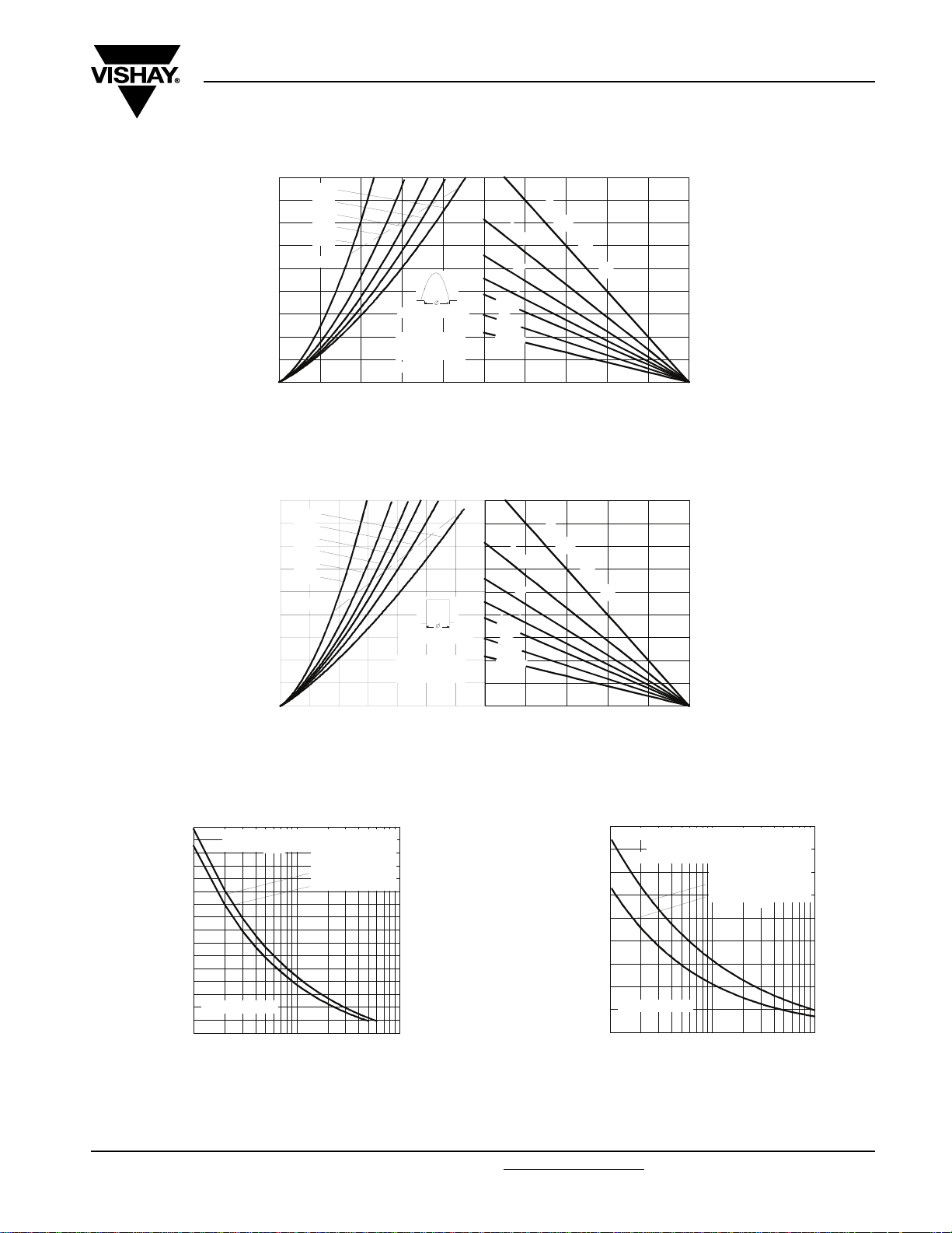
130
120
110
100
90
80
70
60
Maxi mu m Allo wabl e Case Temperature (°C)
50
0 5 10 15 20 25
16RIA Series
R (DC) = 1 .15 K/W
thJC
Conduction Angl e
30°
60°
90°
120°
Average On-state Current (A)
180°
130
120
110
100
90
80
70
60
Maximum All owable Case Temperature (°C)
50
010203040
16RIA Series
R (DC) = 1.15 K/W
thJC
Conduction Per iod
30°
60°
90°
120°
180°
Average On-state Current (A)
DC
Fig. 1 - Current Ratings Characteristics Fig. 2 - Current Ratings Characteristics
www.vishay.com For technical questions, contact: ind-modules@vishay.com
Document Number: 93695
4 Revision: 19-Sep-08
16RIA Series
Medium Power Thyristors
(Stud Version), 16 A
45
40
35
30
25
20
15
10
Maximum Average On-state Power Loss (W)
45
40
35
30
25
20
15
10
Maximum Average On-state Power Loss (W)
180°
120°
90°
60°
30°
RMS Limi t
Conducti on Angle
16RIA Series
T = 125°C
5
0
0 5 10 15 20 25
J
Average On-state Current (A)
Fig. 3 - On-State Power Loss Characteristics
DC
180°
120°
90°
60°
30°
RMS Limi t
Conducti on Period
16RIA Series
T = 125°C
5
0
0 4 8 1216202428
Average On-state Current (A)
J
Vishay High Power Products
R
t
h
S
A
2
K
3
K
/
W
4
K
/
W
5
K
/
W
7
K
/
W
1
0
K
/
W
0255075100125
Maximum Allowable Ambient Temperature (°C)
2
K
3
K
/
W
4
K
/
W
5
K
/
W
7K
/
W
1
0
K
/W
0255075100125
Maximu m All owa ble Ambi ent T emper atur e (°C)
=
0
/
W
/
W
.
1
K
/
W
D
e
l
t
a
R
R
t
h
S
A
=
0
.
1
K
/
W
D
e
l
t
a
R
Fig. 4 - On-State Power Loss Characteristics
300
280
260
At Any Rated Load Condition And With
Rated V Applied Following Surge.
RRM
Initial T = 125°C
J
@ 60 Hz 0.0083 s
@ 50 Hz 0.0100 s
240
220
200
180
16RIA Serie s
160
Peak Half Sine Wave On-state Current (A)
140
110100
Number Of Equal Amplitude Half Cycl e Curr ent Pulses (N)
Fig. 5 - Maximum Non-Repetitive Surge Current
350
Maxi mum Non Repeti ti ve Surge Cur ren t
325
300
275
Versus Pulse Train Durati on. Control
Of Conduction May Not Be Maintained.
Initial T = 125°C
No Voltage Reapplied
Rated V Reappli ed
J
RRM
250
225
200
175
16RIA Series
150
Peak Half Sine Wave On-state Current (A)
125
0.01 0.1 1
Pulse Train Duration (s)
Fig. 6 - Maximum Non-Repetitive Surge Current
Document Number: 93695 For technical questions, contact: ind-modules@vishay.com
www.vishay.com
Revision: 19-Sep-08 5

16RIA Series
Vishay High Power Products
1000
Instantaneous On-state Current (A)
10
Stead y State Val ue
R = 1.15 K/W
thJC
thJC
(DC Operation)
1
Medium Power Thyristors
(Stud Version), 16 A
16RIA Series
100
10
1
0.5 1 1.5 2 2.5 3 3.5
Instantaneous On-state Voltage (V)
Fig. 7 - Forward Voltage Drop Characteristics
T = 25°C
J
T = 125°C
J
0.1
16RIA Ser ies
Transient Thermal Impedance Z (K/W)
0.01
0.001 0.01 0.1 1 10
Square Wave Pulse Duration (s)
Fig. 8 - Thermal Impedance Z
100
Rectangular gate pulse
a) Recommended load line for
rated di/dt : 10V, 20ohms
tr <=0.5 µs, tp >= 6 µs
b) Recommended load li ne for
<=30% rated di/dt : 10V, 65ohms
10
tr<=1 µs, tp >= 6 µs
(b)
Tj = 25 °C
1
VGD
Instantaneous Gate Voltage (V)
0.1
IGD
0.001 0.0 1 0.1 1 10 100
Tj = 125 °C
Instantaneous Gate Current (A)
(a)
Tj = -65 °C
16RIA Series Frequency Limited by PG(AV)
Characteristics
thJC
(1) PGM = 16W, tp = 4ms
(2) PGM = 30W, tp = 2ms
(3) PGM = 60W, tp = 1ms
(4) PGM = 60W, tp = 1ms
(1)
Fig. 9 - Gate Characteristics
(4)
(3)
(2)
www.vishay.com For technical questions, contact: ind-modules@vishay.com
Document Number: 93695
6 Revision: 19-Sep-08

16RIA Series
Medium Power Thyristors
Vishay High Power Products
(Stud Version), 16 A
ORDERING INFORMATION TABLE
Device code
Dimensions http://www.vishay.com/doc?95333
16 RIA 120 M S90
51324
1 - Current code
- Essential part number
2
- Voltage code x 10 = V
3
- None = Stud base TO-208AA (TO-48) 1/4" 28UNF-2A
4
M = Stud base TO-208AA (TO-48) M6 x 1
- Critical dV/dt:
5
None = 300 V/µs (standard value)
S90 = 1000 V/µs (special selection)
LINKS TO RELATED DOCUMENTS
(see Voltage Ratings table)
RRM
Document Number: 93695 For technical questions, contact: ind-modules@vishay.com
Revision: 19-Sep-08 7
www.vishay.com

Legal Disclaimer Notice
Vishay
Disclaimer
All product specifications and data are subject to change without notice.
Vishay Intertechnology, Inc., its affiliates, agents, and employees, and all persons acting on its or their behalf
(collectively, “Vishay”), disclaim any and all liability for any errors, inaccuracies or incompleteness contained herein
or in any other disclosure relating to any product.
Vishay disclaims any and all liability arising out of the use or application of any product described herein or of any
information provided herein to the maximum extent permitted by law. The product specifications do not expand or
otherwise modify Vishay’s terms and conditions of purchase, including but not limited to the warranty expressed
therein, which apply to these products.
No license, express or implied, by estoppel or otherwise, to any intellectual property rights is granted by this
document or by any conduct of Vishay.
The products shown herein are not designed for use in medical, life-saving, or life-sustaining applications unless
otherwise expressly indicated. Customers using or selling Vishay products not expressly indicated for use in such
applications do so entirely at their own risk and agree to fully indemnify Vishay for any damages arising or resulting
from such use or sale. Please contact authorized Vishay personnel to obtain written terms and conditions regarding
products designed for such applications.
Product names and markings noted herein may be trademarks of their respective owners.
Document Number: 91000 www.vishay.com
Revision: 18-Jul-08 1

DIMENSIONS in millimeters (inches)
12.8 MAX.
(0.5 MAX.)
TO-208AA (TO-48)
Ø 1.7/1.8
(Ø 0.06/0.07)
30.2 MAX.
(0.18 MAX.)
22.2 MAX.
(0.87 MAX.)
Outline Dimensions
Vishay High Power Products
Ø 3.9/4.1
(Ø 0.15/0.16)
10.7/11.5
(0.42/0.45)
13.8/14.3
(0.54/0.56)
Across flats
1/4"-28UNF-2A
For metric device M6 x 1
Ø 15.5
(Ø 0.61)
45°
3.1/3.3
(0.12/0.13)
1.24/1.44
(0.04/0.05)
Document Number: 95333 For technical questions concerning discrete products, contact: diodes-tech@vishay.com
Revision: 07-Jul-08 For technical questions concerning module products, contact: ind-modules@vishay.com
www.vishay.com
1
 Loading...