

Bulletin PD-20192 rev. H 12/03
16CTQ...
16CTQ...S
16CTQ...-1
SCHOTTKY RECTIFIER
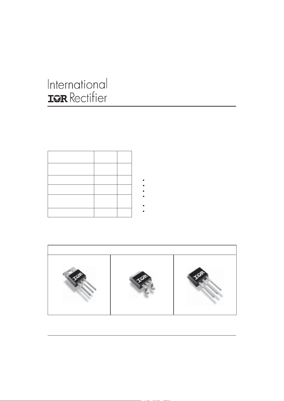
Major Ratings and Characteristics
Characteristics Values Units
I
Rectangular 16 A
F(AV)
waveform
V
RRM
I
@ tp = 5 µs sine 850 A
FSM
VF@ 8 Apk, TJ = 125°C 0.58 V
(per leg)
TJrange - 55 to 17 5 °C
60 / 100 V
16 Amp
Description/ Features
This center tap Schottky rectifier series has been optimized for
low reverse leakage at high temperature. The proprietary
barrier technology allows for reliable operation up to 175°C
junction temperature. Typical applications are in switching
power supplies, converters, free-wheeling diodes, and reverse
battery protection.
175° C TJ operation
Center tap configuration
Low forward voltage drop
High purity, high temperature epoxy encapsulation for
enhanced mechanical strength and moisture resistance
High frequency operation
Guard ring for enhanced ruggedness and long term
reliability
Case Styles
16CTQ... 16CTQ...S
TO-220 D
2
PAK TO-262
16CTQ...-1
1www.irf.com
16CTQ..., 16CTQ...S, 16CTQ...-1
Bulletin PD-20192 rev. H 12/03
Voltage Ratings
16CTQ060 16CTQ80 16CTQ100
Parameters
VRMax. DC Reverse Voltage (V)
V
Max. Working Peak Reverse Voltage (V)
RWM
16CTQ060S 16CTQ80S 16CTQ100S
16CTQ060-1 16CTQ80-1 16CTQ100-1
60 80 100
Absolute Maximum Ratings
Parameters Values Units Conditions
I
Max. Average Forward (Per Leg) 8 A 50% duty cycle @ TC = 148°C, rectangular wave form
F(AV)
Current * See Fig. 5 (Per Device) 16
I
Max. Peak One Cycle Non-Repetitive 850 5µs Sine or 3µs Rect. pulse
FSM
Surge Current (Per Leg) * See Fig. 7 275 10ms Sine or 6ms Rect. pulse
EASNon-Repetitive Avalanche Energy 7.50 mJ T
(Per Leg)
A
= 25 °C, I
J
= 0.50 Amps, L = 60 mH
AS
IARRepetitive Avalanche Current 0.50 A Current decaying linearly to zero in 1 µsec
(Per Leg) Frequency limited by TJ max. VA = 1.5 x VR typical
Following any rated
load condition and with
rated V
RRM
applied
Electrical Specifications
Parameters Values Units Conditions
VFMMax. Forward Voltage Drop 0.72 V @ 8A
(Per Leg) * See Fig. 1 (1) 0.88 V @ 16A
0.58 V @ 8A
0.69 V @ 16A
IRMMax. Reverse Leakage Current 0.55 mA TJ = 25 °C
(Per Leg) * See Fig. 2 (1) 7.0 mA TJ = 125 °C
V
Threshold Voltage 0.415 V T
F(TO)
= TJ max.
J
rtForward Slope Resistance 11.07 m Ω
CTMax. Junction Capacitance (Per Leg) 500 pF VR = 5VDC, (test signal range 100Khz to 1Mhz) 25°C
LSTypical Series Inductance (Per Leg) 8.0 nH Measured lead to lead 5mm from package body
dv/dt Max. Voltage Rate of Change 10,000 V/ µs
(Rated VR)
TJ = 25 °C
TJ = 125 °C
VR = rated V
(1) Pulse Width < 300µs, Duty Cycle <2%
R
Thermal-Mechanical Specifications
Parameters Values Units Conditions
TJMax. Junction Temperature Range -55 to 175 °C
T
Max. Storage Temperature Range -55 to 175 °C
stg
R
Max. Thermal Resistance Junction 3.25 °C/W DC operation
thJC
to Case (Per Leg)
R
Max. Thermal Resistance Junction 1.63 °C/W DC operation
thJC
to Case (Per Package)
R
Typical Thermal Resistance, Case 0.50 °C/W Mounting surface , smooth and greased
thCS
to Heatsink (only for TO-220)
wt Approximate Weight 2 (0.07) g (oz.)
T Mounting Torque Min. 6 (5)
Max. 12 (10)
Kg-cm
(Ibf-in)
2
www.irf.com
16CTQ..., 16CTQ...S, 16CTQ...-1
Bulletin PD-20192 rev. H 12/03
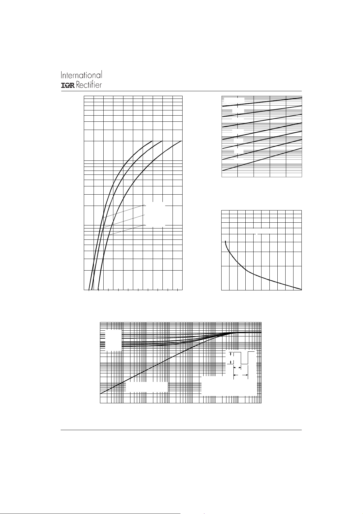
1000
100
F
T = 175°C
J
T = 125°C
J
10
Insta ntaneo us Forw a rd C urrent - I ( A)
T = 25°C
J
100
T = 175°C
J
10
150°C
R
125°C
1
100°C
Reve rse Current - I (mA)
0.0001
0.1
0.01
0.001
75°C
50°C
25°C
0 20406080100
Reve rse Vo lta ge - V (V)
R
Fig. 2 - Typical Values Of Reverse Current
Vs. Reverse Voltage (Per Leg)
1000
T
T = 25°C
J
1
0.2 0.4 0.6 0.8 1 1.2 1. 4 1.6 1.8 2 2.2
Fig. 1 - Max. Forward Voltage Drop Characteristics
Thermal Impedance Z (°C/W)
www.irf.com
Junction Capacitance - C (pF)
100
0 20406080100
Forward Voltage Drop - V (V)
FM
Reve rse Volta ge - V (V)
Fig. 3 - Typical Junction Capacitance
(Per Leg)
10
D = 0.7 5
D = 0.5 0
D = 0.3 3
1
D = 0.2 5
thJC
D = 0.20
0.1
0.01
0.001
0.00001 0.0001 0.001 0.01 0.1 1 10 100
Single Pulse
(Thermal Resistance)
t , Rectangular Pulse Duration (Seconds)
1
Fig. 4 - Max. Thermal Impedance Z
Note s:
1. Duty fa c tor D = t / t
2. Pe ak T = P x Z + T
Characteristics (Per Leg)
thJC
Vs. Reverse Voltage (Per Leg)
P
DM
t
1
t
2
J
1
DM
thJC
R
2
C
3

16CTQ..., 16CTQ...S, 16CTQ...-1
Bulletin PD-20192 rev. H 12/03
180
170
160
150
140
Sq u a r e w a v e ( D = 0 . 5 0 )
130
80% Rated V applied
R
120
110
Allowable Case Temperature - (°C)
see note (2)
100
02468101214
Average Forward Current - I (A)
Fig. 5 - Max. Allowable Case Temperature
Vs. Average Forward Current (Per Leg)
1000
FSM
DC
F( A V )
At Any Rated Load Condition
An d Wit h Rat e d V Ap p lied
Follow in g Surg e
RRM
7
D = 0.20
D = 0.25
6
D = 0.33
D = 0.50
5
D = 0.75
4
RM S Li m i t
DC
3
2
Average Power Loss - (Watts)
1
0
024681012
Average Forward Current - I (A)
Fig. 6 - Forward Power Loss Characteristics
(Per Leg)
F( A V )
DUT
C U RREN T
MONITOR
(2) Formula used: TC = TJ - (Pd + Pd
Pd = Forward Power Loss = I
Pd
= Inverse Power Loss = VR1 x IR (1 - D); IR @ V
REV
F(AV)
4
Non-Repetit ive Surge C urren t - I (A)
100
10 100 1 000 100 00
Square Wave Pulse Duration - t (microsec)
p
Fig. 7 - Max. Non-Repetitive Surge Current (Per Leg)
L
HI G H - SPEED
IRFP460
Rg = 25 ohm
SWITCH
FREE- W HEEL
DIODE
40HFL40S02
Fig. 8 - Unclamped Inductive Test Circuit
) x R
REV
x VFM @ (I
;
thJC
/ D) (see Fig. 6);
F(AV)
R1
= 10 V
Vd = 25 Volt
+
www.irf.com

A
Outline Table
A
16CTQ..., 16CTQ...S, 16CTQ...-1
Bulletin PD-20192 rev. H 12/03
15.24 (0.60)
14.84 (0.58)
14.09 (0.55)
13.47 (0.53)
1.40 (0.05)
1.15 (0.04)
4.57 (0.18)
4.32 (0.17)
BASE
COMMON
CATHODE
2
123
COMMON
NODE
12
CATHODE
ANODE
10.54 (0.41)
MAX.
1
2
1
2
15.49 (0.61)
14.73 (0.58)
1.40 (0.055)
3X
1.14 (0.045)
TERM 2
3
2.04 (0.080) MAX.
0.94 (0.04)
0.69 (0.03)
3
5.08 (0.20) REF.
93°
3.78 (0.15)
3.54 (0.14)
2.92 (0.11)
2.54 (0.10)
3.96 (0.16)
3.55 (0.14)
0.61 (0.02) MAX.
10.16 (0.40)
REF.
13
2
DIA.
2.61 (0.10)
2.32 (0.09)
8.89 (0.35)
REF .
0.93 (0.37)
2X
0.69 (0.27)
5.08 (0.20) REF.
6.48 (0.25)
6.23 (0.24)
6.47 (0.25)
6.18 (0.24)
4.57 (0.18)
4.32 (0.17)
0.61 (0.02) MAX.
1.32 (0.05)
1.22 (0.05)
2°
0.10 (0.004)
BASE
COMMON
CATHODE
2.89 (0.11)
2
2.64 (0.10)
123
COMMON
NODE
CATHODE
12
Conform to JEDEC outline TO-220AB
Dimensions in millimeters and (inches)
4.69 (0.18)
4.20 (0.16)
1.32 (0.05)
1.22 (0.05)
5.28 (0.21)
4.78 (0.19)
0.55 (0.02)
0.46 (0.02)
MINIMUM R ECOMME ND ED FOOTPR INT
11.43 (0.45)
8.89 (0.35)
3.81 (0.15)
17.78 (0.70)
ANODE
2.08 (0.08)
2X
Conform to JEDEC outline D2Pak (SMD-220)
2.54 (0.10)
2X
Dimensions in millimeters and (inches)
www.irf.com
5

16CTQ..., 16CTQ...S, 16CTQ...-1
A
Bulletin PD-20192 rev. H 12/03
Outline Table
Modified JEDEC outline TO-262
Dimensions in millimeters and (inches)
BASE
COMMON
CATHODE
2
123
COMMON
NODE
12
CATHODE
ANODE
Marking Information
THIS IS A 16CTQ100 S WITH
LOT CODE 58 07
ASSEMBLED ON WW 21, 2000
IN THE ASSEMBLY LINE "L"
6
INTERNATIONAL
RECTIFIER
LOGO
ASSEMBLY
LOT CODE
PART NUMBER
16CTQ100S
DATE CODE
YEAR 0 = 2000
WEEK 21
LINE L
www.irf.com
Tape & Reel Information
TRR
FEED DIRECTION
TRL
FEED DIRECTION
1.85 (0.073)
1.65 (0.065)
10.90 (0.429)
10.70 (0.421)
4.10 (0.161)
3.90 (0.153)
1.60 (0.063 )
1.50 (0.059 )
16CTQ..., 16CTQ...S, 16CTQ...-1
Bulletin PD-20192 rev. H 12/03
1.60 (0.063)
DIA.
1.50 (0.059)
11.60 (0.457)
11.40 (0.449)
1.75 (0.069)
1.25 (0.049)
16.10 (0.634)
15.90 (0.626)
DIA.
15.42 (0.609)
15.22 (0.601)
0.368 (0.0145)
0.342 (0.0135)
24.30 (0.957)
23.90 (0.941)
4.72 (0.18 6)
4.52 (0.17 8)
13.50 (0.532)
12.80 (0.504)
360 (1 4.173)
DIA. MAX.
Ordering Information Table
Device Code
1 - Essential Part Number
2 - C = Common Cathode
3 - T = TO-220
4 - Q = Schottky Q Series
5 - Voltage Rating
6 - 1 = TO-262
DIA.
26.40 (1.039)
24.40 (0.961)
16 C T Q 100 -1
1
S=D2Pak
3
524
SMD-220 Tape & Reel
When ordering, indicate the part
numb er, part orientat ion, and the
quantity. Qu antities are in m ultiples
of 800 p ieces per reel for both
60 (2 .362)
DIA. MIN.
TRL and T RR.
Dimensions in millimeters and (inches)
6
060 = 60V
080 = 80V
100 = 100V
www.irf.com
7

16CTQ..., 16CTQ...S, 16CTQ...-1
Bulletin PD-20192 rev. H 12/03
16CTQ100
********************************************
* SPICE Model Diode *
********************************************
.SUBCKT 16CTQ100 ANO CAT
D1 ANO 1 DMOD (0.07089)
*Define diode model
.MODEL DMOD D(IS=21.21E-06,N=1.578,Rs=7.804E-03,Ikf=0.9497, Xti=2, Eg=1.11
+ Cjo=1.278E-09, M=0.4736, Vj=0.4972, Fc=0.5, Irs=1.114e-21, Nr=4.755,
+ Bv=119.9, Ibv=215.5E-06, Tt=18.2E-09)
********************************************
.ENDS 16CTQ100
Thermal Model Subcircuit
.SUBCKT 16CTQ100 5 1
CTHERM1 5 4 1.45E+00
CTHERM2 4 3 4.54E+00
CTHERM3 3 2 1.09E+01
CTHERM4 2 1 1.01E+02
RTHERM1 5 4 2.49E+00
RTHERM2 4 3 5.20E-04
RTHERM1 3 2 5.43E-01
RTHERM1 2 1 3.05E-02
.ENDS 16CTQ100
Data and specifications subject to change without notice.
This product has been designed and qualified for Industrial Level.
Qualification Standards can be found on IR's Web site.
IR WORLD HEADQUARTERS: 233 Kansas St., El Segundo, California 90245, USA Tel: (310) 252-7105
TAC Fax: (310) 252-7309
Visit us at www.irf.com for sales contact information. 12/03
8
www.irf.com
 Loading...