

SMA
PRODUCT SUMMARY
I
F(AV)
V
R
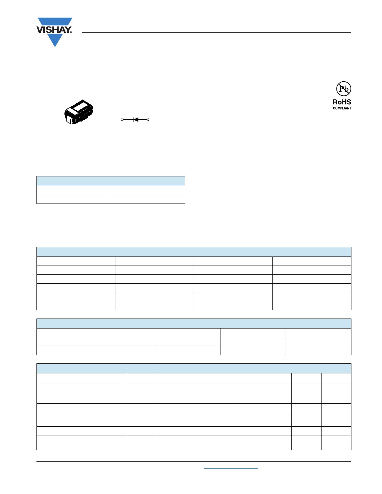
Schottky Rectifier, 3 A
Cathode Anode
3 A
40 V
VS-15MQ040NPbF
Vishay High Power Products
FEATURES
• Surface mountable
• Extremely low forward voltage
• Compact size
• Improved reverse blocking voltage capability
relative to other similar size Schottky
• Meets MSL level 1, per J-STD-020, LF maximum peak of
260 °C
• Compliant to RoHS directive 2002/95/EC
• Designed and qualified for industrial level
APPLICATIONS
• Switching power supplies
• Meter protection
• Reverse protection for power input to PC board circuits
• Battery isolation and charging
• Low threshold voltage diode
• Freewheeling or by-pass diode
• Low voltage clamp
DESCRIPTION
The VS-15MQ040NPbF Schottky rectifier is designed to be
used for low power applications where a reverse voltage of
40 V is encountered and surface mountable is required.
MAJOR RATINGS AND CHARACTERISTICS
SYMBOL CHARACTERISTICS VALUES UNITS
I
F(AV)
V
I
FSM
V
T
RRM
F
J
DC 3 A
40 V
tp = 5 μs sine 330 A
2 Apk, TJ = 125 °C 0.43 V
Range - 40 to 150 °C
VOLTAGE RATINGS
PARAMETER SYMBOL VS-15MQ040NPbF UNITS
Maximum DC reverse voltage V
Maximum working peak reverse voltage V
R
RWM
40 V
ABSOLUTE MAXIMUM RATINGS
PARAMETER SYMBOL TEST CONDITIONS VALUES UNITS
Maximum average forward current
See fig. 4
Maximum peak one cycle
non-repetitive surge current
See fig. 6
Non-repetitive avalanche energy E
Repetitive avalanche current I
I
F(AV)
I
FSM
AS
AR
50 % duty cycle at TL = 105 °C, rectangular waveform
On PC board 9 mm
(0.013 mm thick copper pad area)
5 μs sine or 3 μs rect. pulse
10 ms sine or 6 ms rect. pulse 140
TJ = 25 °C, IAS = 1 A, L = 12 mH 6.0 mJ
Current decaying linearly to zero in 1 μs
Frequency limited by T
2
island
Following any rated
load condition and with
rated V
RRM
maximum VA = 1.5 x VR typical
J
2.1 A
330
A
applied
1.0 A
Document Number: 94141 For technical questions, contact: diodestech@vishay.com
Revision: 04-Mar-10 1
www.vishay.com
VS-15MQ040NPbF
Vishay High Power Products
Schottky Rectifier, 3 A
ELECTRICAL SPECIFICATIONS
PARAMETER SYMBOL TEST CONDITIONS VALUES UNITS
1 A
Maximum forward voltage drop
See fig. 1
V
FM
2 A 0.49
(1)
1 A
2 A 0.43
Maximum reverse leakage current
See fig. 2
I
RM
Threshold voltage V
Forward slope resistance r
Typical junction capacitance C
Typical series inductance L
F(TO)
t
S
TJ = 25 °C
(1)
T
= 125 °C 20
J
TJ = TJ maximum
VR = 10 VDC, TJ = 25 °C, test signal = 1 MHz 134 pF
T
Measured lead to lead 5 mm from package body 2.0 nH
Maximum voltage rate of change dV/dt Rated V
T
= 25 °C
J
= 125 °C
T
J
V
= Rated V
R
R
R
0.42
0.34
0.5
0.26 V
64.6 mΩ
10 000 V/μs
Note
(1)
Pulse width < 300 μs, duty cycle < 2 %
THERMAL - MECHANICAL SPECIFICATIONS
PARAMETER SYMBOL TEST CONDITIONS VALUES UNITS
Maximum junction and storage
temperature range
Maximum thermal resistance,
junction to ambient
Approximate weight
Marking device Case style SMA (similar D-64) V3F
Note
dP
(1)
------------dT
1
tot
J
thermal runaway condition for a diode on its own heatsink
--------------<
R
thJA
(1)
T
, T
J
Stg
R
thJA
DC operation 80 °C/W
- 40 to 150 °C
0.07 g
0.002 oz.
V
mA
www.vishay.com For technical questions, contact: diodestech@vishay.com
Document Number: 94141
2 Revision: 04-Mar-10
VS-15MQ040NPbF
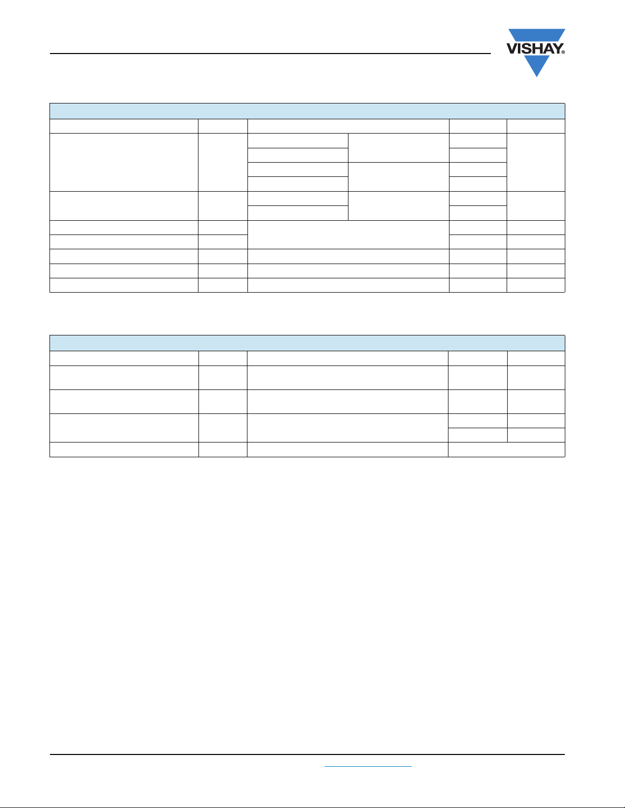
10
TJ = 150 °C
= 125 °C
T
1
J
= 25 °C
T
J
Current (A)
- Instantaneous Forward
F
I
0.1
0.2
0.3 0.5 0.7 0.9
V
- Forward Voltage Drop (V)
FM
0.80.60.4
Fig. 1 - Maximum Forward Voltage Drop Characteristics
100
TJ = 150 °C
10
1
0.1
- Reverse Current (mA)
0.01
R
I
0.001
TJ = 25 °C
01020
5
V
- Reverse Voltage (V)
R
TJ = 75 °C
TJ = 50 °C
TJ = 125 °C
TJ = 100 °C
30
352515
Fig. 2 - Typical Peak Reverse Current vs.
Reverse Voltage
Schottky Rectifier, 3 A
150
140
130
120
110
100
90
80
70
60
50
40
Allowable Case Temperature (°C)
30
1.6
1.4
1.2
1.0
0.8
0.6
0.4
Average Power Loss (W)
0.2
40
0
Fig. 5 - Maximum Average Forward Dissipation vs.
Vishay High Power Products
DC
D = 0.20
D = 0.25
D = 0.33
D = 0.50
D = 0.75
Square wave (D = 0.50)
See note (1)
0.5 1.5 2.5
0 2.0 3.01.0
I
F(AV)
80 % rated V
- Average Forward Current (A)
Fig. 4 - Maximum Average Forward Current vs.
Allowable Lead Temperature
D = 0.20
D = 0.25
D = 0.33
D = 0.50
D = 0.75
DC
0
I
- Average Forward Current (A)
F(AV)
1.51.00.5
Average Forward Current
applied
R
RMS limit
2.0 3.0
2.5
1000
100
- Junction Capacitance (pF)
T
C
10
5
020304045
15 25
10
V
- Reverse Voltage (V)
R
TJ = 25 °C
35
Fig. 3 - Typical Junction Capacitance vs. Reverse Voltage
1000
- Non-Repetitive Surge Current (A)
100
FSM
I
10
At any rated load condition
and with rated V applied
following surge
100
RRM
1000
10 000
tp - Square Wave Pulse Duration (µs)
Fig. 6 - Maximum Peak Surge Forward Current vs. Pulse Duration
Note
(1)
Formula used: TC = TJ - (Pd + Pd
Pd = Forward power loss = I
x VFM at (I
F(AV)
REV
) x R
;
thJC
/D) (see fig. 6); Pd
F(AV)
= Inverse power loss = VR1 x IR (1 - D); IR at VR1 = 80 % rated V
REV
R
Document Number: 94141 For technical questions, contact: diodestech@vishay.com
www.vishay.com
Revision: 04-Mar-10 3
VS-15MQ040NPbF
Vishay High Power Products
Schottky Rectifier, 3 A
ORDERING INFORMATION TABLE
Device code
Dimensions www.vishay.com/doc?95018
Part marking information www.vishay.com/doc?95029
Packaging information
SPICE model www.vishay.com/doc?95273
VS- 15 M Q 040 N TR PbF
51324678
1
- HPP product suffix
2 - Current rating
3 - M = SMA
4
- Q = Schottky “Q” series
5 - Voltage rating (040 = 40 V)
- N = New SMA
6
7 -
8
None = Box (1000 pieces)
TR = Tape and reel (7500 pieces)
- PbF = Lead (Pb)-free
LINKS TO RELATED DOCUMENTS
Tape and reel www.vishay.com/doc?95034
Bulk www.vishay.com/doc?95397
www.vishay.com For technical questions, contact: diodestech@vishay.com
4 Revision: 04-Mar-10
Document Number: 94141
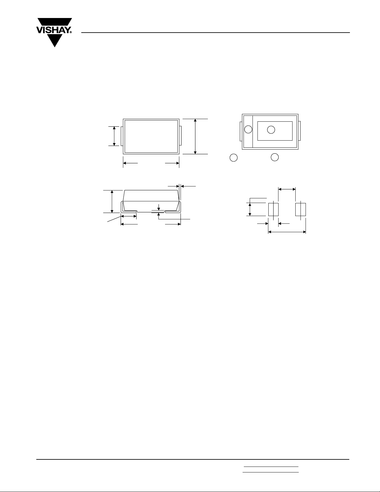
DIMENSIONS in millimeters (inches)
Outline Dimensions
Vishay High Power Products
SMA
1.40 (0.055)
1.60 (0.062)
2.00 (0.078)
2.44 (0.096)
0.76 (0.030)
1.52 (0.060)
4.00 (0.157)
4.60 (0.181)
4.80 (0.188)
5.28 (0.208)
2.50 (0.098)
2.90 (0.114)
0.152 (0.006)
0.305 (0.012)
0.103 (0.004)
0.203 (0.008)
12
Polarity Part Number
1
1.47 MIN.
(0.058 MIN.)
1.27 MIN.
(0.050 MIN.)
2
2.10 MAX.
(0.085 MAX. )
5.53 (0.218)
Soldering pad
Document Number: 95018 For technical questions concerning discrete products, contact: diodes-tech@vishay.com
Revision: 25-Jun-07 For technical questions concerning module products, contact: ind-modules@vishay.com
www.vishay.com
1

Legal Disclaimer Notice
www.vishay.com
Vishay
Disclaimer
ALL PRODUCT, PRODUCT SPECIFICATIONS AND DATA ARE SUBJECT TO CHANGE WITHOUT NOTICE TO IMPROVE
RELIABILITY, FUNCTION OR DESIGN OR OTHERWISE.
Vishay Intertechnology, Inc., its affiliates, agents, and employees, and all persons acting on its or their behalf (collectively,
“Vishay”), disclaim any and all liability for any errors, inaccuracies or incompleteness contained in any datasheet or in any other
disclosure relating to any product.
Vishay makes no warranty, representation or guarantee regarding the suitability of the products for any particular purpose or
the continuing production of any product. To the maximum extent permitted by applicable law, Vishay disclaims (i) any and all
liability arising out of the application or use of any product, (ii) any and all liability, including without limitation special,
consequential or incidental damages, and (iii) any and all implied warranties, including warranties of fitness for particular
purpose, non-infringement and merchantability.
Statements regarding the suitability of products for certain types of applications are based on Vishay’s knowledge of typical
requirements that are often placed on Vishay products in generic applications. Such statements are not binding statements
about the suitability of products for a particular application. It is the customer’s responsibility to validate that a particular
product with the properties described in the product specification is suitable for use in a particular application. Parameters
provided in datasheets and/or specifications may vary in different applications and performance may vary over time. All
operating parameters, including typical parameters, must be validated for each customer application by the customer’s
technical experts. Product specifications do not expand or otherwise modify Vishay’s terms and conditions of purchase,
including but not limited to the warranty expressed therein.
Except as expressly indicated in writing, Vishay products are not designed for use in medical, life-saving, or life-sustaining
applications or for any other application in which the failure of the Vishay product could result in personal injury or death.
Customers using or selling Vishay products not expressly indicated for use in such applications do so at their own risk. Please
contact authorized Vishay personnel to obtain written terms and conditions regarding products designed for such applications.
No license, express or implied, by estoppel or otherwise, to any intellectual property rights is granted by this document or by
any conduct of Vishay. Product names and markings noted herein may be trademarks of their respective owners.
Material Category Policy
Vishay Intertechnology, Inc. hereby certifies that all its products that are identified as RoHS-Compliant fulfill the
definitions and restrictions defined under Directive 2011/65/EU of The European Parliament and of the Council
of June 8, 2011 on the restriction of the use of certain hazardous substances in electrical and electronic equipment
(EEE) - recast, unless otherwise specified as non-compliant.
Please note that some Vishay documentation may still make reference to RoHS Directive 2002/95/EC. We confirm that
all the products identified as being compliant to Directive 2002/95/EC conform to Directive 2011/65/EU.
Vishay Intertechnology, Inc. hereby certifies that all its products that are identified as Halogen-Free follow Halogen-Free
requirements as per JEDEC JS709A standards. Please note that some Vishay documentation may still make reference
to the IEC 61249-2-21 definition. We confirm that all the products identified as being compliant to IEC 61249-2-21
conform to JEDEC JS709A standards.
Revision: 02-Oct-12
1
Document Number: 91000
 Loading...