

Ultrafast Rectifier
Bulletin PD-20031 rev. C 11/03
15ETH03
15ETH03S
15ETH03-1
Features
• Ultrafast Recovery Time
• Low Forward Voltage Drop
• Low Leakage Current
• 175°C Operating Junction Temperature
Description/ Applications
International Rectifier's 300V series are the state of the art Ultrafast recovery rectifiers designed with optimized
performance of forward voltage drop and Ultrafast recovery time.
The planar structure and the platinum doped life time control guarantee the best overall performance, ruggedness
and reliability characteristics.
These devices are intended for use in the output rectification stage of SMPS, UPS, DC-DC converters as well as
freewheeling diodes in low voltage inverters and chopper motor drives.
Their extremely optimized stored charge and low recovery current minimize the switching losses and reduce over
dissipation in the switching element and snubbers.
t
= 40ns
rr
I
= 15Amp
F(AV)
VR = 300V
Absolute Maximum Ratings
Parameters Max Units
V
RRM
I
F(AV)
I
FSM
TJ, T
Repetitive Peak Reverse Voltage 300 V
Average Rectified Forward Current @ TC = 142°C 15 A
Non Repetitive Peak Surge Current @ T J = 25°C 140
Operating Junction and Storage Temperatures - 65 to 175 °C
STG
www.irf.com
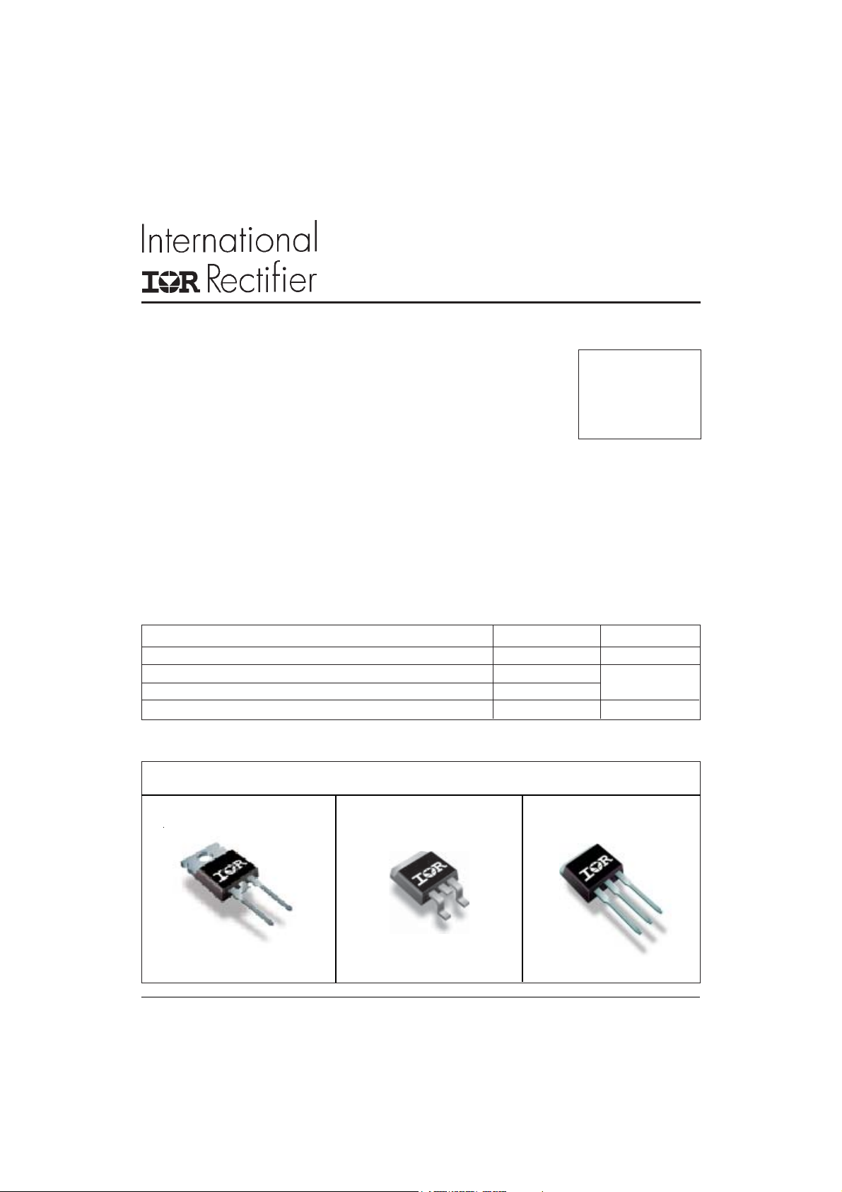
15ETH03
TO-220AC
Case Styles
15ETH03S
2
PAK
D
15ETH03-1
TO-262
1
15ETH03, 15ETH03S, 15ETH03-1
Bulletin PD-20031 rev. C 11/03
Electrical Characteristics @ T
= 25°C (unless otherwise specified)
J
Parameters Min Typ Max Units Test Conditions
VBR, VrBreakdown Voltage, 300 - - V I R = 100µA
Blocking Voltage
V
Forward Voltage - 1.05 1.25 V I F = 15A, TJ = 25°C
F
- 0.85 1.00 V I F = 15A, TJ = 125°C
I
R
Reverse Leakage Current - 0.05 40 µA V R = VR Rated
- 12 400 µA TJ = 125°C, VR = VR Rated
C
L
Junction Capacitance - 45 - pF V R = 300V
T
Series Inductance - 8 - nH .
S
Measured lead to lead 5mm from package body
Dynamic Recovery Characteristics @ TJ = 25°C (unless otherwise specified)
Parameters Min Typ Max Units Test Conditions
t
rr
I
RRM
Q
Reverse Recovery Time - - 40 ns IF = 1.0A, diF/dt = 50A/µs, VR = 30V
-32 - TJ = 25°C
45 - TJ = 125°C
Peak Recovery Current - 2.4 - A TJ = 25°C
- 6.1 - TJ = 125°C
Reverse Recovery Charge - 38 - nC TJ = 25°C
rr
- 137 - TJ = 125°C
I
= 15A
F
diF /dt = -200A/µs
VR = 200V
Thermal - Mechanical Characteristics
Parameters Min Typ Max Units
T
T
R
R
R
Wt Weight - 2.0 - g
Typical Socket Mount
Mounting Surface, Flat, Smooth and Greased
2
Max. Junction Temperature Range - 65 - 175 °C
J
Max. Storage Temperature Range - 65 - 175
Stg
Thermal Resistance, Junction to Case Per Leg - 1.02 2.0 °C/W
thJC
Thermal Resistance, Junction to Ambient Per Leg - - 70
thJA
Thermal Resistance, Case to Heatsink - 0.2 -
thCS
- 0.07 - (oz)
Mounting Torque 6.0 - 12 Kg-cm
5.0 - 10 lbf.in
www.irf.com
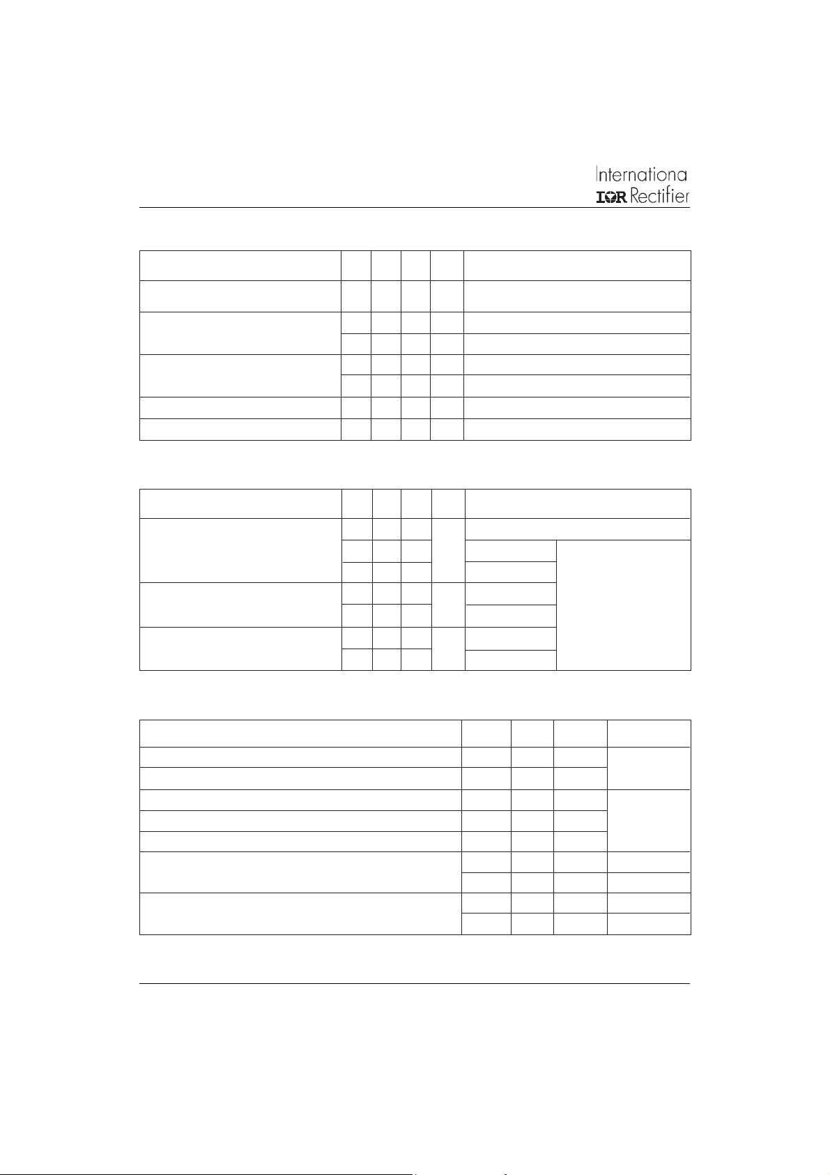
15ETH03, 15ETH03S, 15ETH03-1
0
Bulletin PD-20031 rev. C 11/03
100
(A)
F
10
Instantaneous Forward Current - I
Tj = 175˚C
Tj = 125˚C
Tj = 25˚C
1000
Tj = 175˚C
(µA)
R
100
10
1
150˚C
125˚C
100˚C
0.1
Reverse Current - I
0.01
0.001
0 50 100 150 200 250 300
Reverse Voltage - VR (V)
Fig. 2 - Typical Values Of Reverse Current
Vs. Reverse Voltage
1000
T = 25˚C
J
(pF)
T
100
25˚C
1
0.4 0.6 0.8 1 1.2 1.4 1.6
Forward Voltage Drop - VFM (V)
Fig. 1 - Typical Forward Voltage Drop Characteristics
10
(°C/W)
thJC
1
D = 0.50
D = 0.20
D = 0.10
D = 0.05
D = 0.02
0.1
D = 0.01
Thermal Impedance Z
Single Pulse
(Thermal Resistance)
0.01
0.00001 0.0001 0.001 0.01 0.1 1
t1, Rectangular Pulse Duration (Seconds)
Fig. 4 - Max. Thermal Impedance Z
www.irf.com
Junction Capacitance - C
10
0 50 100 150 200 250 30
Reverse Voltage - VR (V)
Fig. 3 - Typical Junction Capacitance
Vs. Reverse Voltage
P
DM
t
1
t
2
Notes:
1. Duty factor D = t1/ t2 .
2. Peak Tj = Pdm x ZthJC + Tc .
Characteristics
thJC
3
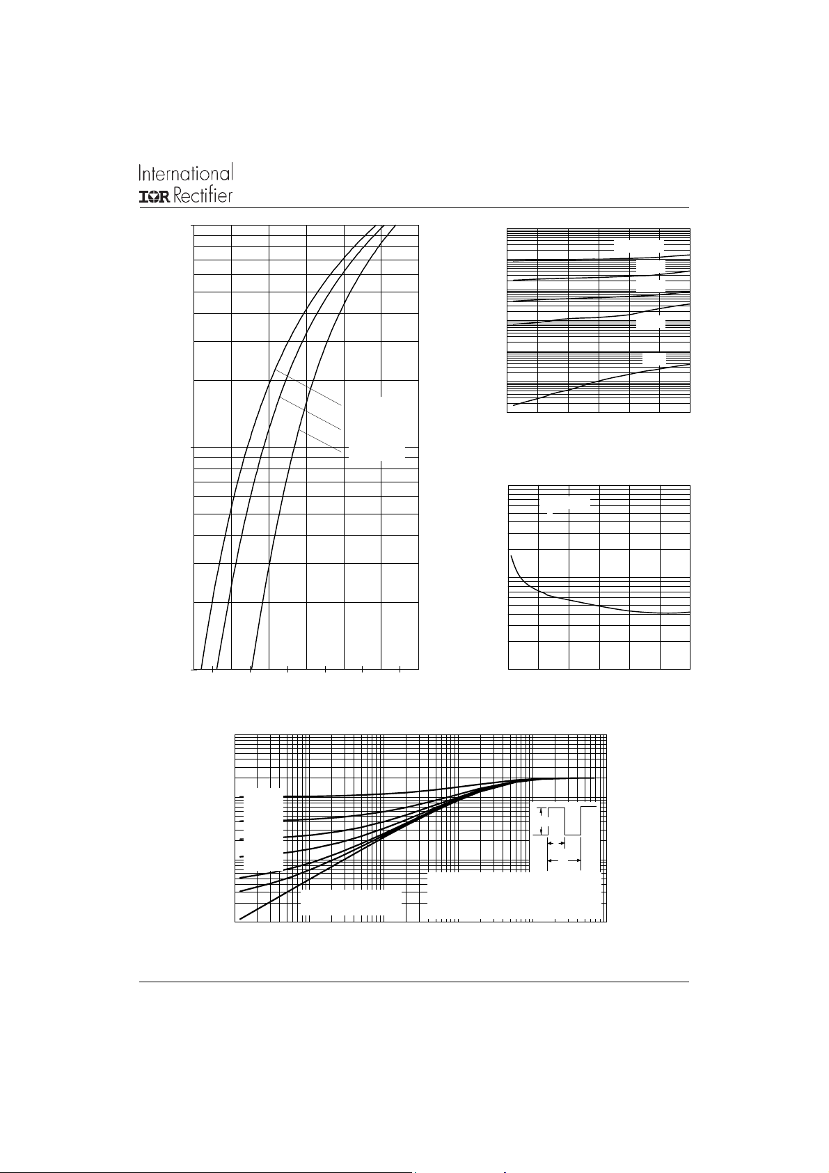
15ETH03, 15ETH03S, 15ETH03-1
Bulletin PD-20031 rev. C 11/03
180
170
160
150
140
Square wave (D = 0.50)
Rated Vr applied
130
see note (3)
Allowable Case Temperature (°C)
120
0 5 10 15 20 25
Average Forward Current - I
Fig. 5 - Max. Allowable Case Temperature
Vs. Average Forward Current
DC
F(AV)
(A)
22
20
18
16
RMS Limit
14
12
10
8
6
4
Average Power Loss ( Watts )
2
DC
D = 0.01
D = 0.02
D = 0.05
D = 0.10
D = 0.20
D = 0.50
0
0 5 10 15 20 25
Average Forward Current - I
Fig. 6 - Forward Power Loss Characteristics
F(AV)
(A)
100
trr ( ns )
10
100 1000
di
F
Fig. 7 - Typical Reverse Recovery vs. di
(3) Formula used: TC = TJ - (Pd + Pd
Pd = Forward Power Loss = I
Pd
= Inverse Power Loss = VR1 x IR (1 - D); IR @ V
REV
F(AV)
If = 15A, Tj = 25˚C
If = 15A, Tj = 125˚C
/dt (A/µs )
) x R
thJC
;
F(AV)
REV
x VFM @ (I
/dt
F
/ D) (see Fig. 6);
= rated V
R1
1000
If = 15A, Tj = 125˚C
100
Qrr ( nC )
10
100 1000
If = 15A, Tj = 25˚C
di F /dt (A/µs )
Fig. 8 - Typical Stored Charge vs. di
R
/dt
F
4
www.irf.com
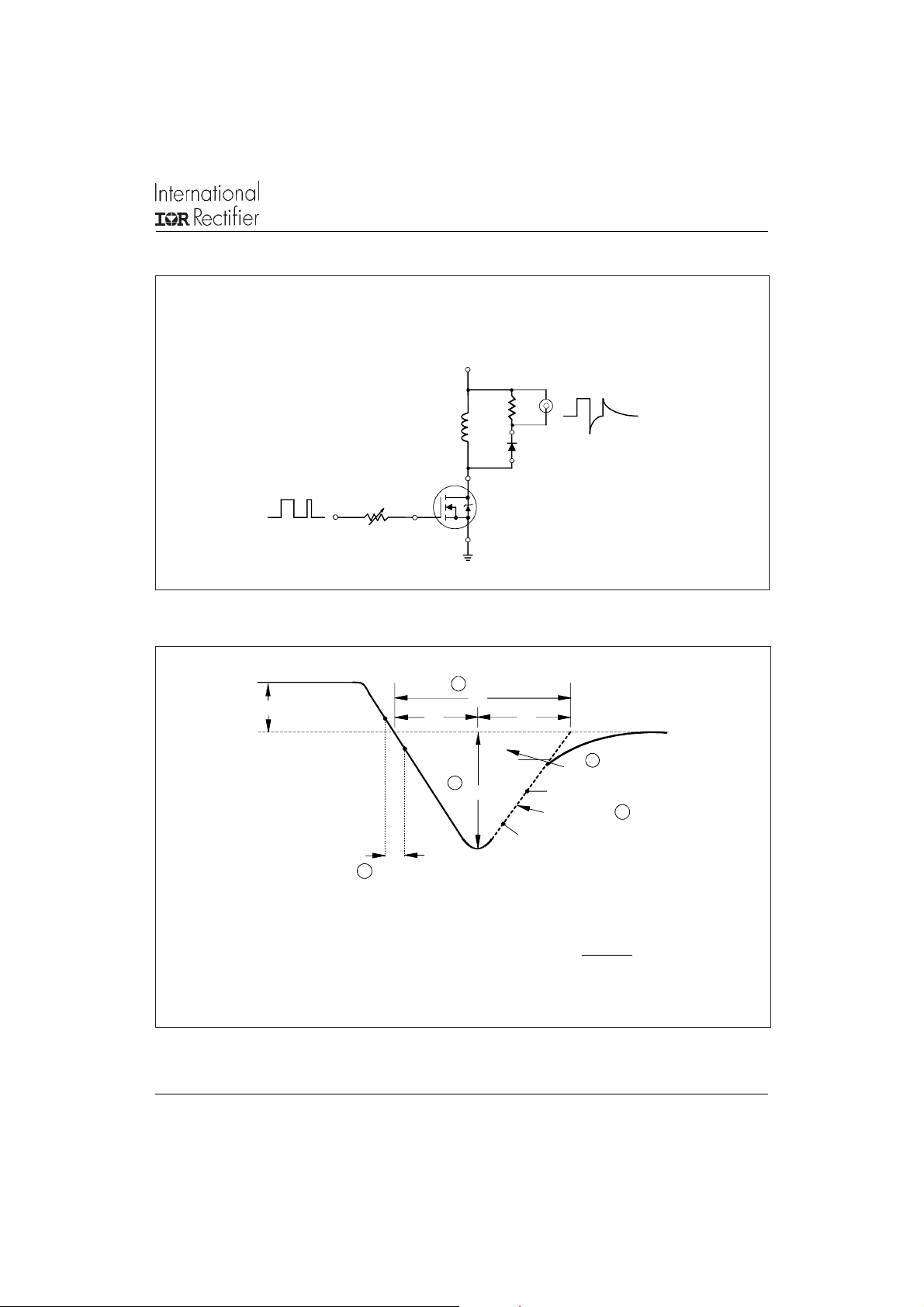
Reverse Recovery Circuit
V = 200V
R
Ω
0.01
L = 70µH
D.U.T.
15ETH03, 15ETH03S, 15ETH03-1
Bulletin PD-20031 rev. C 11/03
di F /dt
dif/dt
ADJUST
G
Fig. 9 - Reverse Recovery Parameter Test Circuit
I
F
t
a
0
1
di F /dt
di /dt
f
1. diF/dt - Rate of change of current through zero
crossing
2. I
- Peak reverse recovery current
RRM
3. t
- Reverse recovery time measured from zero
rr
crossing point of negative going IF to point where
a line passing through 0.75 I
extrapolated to zero current
RRM
and 0.50 I
RRM
3
2
D
IRFP250
S
t
rr
t
b
Q
I
RRM
0.5
di(rec)M/dt
0.75
I
RRM
4. Qrr - Area under curve defined by t
and I
RRM
Q
rr
5. di
/ dt - Peak rate of change of
(rec) M
current during t b portion of t
I
=
rr
RRM
t rr x I
4
5
rr
RRM
2
rr
www.irf.com
Fig. 10 - Reverse Recovery Waveform and Definitions
5

15ETH03, 15ETH03S, 15ETH03-1
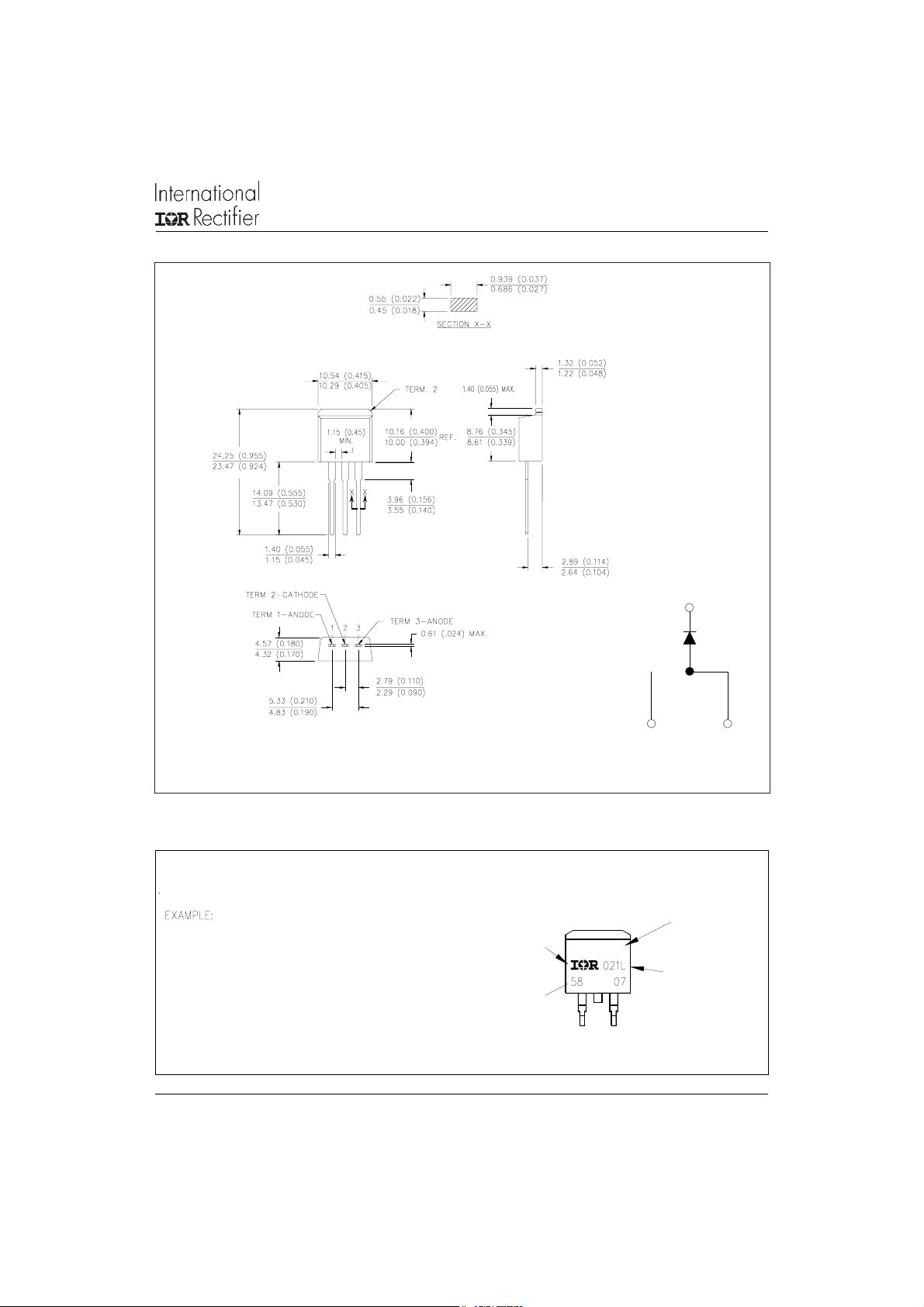
Anode
1
3
Base
Cathode
2
N/C
2
Anode
1
3
Cathode
Base
Cathode
Bulletin PD-20031 rev. C 11/03
Outline Table
15.24 (0.60)
14.84 (0.58)
14.09 (0.55)
13.47 (0.53)
4.57 (0.18)
4.32 (0.17)
15.49 (0.61)
14.73 (0.58)
3X
1.40 (0.05)
1.15 (0.04)
93°
1.40 (0.055)
1.14 (0.045)
10.54 (0.41)
MAX.
1
1
10.16 (0.40)
REF.
3
0.94 (0.04)
0.69 (0.03)
3
5.08 (0.20) REF.
2.61 (0.10)
2.32 (0.09)
8.89 (0.35)
REF.
0.93 (0.37)
2X
0.69 (0.27)
3.78 (0.15)
3.54 (0.14)
2.92 (0.11)
2.54 (0.10)
TERM 2
3.96 (0.16)
3.55 (0.14)
2.04 (0.080) MAX.
0.61 (0.02) MAX.
DIA.
6.48 (0.25)
6.23 (0.24)
1.32 (0.05)
1.22 (0.05)
2°
0.10 (0.004)
2.89 (0.11)
2.64 (0.10)
Conforms to JEDEC Outline TO-220AC
Dimensions in millimeters and (inches)
4.69 (0.18)
4.20 (0.16)
1.32 (0.05)
6.47 (0.25)
6.18 (0.24)
1.22 (0.05)
5.28 (0.21)
4.78 (0.19)
0.55 (0.02)
0.46 (0.02)
MINIMUM RECOMMENDED FOOTPRINT
11.43 (0.45)
13
2
4.57 (0.18)
4.32 (0.17)
0.61 (0.02) MAX.
5.08 (0.20) REF.
8.89 (0.35)
3.81 (0.15)
2.08 (0.08)
2X
17.78 (0.70)
2.54 (0.10)
2X
Conforms to JEDEC Outline D2PAK
Dimensions in millimeters and (inches)
6
www.irf.com
Outline Table
e
15ETH03, 15ETH03S, 15ETH03-1
Bulletin PD-20031 rev. C 11/03
2
Marking Information
THIS IS A 15ETH03S WITH
LOT CODE 58 07
ASSEMBLED ON WW 21, 2000
IN THE ASSEMBLY LINE "L"
www.irf.com
Conforms to JEDEC Outline TO-262
Dimensions in millimeters and (inches)
INTERNATIONAL
RECTIFIER
LOGO
ASSEMBLY
LOT CODE
15ETH03S
1
N/C
3
Anod
PART NUMBER
DATE CODE
YEAR 0 = 2000
WEEK 21
LINE L
7

15ETH03, 15ETH03S, 15ETH03-1
Bulletin PD-20031 rev. C 11/03
Part Marking Information
EXAMPLE: THIS IS A 15ETH03
LOT CODE 1789
ASSEMBLED ON WW 19, 1997
IN THE ASSEMBLY LINE "C"
TO-220AC
THIS IS A 15ETH03S WITH
LOT CODE 58 07
ASSEMBLED ON WW 21, 2000
IN THE ASSEMBLY LINE "L"
D2Pak
EXAMPLE: THIS IS A 15ETH03-1
LOT CODE 1789
ASSEMBLED ON WW 19, 1997
IN THE ASSEMBLY LINE "C"
INTERNATIONAL
RECTIFIER
LOGO
ASSEMBLY
LOT CODE
INTERNATIONAL
RECTIFIER
LOGO
ASSEMBLY
LOT CODE
INTERNATIONAL
RECTIFIER
LOGO
ASSEMBLY
LOT CODE
PART NUMBER
DATE CODE
YEAR 7 = 1997
WEEK 19
LINE C
PART NUMBER
DATE CODE
YEAR 0 = 2000
WEEK 21
LINE L
PART NUMBER
DATE CODE
YEAR 7 = 1997
WEEK 19
LINE C
TO-262
Data and specifications subject to change without notice.
This product has been designed and qualified for Industrial Level.
Qualification Standards can be found on IR's Web site.
IR WORLD HEADQUARTERS: 233 Kansas St., El Segundo, California 90245, USA Tel: (310) 252-7105
TAC Fax: (310) 252-7309
Visit us at www.irf.com for sales contact information. 11/03
8
www.irf.com
 Loading...