Vishay 12TTS08PbF Data Sheet

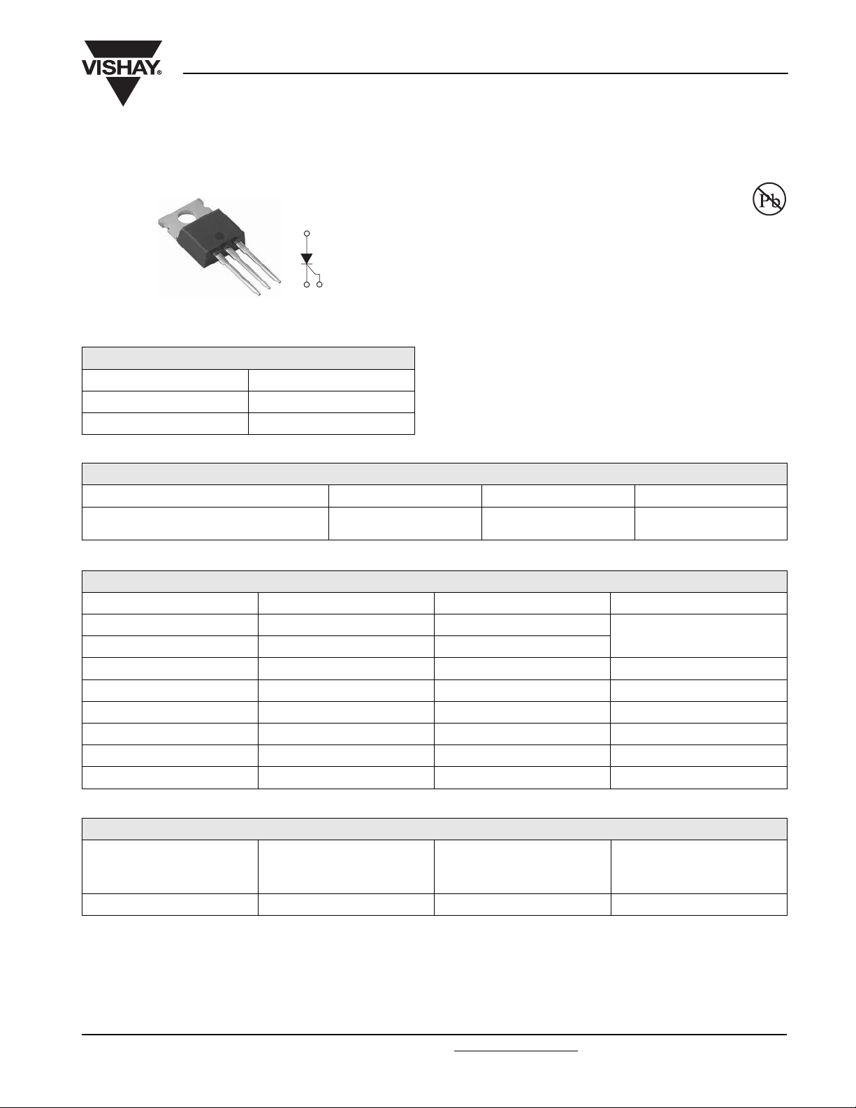
TO-220AB
PRODUCT SUMMARY
VT at 8 A 1.2 V
I
TSM
V
RRM
12TTS08PbF High Voltage Series
Vishay High Power Products
Phase Control SCR, 12.5 A
DESCRIPTION/FEATURES
(A)
1 (K)
2
(G) 3
140 A
800 V
The 12TTS08PbF High Voltage Series of silicon
controlled rectifiers are specifically designed for
medium power switching and phase control
applications. The glass passivation technology
used has reliable operation up to 125 °C junction
temperature.
Typical applications are in input rectification and crowbar
(soft start) and these products are designed to be used with
Vishay HPP input diodes, switches and output rectifiers
which are available in identical package outlines.
This product has been designed and qualified for industrial
level and lead (Pb)-free.
Available
RoHS*
COMPLIANT
OUTPUT CURRENT IN TYPICAL APPLICATIONS
APPLICATIONS SINGLE-PHASE BRIDGE THREE-PHASE BRIDGE UNITS
Capacitive input filter T
common heatsink of 1 °C/W
= 55 °C, TJ = 125 °C,
A
13.5 17 A
MAJOR RATINGS AND CHARACTERISTICS
PARAMETER TEST CONDITIONS VALUES UNITS
I
T(AV)
I
T(RMS)
V
DRM/VRRM
I
TSM
V
T
dV/dt 150 V/µs
dI/dt 100 A/µs
T
J
Sinusoidal waveform 8
12.5
800 V
140 A
8 A, TJ = 25 °C 1.2 V
Range - 40 to 125 °C
A
VOLTAGE RATINGS
V
, MAXIMUM
PART NUMBER
12TTS08PbF 800 800 1.0
RRM
PEAK VOLTAGE
V
V
, MAXIMUM PEAK
DRM
DIRECT VOLTAGE
V
I
RRM/IDRM
AT 125 °C
mA
* Pb containing terminations are not RoHS compliant, exemptions may apply
Document Number: 94380 For technical questions, contact: diodes-tech@vishay.com
Revision: 23-Apr-08 1
www.vishay.com

12TTS08PbF High Voltage Series
Vishay High Power Products
Phase Control SCR, 12.5 A
ABSOLUTE MAXIMUM RATINGS
PARAMETER SYMBOL TEST CONDITIONS VALUES UNITS
Maximum average on-state current I
Maximum RMS on-state current I
Maximum peak, one-cycle,
non-repetitive surge current
2
Maximum I
Maximum I
t for fusing I2t
2
√t for fusing I2√t t = 0.1 to 10 ms, no voltage reapplied, TJ = 125 °C 1000 A2√s
Maximum on-state voltage drop V
On-state slope resistance r
Threshold voltage V
Maximum reverse and direct leakage current I
Typical holding current I
Maximum latching current I
Maximum rate of rise of off-state voltage dV/dt T
T(AV)
T(RMS)
I
TSM
TM
t
T(TO)
RM/IDM
H
L
TC = 108 °C, 180° conduction, half sine wave
12.5
10 ms sine pulse, rated V
10 ms sine pulse, no voltage reapplied, T
10 ms sine pulse, rated V
10 ms sine pulse, no voltage reapplied, T
applied, TJ = 125 °C 120
RRM
= 125 °C 140
J
applied, TJ = 125 °C 72
RRM
= 125 °C 100
J
8 A, TJ = 25 °C 1.2 V
TJ = 125 °C
TJ = 25 °C
= 125 °C 1.0
T
J
V
= Rated V
R
RRM/VDRM
Anode supply = 6 V, resistive load, initial IT = 1 A 30
Anode supply = 6 V, resistive load 50
= 25 °C 150 V/µs
J
Maximum rate of rise of turned-on current dI/dt 100 A/µs
8
16.2 mΩ
0.87 V
0.05
A
A
mA
2
s
TRIGGERING
PARAMETER SYMBOL TEST CONDITIONS VALUES UNITS
Maximum peak gate power P
Maximum average gate power P
Maximum peak positive gate current + I
Maximum peak negative gate voltage - V
GM
G(AV)
GM
GM
8.0
2.0
1.5 A
10 V
W
Anode supply = 6 V, resistive load, TJ = - 65 °C 20
Maximum required DC gate current to trigger I
GT
Anode supply = 6 V, resistive load, T
Anode supply = 6 V, resistive load, T
= 25 °C 15
J
= 125 °C 10
J
mA
Anode supply = 6 V, resistive load, TJ = - 65 °C 1.2
Maximum required DC gate
voltage to trigger
Maximum DC gate voltage not to trigger V
Maximum DC gate current not to trigger I
V
GT
Anode supply = 6 V, resistive load, T
Anode supply = 6 V, resistive load, T
GD
GD
TJ = 125 °C, V
= Rated value
DRM
= 25 °C 1
J
= 125 °C 0.7
J
V
0.2
0.1 mA
SWITCHING
PARAMETER SYMBOL TEST CONDITIONS VALUES UNITS
Typical turn-on time t
Typical turn-off time t
gt
rr
q
TJ = 25 °C 0.8
TJ = 125 °C
100
3
µsTypical reverse recovery time t
www.vishay.com For technical questions, contact: diodes-tech@vishay.com
Document Number: 94380
2 Revision: 23-Apr-08

12TTS08PbF High Voltage Series
Phase Control SCR, 12.5 A
Vishay High Power Products
THERMAL AND MECHANICAL SPECIFICATIONS
PARAMETER SYMBOL TEST CONDITIONS VALUES UNITS
Maximum junction and storage
temperature range
Maximum thermal resistance,
junction to case
Maximum thermal resistance,
junction to ambient
Typical thermal resistance,
case to heatsink
Approximate weight
Mounting torque
Marking device Case style TO-220AB 12TTS08
minimum 6 (5)
maximum 12 (10)
T
, T
J
Stg
R
thJC
R
thJA
R
thCS
DC operation 1.5
Mounting surface, smooth and greased 0.5
- 40 to 125 °C
62
2g
0.07 oz.
°C/W
kgf · cm
(lbf · in)
Document Number: 94380 For technical questions, contact: diodes-tech@vishay.com
Revision: 23-Apr-08 3
www.vishay.com
 Loading...