

VIS VG3617161ET-8, VG3617161ET-7, VG3617161ET-6 Datasheet

VG3617161ET
1,048,576 x 16 - Bit
VIS
Description
The VG3617161ET is CMOS Synchronous Dynamic RAM organized as 524,288-word X 16-bit X 2-bank.
It is fabricated with an advanced submicron CMOS technology and designed to operate from a single 3.3V
power supply. This SDRAM is delicately designed with performance concern for current high-speed application. Programmable CAS Latency and Burst Length make it possible to be used in widely various domains. It
is packaged by using JEDEC standard pinouts and standard plastic 50-pin TSOP II.
Features
• Single 3.3V +/- 0.3V power supply
• Clock frequency:166MHz, 143MHz, 125MHz
• Fully synchronous with all signals referenced to a positive clock edge
• Programmable CAS Iatency (2,3)
• Programmable burst length (1,2,4,8,& Full page)
• Programmable wrap sequence (Sequential/Interleave)
• Automatic precharge and controlled precharge
• Auto refresh and self refresh modes
• Dual internal banks controlled by A11(Bank select)
• Simultaneous and independent two bank operation
• I/O level : LVTTL interface
• Random column access in every cycle
• X16 organization
• Byte control by LDQM and UDQM
• 4096 refresh cycles/64ms
• Burst termination by burst stop and precharge command
CMOS Synchronous Dynamic RAM
Document:1G5-0189 Rev.1 Page 1
VIS
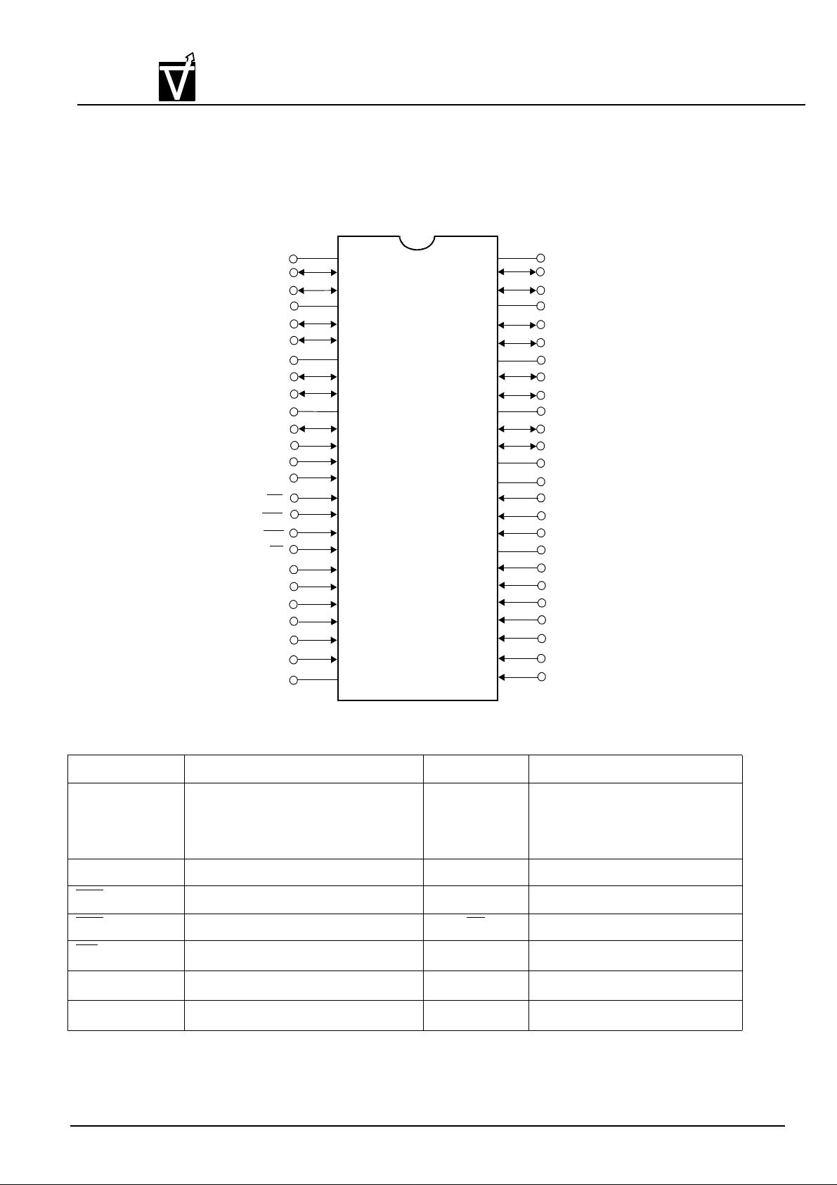
Pin Configuration
VG3617161ET
1,048,576 x 16 - Bit
CMOS Synchronous Dynamic RAM
50-Pin Plastic TSOP(II)(400 mil)
V
V
V
V
LDQM
CAS
(BS)A
V
DD
DQ0
DQ1
SSQ
DQ2
DQ3
DDQ
DQ4
DQ5
SSQ
DQ6
DQ7
DDQ
WE
RAS
CS
A
V
DD
1
2
3
4
5
6
7
8
9
10
11
12
13
14
15
16
17
18
11
10
A
0
A
1
A
2
A
3
19
20
21
22
23
24
25
VG3617161ET
50
49
48
47
46
45
44
43
42
41
40
39
38
37
36
35
34
33
32
31
30
29
28
27
26
V
SS
DQ15
DQ14
V
SSQ
DQ13
DQ12
V
DDQ
DQ11
DQ10
V
SSQ
DQ9
DQ8
V
DDQ
NC
UDQM
CLK
CKE
NC
A9
A8
A7
A6
A5
A4
V
SS
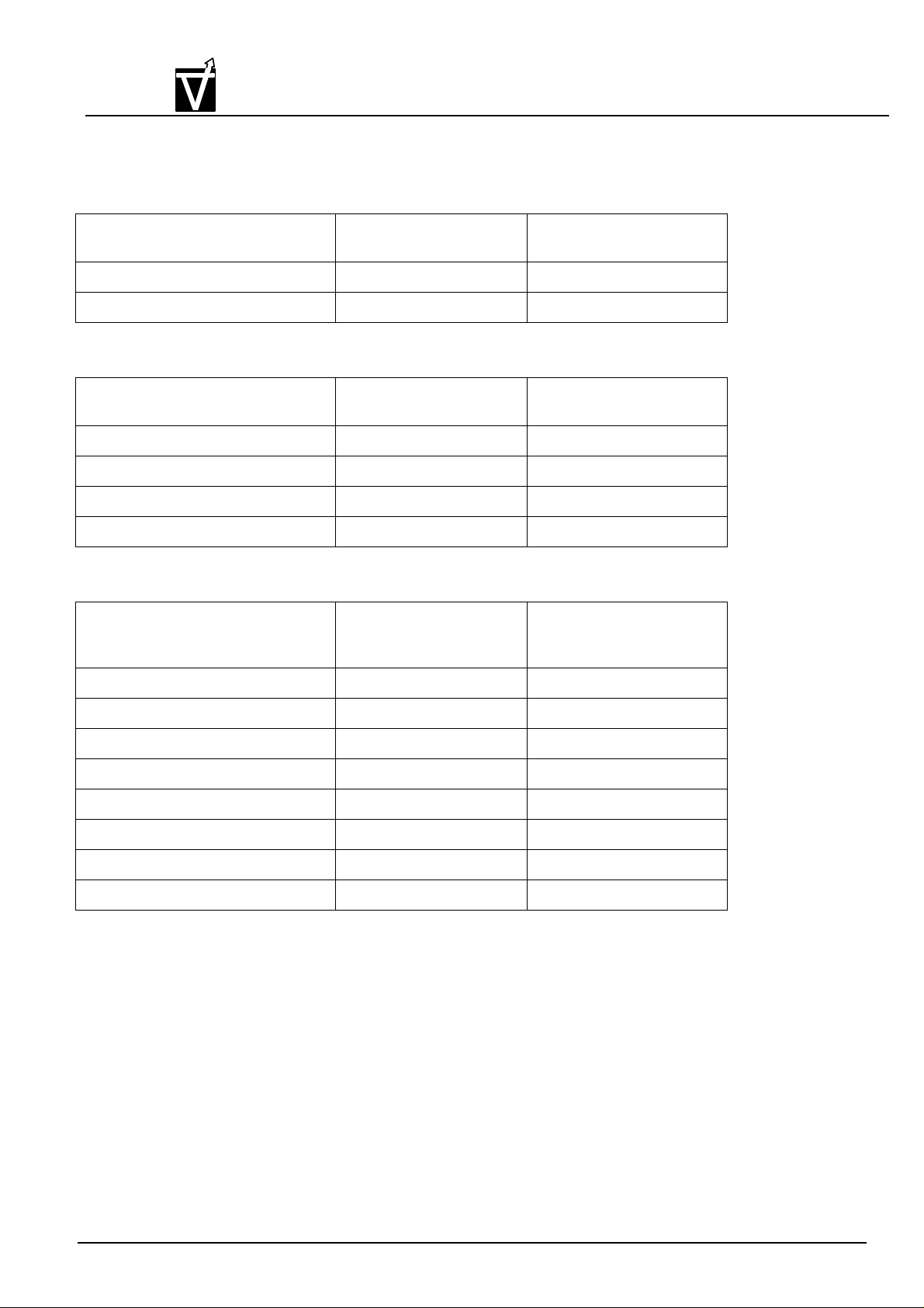
Pin Description
(VG3617161ET)
Pin Name Function Pin Name Function
A0-A11 Address inputs
- Row address A0-A10
LDQM,
UDQM
Lower DQ mask enable and
Upper DQ mask enable
- Column address A0-A7
A11: Bank select
DQ0~DQ15 Data-in/data-out CLK Clock input
RAS Row address strobe CKE Clock enable
CAS Column address strobe CS Chip select
WE Write enable V
V
SS
V
DD
Ground V
Power
DDQ
SSQ
Supply voltage for DQ
Ground for DQ
Document:1G5-0189 Rev.1 Page 2
VIS
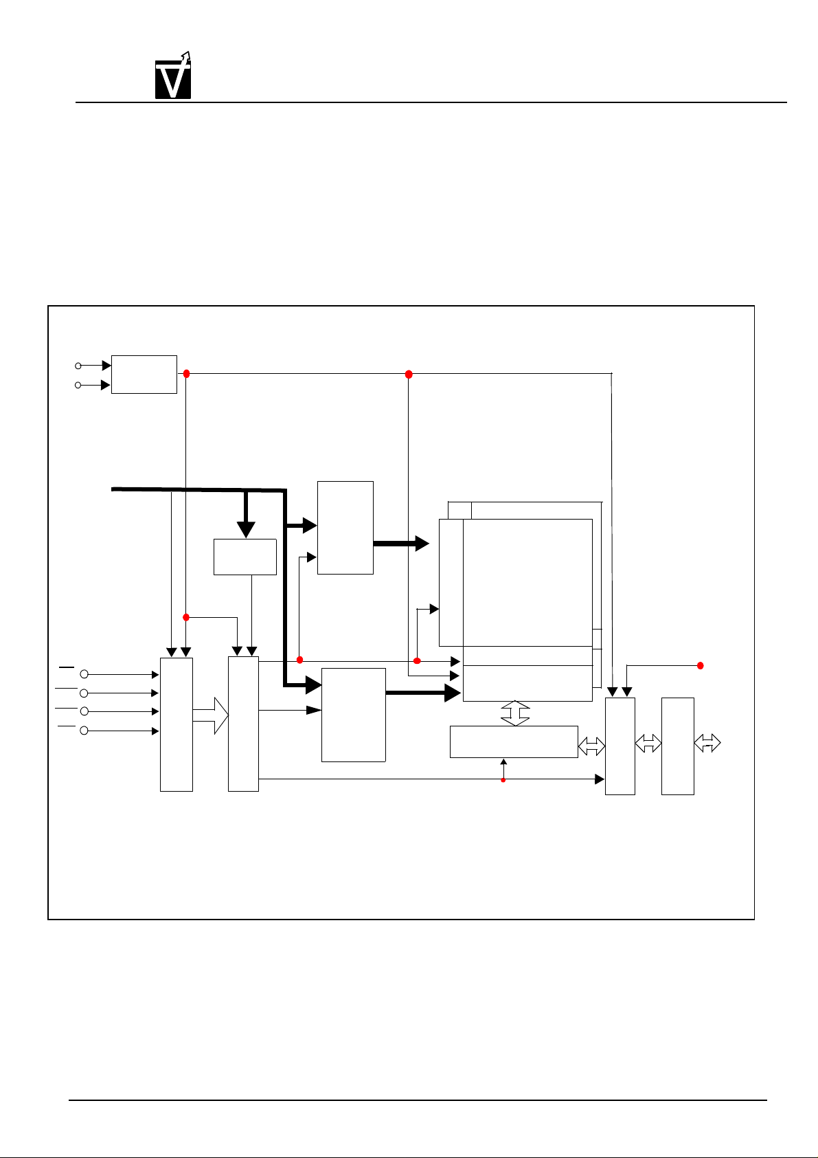
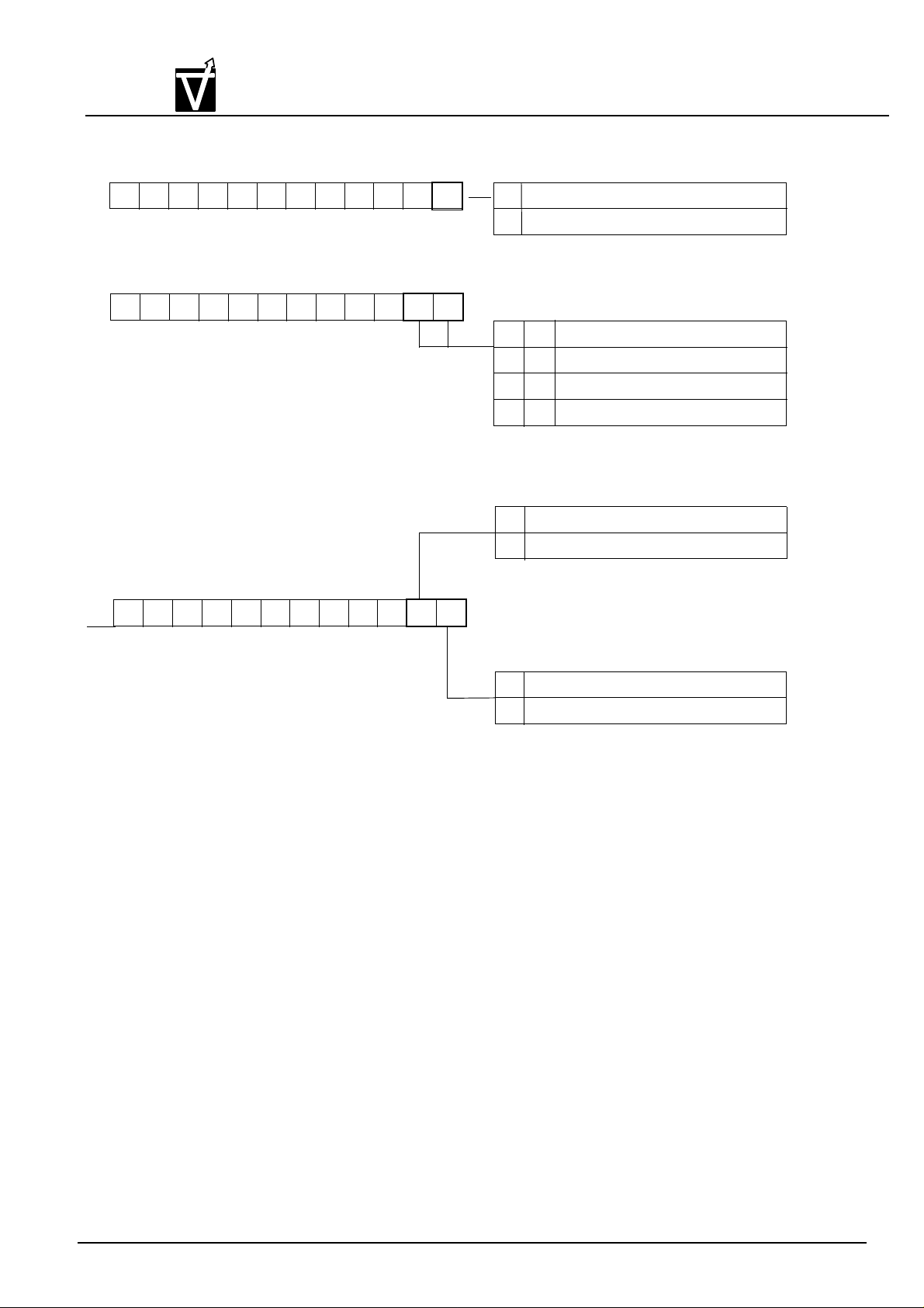
Block Diagram
VG3617161ET
1,048,576 x 16 - Bit
CMOS Synchronous Dynamic RAM
CLK
CKE
Address
CS
RAS
CAS
WE
Clock
Generator
Row
Address
Buffer
Mode
Register
Control Logic
Command Decoder
&
Refresh
Counter
Column
Address
Buffer
&
Burst
Counter
Row Decoder
Data Control Circuit DQ
Bank B
Bank A
Sense Amplifier
Column Decoder &
Latch Circuit
DQM
Buffer
Latch Circuit
Input & Output
Document:1G5-0189 Rev.1 Page 3
VIS
0VV
≤≤
µ
0VV
≤≤
µ
VG3617161ET
1,048,576 x 16 - Bit
CMOS Synchronous Dynamic RAM
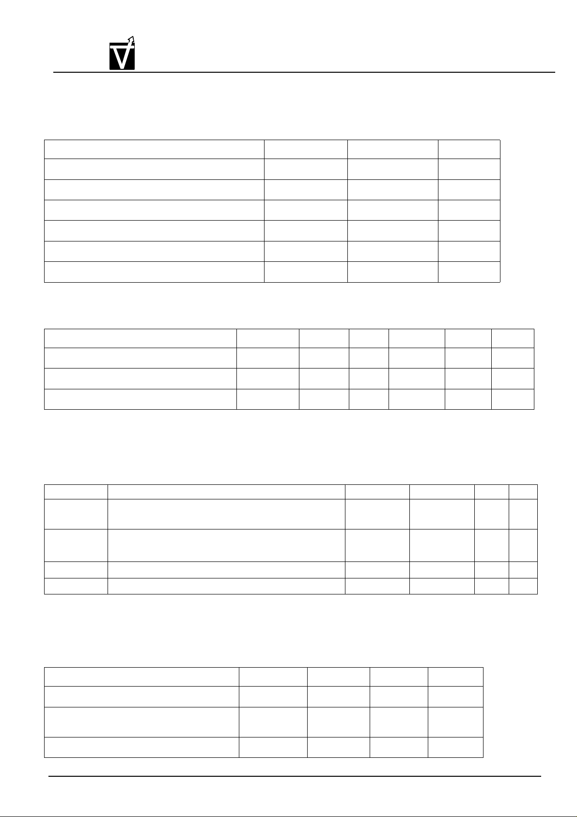
Absolute Maximum Ratings
(1)
Parameter Symbol Value Unit
Voltage on any pin relative to Vss VIN,V
Supply voltage relative to Vss VDD,V
Short circuit output current I
Power dissipation P
Operating temperature T
Storage temperature T
Recommended DC Operating Conditions (TA=0~70°C)
Parameter Symbol Min Typ Max Unit Note
Supply Voltage V
Input High Voltage, all inputs V
Input Low Voltage, all inputs V
DD
IH
IL
OUT
DDQ
OUT
D
OPT
STG
-1.0 to +4.6 V
-1.0 to +4.6 V
50 mA
1.0 W
0 to + 70 °C
-55 to + 125 °C
3.0 3.3 3.6 V
2.0 – VDD+0.3 V I
-0.3 – 0.8 V II
Note I.Overshoot limit : V
II .Undershoot limit : VIL=V
DC Electrical Characteristics
Parameter Description Min. Max. Unit Note
I
IL
I
OL
V
OH
V
OL
(All other pins not under test = 0V)
IH(MAX.)=VDDQ
SSQ
INVDD
Output disable, ()
LVTTL Output ”H” Level Voltage(l
LVTTL Output ”L” Level Voltage(l
+2.0V with a pulse width < 3ns
-2.0V with a pulse width< 3ns and -1.5V with a pulse width< 5ns
Input Leakage Current
Output Leakage Current
OUTVDDQ
= -2mA) 2.4 - V
OUT
= 2mA) - 0.4 V
OUT
-5 5 A
-5 5 A
Capacitance
(TA=25°C,f=1MHZ)
Parameter Symbol Typ Max Unit
Input capacitance(CLK) C
11
2.5 4 pF
Input capacitance(all input pins except data
C
12
2.5 5 pF
pins)
Data input/output capacitance C
Document:1G5-0189 Rev.1 Page 4
I/O
4.0 6.5 pF

VG3617161ET
±
tRCt
()
≥
CKEV
IH
≥
IH
CKEV
≥
∞
≤
CKEV
≤
CKEV
≤
∞
≤
CKEV
IH
≥
≥
CKEV
IH
≥
∞
≤
CKEV
IL
≤
CKEV
IL
≤
∞
≤
tRCtRC≥
CKE0.2V
≤
VIS
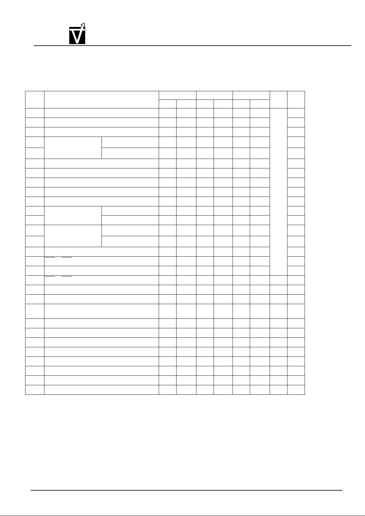
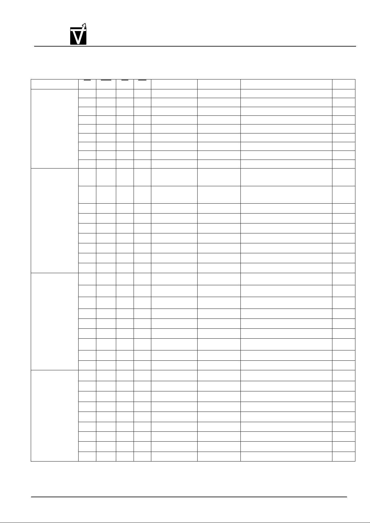
IDD Specifications (VDD = 3.3V 0.3V, TA = 0 ~ 70°C)
Description/test condition Symbol
Operating Current
RCmin
Address changed once during t
Burst length = 1 (One bank active)
Precharge Standby Current in non power-down
mode
Input signals are changed once during 2 clocks
Precharge Standby Current in non power-down
mode
Input signals are stable
Precharge Standby Current in power-down mode
, outputs open
,
CSV
(min)
, t
(min)
(max)
CK
, t
CK
IH
IL
≥
(min), tCK =tCK
CLKV
= ,
= tCK(min)
CK(min)
IL
.
(min)
(max)
I
DD1
I
DD2N
I
DD2NS
I
DD2P
1,048,576 x 16 - Bit
CMOS Synchronous Dynamic RAM
-6 -7 -8 Unit Note
Min Max Min Max Min Max
115 105 95
40 40 40 3
35 35 35
mA
2 2 2
3,4
Precharge Standby Current in power-down mode
, t
= ,
IL
(max)
CK
CLKV
IL
(max)
I
Active Standby Current in non power-down mode
(min)
, CS V
IH(min)
, t
= t
CK
CK(min)
Input signals are changed once during 2 clocks
Active Standby Current in non power-down mode
, t
= ,
(min)
CK
CLKV
IL
(max)
I
Input signals are stable
Active Standby Current in power-down mode
, t
(max)
CK = tCK(min)
Active Standby Current in power-down mode
(max)
, t
CK =
,
CLKV
IL
(max)
I
Operating Current
(Page burst, and all banks activated)
t
CCD
= t
CCD(min)
, outputs open, gapless data
Refresh Current
(t
REF
= 64ms)
(min)
Self Refresh Current I
DD2PS
I
DD3N
DD3NS
I
DD3P
DD3PS
I
DD4
I
DD5
DD6
2 2 2
50 50 50 3
40 40 40
35 35 35
35 35 35
150 140 130 4,5
100 90 80 3
1 1 1
Document:1G5-0189 Rev.1 Page 5
VIS
0.3V
±
VG3617161ET
1,048,576 x 16 - Bit
CMOS Synchronous Dynamic RAM
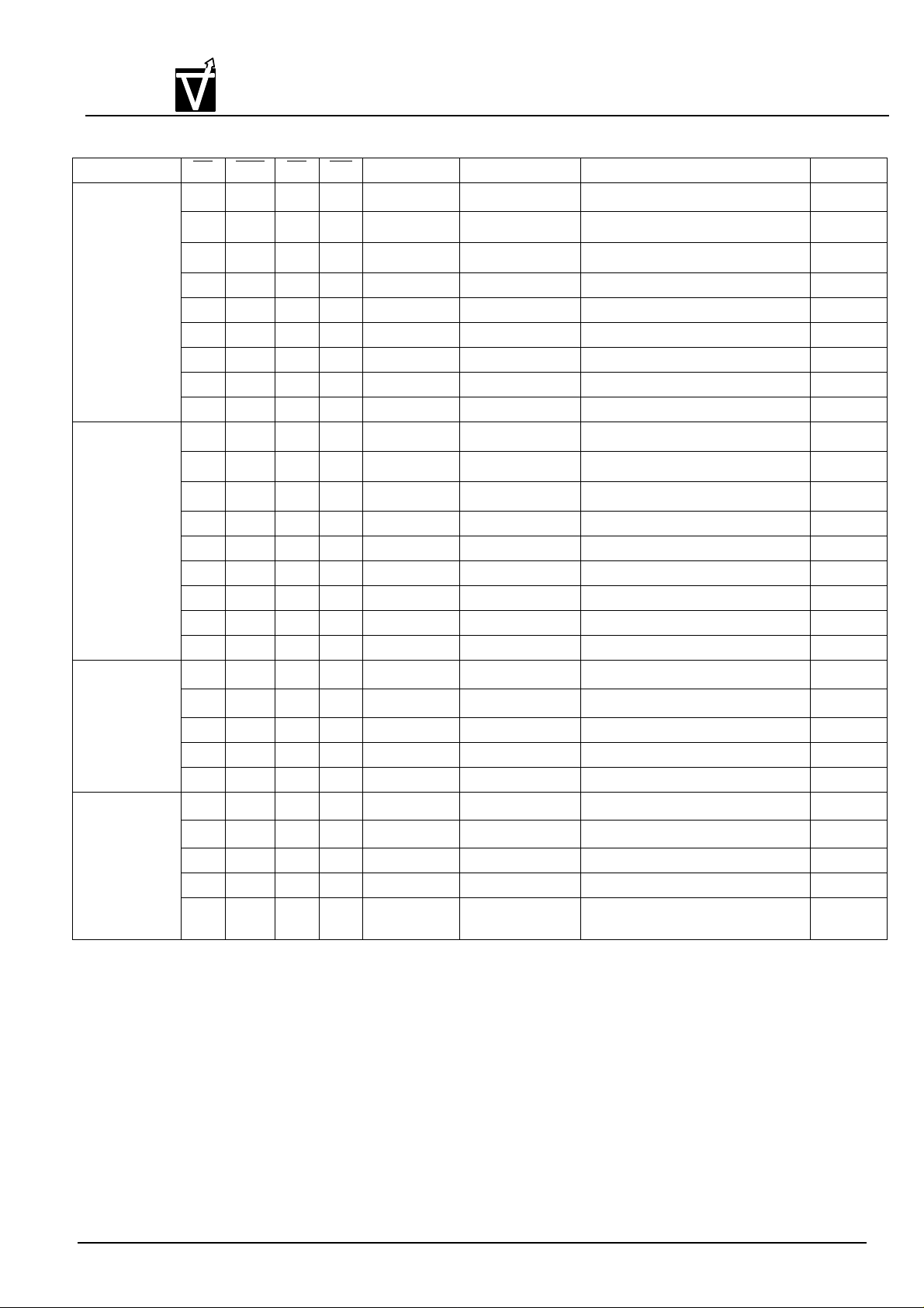
A.C Characteristics:
(6)(7)(8)(10)
(VDD=3.3V , VSS=0V, Ta=0 to 70°C)
Symbol A.C. Parameter -6 -7 -8
Unit
Note
ns
9
9
CLK
CLK
ns
CLK
CLK
CLK
ns
CLK
ms
CLK
CLK
CLK
t
CH
t
CL
t
T
t
CK3
t
CK2
t
IS
t
IH
t
DS
t
DH
t
LZ
t
HZ3
t
HZ2
t
AC3
t
AC2
t
OH
t
RCD
t
RRD
t
CCD
t
DPL
t
RAS
t
RP
t
DAL3
t
DAL2
t
RC
t
RSC
t
REF
t
SRX
t
BDL
t
PDE
Min Max Min Max Min Max
Clock high time 2.5 2.5 3
Clock low time 2.5 2.5 3
Transition time (Rise and Fall) 0.5 10 0.5 10 0.5 10
Clock cycle time CL* = 3 6 7 8
CL* = 2 8 10 12
Address/Control Input setup time 1.5 1.75 2
Address/Control Input hold time 1 1 1
Data Input setup time 1.5 1.75 2
Data Input hold time 1 1 1
Data output low impedance 1 1 1
Data output high imped-
ance
Access time from CLK
(positive edge)
Data output hold time 2.3 2.5 2.5
RAS to CAS delay 18 20 20
Row activate to row activate delay 12 14 16
CAS to CAS Delay time 1 1 1
Last data in to precharge 2 2 2
Row activate to precharge time 36 100,000 42 100,000 48 100,000
Precharge to refresh/row activate
command
Data-in to ACT (REF) Command (CL = 3) 5 5 5
Data-in to ACT (REF) Command (CL = 2) 5 5 5
Row cycle time 54 63 72
Mode Register Set Cycle time 2 2 2
Refresh time 64 64 64
Minimum CKE ”High”for Self-Refresh exit 1 1 1
Last data in to burst STOP command 1 1 1
Power Down Exit set-up time 1 1 1
CL* = 3 5.5 5.5 6
CL* = 2 6 7 7
CL* = 3 5.5 6 6
CL* = 2 6 7 7
3 3 3
Note:
1. Stresses greater than those listed under “Absolute Maximum Ratings” may cause permanent damage to the device.
2. All voltages are referenced to VSS.
3. These parameters depend on the cycle rate and these values are measured by the cycle rate under the minimum value of tCK
and tRC.
4. These parameters depend on the output loading. Specified values are obtained with the outputs open.
5. Assume minimum column address update cycle t
CCD
(min).
Document:1G5-0189 Rev.1 Page 6
VG3617161ET
VIS
6. Power-up sequence is described in Note 10.
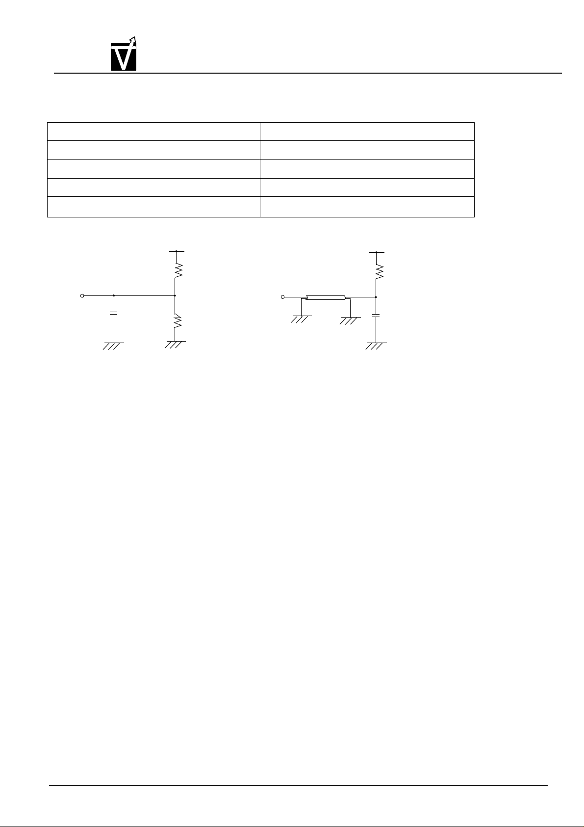
7. A.C. Test Conditions
Reference Level of Output Signals 1.4V
Output Load Reference to the Under Output Load (B)
Input Signal Levels 2.4V / 0.4V
Transition Time (Rise and Fall) of Input Signals 1ns
Reference Level of Input Signals 1.4V
1,048,576 x 16 - Bit
CMOS Synchronous Dynamic RAM
3.3V
1.2K
Ω
ZO=50
Output
30pF
LVTTL D.C. Test Load (A)
8. Transition times are measured between VIH and VIL. Transition (rise and fall) of input signals are fixed slope (1 ns).
9. tHZ defines the time at which the outputs achieve the open circuit condition and are not reference levels.
10. Power up sequence
Power up must be performed in the following sequence.
1) Power must be applied to VDD and V
CKE = ”H”, DQM = ”H”. The CLK signals must be started at the same time.
2) After power-up, a pause of 200u secouds minimum is required. Then, it is recommended that DQM is held
“high” (VDD levels) to ensure DQ output to be in the high impedance.
870
Ω
DDQ
Output
LVTTL A.C. Test Load (B)
(simultaneously) when all input signals are held “NOP” state and
Ω
1.4V
50
30pF
Ω
3) Both banks must be precharged.
4) Mode Register Set command must be asserted to initialize the Mode Register.
5) A minimum of 8 Auto-Refresh dummy cycles must be required to stabilize the internal circuitry of the device. Sequence of
4 and 5 may be changed.
Document:1G5-0189 Rev.1 Page 7
VG3617161ET
VIS
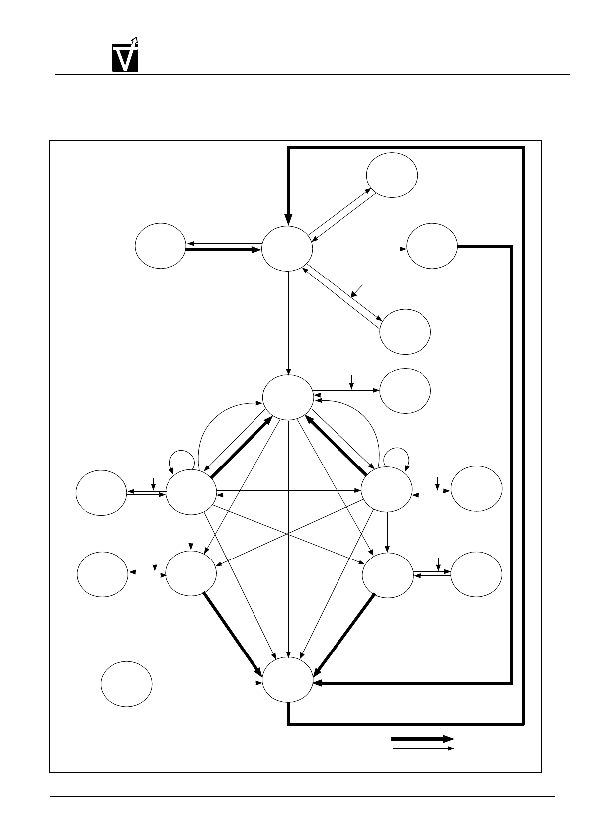
Basic Features and Function description
1.Simplified State Diagram
Mode
Register
Set
MRS
IDLE
1,048,576 x 16 - Bit
CMOS Synchronous Dynamic RAM
Self
Refresh
y
r
t
n
e
F
L
t
E
S
ACT
i
x
e
F
L
E
S
C
K
REF
C
K
E
E
AUTO
Refresh
Power
Down
WRITE
SUSPEND
WRITE A
SUSPEND
Write
CKE
CKE
Write with
Auto Precharge
CKE
CKE
WRITE A
WRITE
B
S
T
READ
READ A
Active
Power
Down
Read
CKE
CKE
Read with
Auto Precharge
CKE
CKE
READ
SUSPEND
READ A
SUSPEND
ROW
ACTIVE
T
S
B
rite
W
A
u
t
P
R
E
(
P
r
h
t
i
w
h
e
t
d
i
r
e
r
W
p
o
t
u
A
Read
R
e
a
d
w
o
i
P
t
h
r
e
c
h
a
r
g
e
e
c
h
a
r
g
e
t
e
r
m
i
n
a
t
i
o
n
)
A
e
g
r
a
PRE
Write
A
CKE
CKE
Re
R
u
e
t
o
P
r
e
c
a
e
R
o
t
u
(
E
R
P
ad
a
d
w
i
t
h
h
a
r
g
e
h
e
t
i
g
w
r
a
d
h
c
e
r
P
)
n
o
i
t
a
n
i
m
r
e
t
e
g
r
a
h
c
e
r
P
POWER
ON
Precharge
Precharge
Automatic sequence
Manual input
Note: After the AUTO refresh operation, precharge operation is
performed automatically and enter the IDLE state
Document:1G5-0189 Rev.1 Page 8
VG3617161ET
VIS
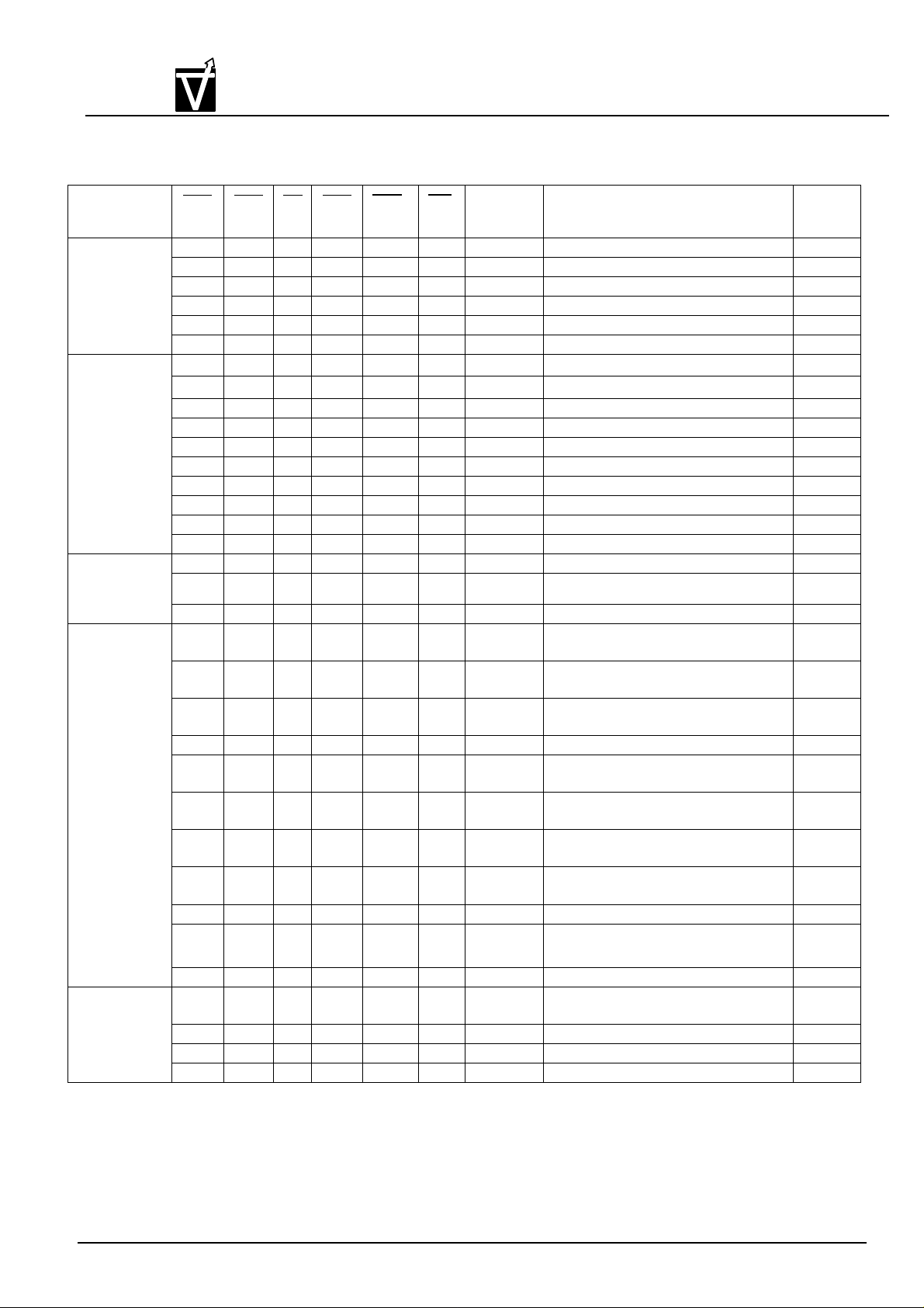
2.Truth Table
2.1 Command Truth Table
1,048,576 x 16 - Bit
CMOS Synchronous Dynamic RAM
CKE
FUNCTION Symbol
n-1 n
CS RAS CAS WE A11 A10
Device deselect DESL H X H X X X X X X
No operation NOP H X L H H H X X X
Mode register set MRS H X L L L L L L V
Bank activate ACT H X L L H H
Read READ H X L H L H
Read with auto precharge READA H X L H L H
Write WRIT H X L H L L
Write with auto precharge WRITA H X L H L L
Precharge select bank PRE H X L L H L
BS
BS
BS
BS
BS
BS
(2)
Row Row
(2)
(2)
(2)
(2)
(2)
L
H
L
H
L X
Precharge all banks PALL H X L L H L X H X
Burst stop BST H X L H H L X X X
Note: (1) Column address: A0~A7
(2) BS: Bank Select. L means Bank A and H means Bank B.
2.2 DQM Truth Table
CKE DQM
FUNCTION Symbol
n-1 n-1 UDQM LDQM
Data write/output enable ENB H X L
Data mask/output disable MASK H X H
Upper byte write enable/output enable ENBU H X L X
Lower byte write enable/output enable ENBL H X X L
Upper byte write inhibit/output disable MASKU H X H X
Lower byte inhibit/output disable MASKL H X X H
A9-
A0
Col
Col
Col
Col
(1)
(1)
(1)
(1)
2.3 CKE Truth Table
Current State Function Symbol
CKE
n-1 n
CS RAS CAS WE
Add-
ress
Activating Clock suspend mode entry H L X X X X X
Any Clock suspend L L X X X X X
Clock suspend Clock suspend mode exit L H X X X X X
Idle CBR refresh command REF H H L L L H X
Idle Self refresh entry SELF H L L L L H X
Self refresh Self refresh exit L H L H H H X
L H H X X X X
Idle Power down entry H L X X X X X
Power down Power down exit L H X X X X X
H : High level, L : Low level, X : high or Low level(Don’t care), V : Valid Data input
Document:1G5-0189 Rev.1 Page 9
VG3617161ET
endRow
→
endRow
→
stopRow
→
endwrite
→
endWrite
→
stopRow
→
1,048,576 x 16 - Bit
VIS
2.4 Operative Command Table
Current state CS RAS CAS WE Address Command Action Notes
Idle H X X X X DESL Nop or Power down 2
L H H X X NOP or BST Nop or Power down 2
L H L H BA,CA,A10 READ/READA ILLEGAL 3
L H L L BA,CA,A10 WRIT/WRITA ILLEGAL 3
L L H H BR,RA ACT Row active
L L H L BA,A10 PRE/PALL Nop
L L L H X REF/SELF Refresh or Self refresh 4
L L L L Op-Code MPS Mode register access
Row active H X X X X DESL Nop
L H H X X NOP or BST Nop
L H L H BA,CA,A10 READ/READA Begin read:Determine AP 5
L H L L BA,CA,A10 WRIT/WRITA Begin write:Determine AP 5
L L H H BA,RA ACT ILLEGAL 3
L L H L BA,A10 PRE/PALL Precharge 6
L L L H X REF/SELF ILLEGAL
L L L L Op-Code MRS ILLEGAL
Read H X X X X DESL
CMOS Synchronous Dynamic RAM
(1/3)
Continue burst to active
L H H H X NOP
L H H L X BST
L H L H BA,CA,A10 READ/READA Term burst, new read:Determine AP 7
L H L L BA,CA,A10 WRIT/WRITA Term burst, start write:Determine AP 7,8
L L H H BA,RA ACT ILLEGAL 3
L L H L BA,A10 PRE/PALL Term burst,precharging
L L L H X REF/SELF ILLEGAL
L L L L Op-Code MRS ILLEGAL
Write H X X X X DESL
L H H H X NOP
L H H L X BST
L H L H BA,CA,A10 READ/READA Term burst, start read: determine AP 7,8
L H L L BA,CA,A10 WRIT/WRITA Term burst, new write:Determine AP 7
L L H H BA,RA ACT ILLEGAL 3
L L H L BA,A10 PRE/PALL Term burst precharging 9
L L L H X REF/SELF ILLEGAL
L L L L Op-Code MRS ILLEGAL
Continue burst to active
Burst active
Continue burst to recovering
Continue burst to recovering
Burst active
Document:1G5-0189 Rev.1 Page 10
VG3617161ET
endPreching
arg→endPreching
arg
→
endWrite
→
endWrite
→
NopEnter
→
NopEnter
→
NopEnter
→
NopEnter
→
NopEnter
→
NopEnter
→
NopEnter
→
1,048,576 x 16 - Bit
VIS
Current state CS RAS CA WE Address Command Action Notes
Read with auto
precharge
Write with auto
precharge
Precharging H X X X X DESL
Row activating H X X X X DESL
H X X X X DESL
L H H H X NOP
L H H L X BST ILLEGAL
L H L H BA,CA,A10 READ/READA ILLEGAL
L H L L BA,CA,A10 WRIT/WRITA ILLEGAL
L L H H BA,RA ACT ILLEGAL 3
L L H L BA,A10 PRE/PALL ILLEGAL 3
L L L H X PEF/SELF ILLEGAL
L L L L Op-Code MRS ILLEGAL
H X X X X DESL
L H H H X NOP
L H H L X BST ILLEGAL
L H L H BA,CA,A10 READ/READA ILLEGAL
L H L L BA,CA,A10 WRIT/WRITA ILLEGAL
L L H H BA,RA ACT ILLEGAL 3
L L H L BA,A10 PRE/PALL ILLEGAL 3
L L L H X REF/SELF ILLEGAL
L L L L Op-code MRS ILLEGAL
L H H H X NOP
L H H L X BST
L H L H BA,CA,A10 READ/READA ILLEGAL 3
L H L L BA,CA,A10 WRIT/WRITA ILLEGAL 3
L L H H BA,RA ACT ILLEGAL 3
L L H L BA,A10 PRE/PALL
L L L H X REF/SELF ILLEGAL
L L L L Op-Code MRS ILLEGAL
L H H H X NOP
L H H L X BST
L H L H BA,CA,A10 READ/READA ILLEGAL 3
L H L L BA,CA,A10 WRIT/WRITA ILLEGAL 3
L L H H BA,RA ACT ILLEGAL 3,10
L L H L BA,A10 PRE/PALL ILLEGAL 3
L L L H X REF/SELF ILLEGAL
L L L L Op-Code MRS ILLEGAL
CMOS Synchronous Dynamic RAM
(2/3)
Continue burst to
Continue burst to
Continue burst to
recovering with auto precharge
Continue burst to
recovering with auto precharge
idle after t
idle after t
idle after t
idle after t
row active after t
row active after t
row active after t
RP
RP
RP
RP
RCD
RCD
RCD
Document:1G5-0189 Rev.1 Page 11
VG3617161ET
NopEnter
→
NopEnter
→
NopEnter
→
NopEnter
→
NopEnter
→
NopEnter
→
NopEnter
→
NopEnter
→
NopEnter
→
NopEnter
→
1,048,576 x 16 - Bit
VIS
Current state CS RAS CA WE Address Command Action Notes
Write
recovering
Write
recovering
with auto
precharge
Refreshing H X X X X DESL
Mode register
accessing
H X X X X DESL
L H H H X NOP
L H H L X BST
L H L H BA,CA,A10 READ/READA Start read, Determine AP 8
L H L L BA,CA,A10 WRIT/WRITA New write, Determine AP
L L H H BA,RA ACT ILLEGAL 3
L L H L BA,A10 PRE/PALL ILLEGAL 3
L L L H X PEF/SELF ILLEGAL
L L L L Op-Code MRS ILLEGAL
H X X X X DESL
L H H H X NOP
L H H L X BST
L H L H BA,CA,A10 READ/READA ILLEGAL 3,8
L H L L BA,CA,A10 WRIT/WRITA ILLEGAL 3
L L H H BA,RA ACT ILLEGAL 3
L L H L BA,A10 REF/PALL ILLEGAL 3
L L L H X REF/SELF ILLEGAL
L L L L Op-Code MRS ILLEGAL
L H H X X NOP/BST
L H L X X READ/WRIT ILLEGAL
L L H X X ACT/PRE/PALL ILLEGAL
L L L X X REF/SELF/MRS ILLEGAL
H X X X X DESL
L H H H X NOP
L H H L X BST ILLEGAL
L H L X X READ/WRITE ILLEGAL
L L X X X ACT/PRE/PALL/
REF/SELF/MRS
CMOS Synchronous Dynamic RAM
(3/3)
row active after t
row active after t
row active after t
precharge after t
precharge after t
precharge after t
idle after t
idle after t
idle after 2 Clocks
idle after 2 Clocks
ILLEGAL
RC
RC
DPL
DPL
DPL
DPL
DPL
DPL
Note 1. All entries assume that CKE was active (High level)during the preceding clock cycle.
2. If both banks are idle, and CKE is inactive(Low level), the device will enter Power down mode.
All input buffers except CKE will be disabled.
3. Illegal to bank in specified states; Function may be legal in the bank indicated by Bank Address (BA),
depending on the state of that bank.
4. If both banks are idle, and CKE is inactive(Low level), the device will enter Self refresh mode.
All input buffers except CKE will be disabled.
5. IIIegal if t
6. IIIegal if t
7. Must satisfy burst interrupt condition.
8. Must satisfy bus contention, bus turn around, and/or write recovery requirements.
9. Must mask preceding data if t
10. IIIegal if t
is not satisfied.
RCD
is not satisfied.
RAS
is not satisfied.
RRD
is not satisfied.
DPL
Document:1G5-0189 Rev.1 Page 12
VG3617161ET
PDIdle
→
VIS
2.5 Command Truth Table for CKE
1,048,576 x 16 - Bit
CMOS Synchronous Dynamic RAM
Current state
Self refresh
(SR)
Self refresh
recovery
Power down
(PD)
Both banks
idle
Any state
other than
listed above
CKE
RASnCS RAS
n-1
H X X X
L H H X
L H L H
L H L H
L H L L
L L X X
H H H X
H H L H
H H L H
H H L L
H L H X
H L L H
H L L H
H L L L
L H X X
L L X X
H X X X
L H X X
L L X X
H H H X
H H L H
H H L L
H H L L
H H L L
H L H X
H L L H
H L L L
H L L L
H L L L
L X X X
H H X X
H L X X
L H X X
L L X X
CAS WE Address Action Notes
X X X INVALID,CLK(n-1)would exit S.R.
X X X SR Recovery 2
H X X SR Recovery 2
L X X ILLEGAL 2
X X X ILLEGAL 2
X X X Maintain S.R.
X X X Idle after t
H X X Idle after t
RC
RC
L X X ILLEGAL
X X X ILLEGAL
X X X Begin clock suspend next cycle 5
H X X Begin clock suspend next cycle 5
L X X ILLEGAL
X X X ILLEGAL
X X X Exit clock suspend next cycle 2
X X X Maintain clock suspend
X X INVALID, CLK(n-1) would exit P.D.
X X X
EXIT
2
X X X Maintain power down mode
X X Refer to operations in Operative
Command Table
X X Refer to operations in Operative
Command Table
H X Refer to operation in Operative
Command Table
L H X Refresh
L L Op-
Code
Refer to operations in Operative
Command Table
X X Refer to operations in Operative
Command Table
X X Refer to operations in Operative
Command Table
H X Refer to operations in Operative
Command Table
L H X Self refresh 3
L L Op-
Code
Refer to operations in Operative
Command Table
X X X Power down 3
X X X Refer to operations in Operative
Command Table
X X X Begin clock suspend next cycle 4
X X X Exit clock suspend next cycle
X X X Maintain clock suspend
Note 1. H : Hight level, L : low level, X : High or low level(Don't care).
2. CKE Low to High transition will re-enable CLK and other inputs asynchronously. A minimum setup time must be satisfied
before any command other than EXIT.
3. Power down and Self refresh can be entered only from the both banks idle state.
4. Must be legal command as defined in Operative Command Table.
5 .IIIegal if t
Document:1G5-0189 Rev.1 Page 13
is not satisfied.
SRX

VG3617161ET
1,048,576 x 16 - Bit
VIS
3.Initiallization
The synchronous DRAM is initialized in the power on sequence. Once power has been applied, a
200us minimum delay is needed in which stable power and input signals are maintained. During this delay,
CKE and DQM recommend to be held high.
After the 200us delay, both banks must be precharged using the precharge command. Once precharge
is completed and the minimum tRP is satisfied, the mode register can be programmed.
Minimum 8 CBR refresh cycles must be performed before or after the mode register set command.
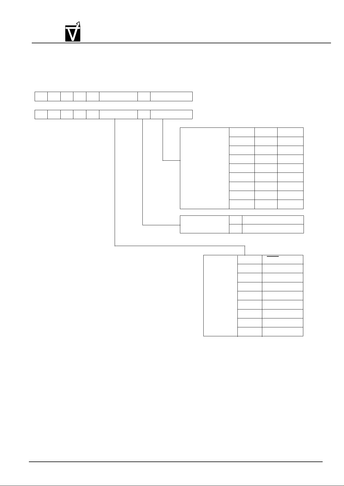
4.Programming the Mode Register
The mode register is programmed by the mode register set command using address bits A11 through
A0 as data inputs. The register retains data until it is reprogrammed or until the device loses power.
The mode register has four fields;
Options : A11 through A7
CAS latency : A6 through A4
Wrap type : A3
Burst length : A2 through A0
Following mode register programming, no command can be asserted befor at least two clock cycles
have elapsed.
CMOS Synchronous Dynamic RAM
CAS Latency
CAS latency is the most critical parameter to be set. It tells the device how many clocks must elapse
before the data will be available. The SDRAM is capable of reconfiguring its internal architecture based
on the value of CAS latency.
The value is determined by the frequency of the clock and the speed grade of the device. The value
can be programmed as 2 or 3.
Burst Length
Burst Length is the number of words that will be output or input in read or write cycle. After a read burst
is completed, the output bus will become high impedance.
The burst length is programmable as 1,2,4,8 or full page.
Wrap Type (Burst Sequence)
The wrap type specifies the order in which the burst data will be addressed. The order is programmable
as either “Sequential” or “Interleave”. The method chosen will depend on the type of CPU in the system.
Some microprocessor cache systems are optimized for sequential addressing and others for interleaved addressing. Both sequences support bursts of 1,2,4 and 8. Only the sequential burst. supports the
full-page length.
Document:1G5-0189 Rev.1 Page 14
VIS
5.Mode Register
VG3617161ET
1,048,576 x 16 - Bit
CMOS Synchronous Dynamic RAM
11
0 0
11
0
10
10
0
8
9
1
9
0
0 0
8
0 0
7
7
5
6
LTMODE
5
6
LTMODE
3
4
WT
3
4
WT
1
2
2
BL
BL
0
Burst Read and Single Write
1
0
Mode Register Set
Burst length
Wrap type
X=Don’t care
Bits2-0
000
001
010
011
100
101
110
111
01Sequential
Interleave
WT=0
1
2
4
8
R
R
R
Full page
WT=1
1
2
4
8
R
R
R
R
Latency
mode
Remark R:Reserved
Bits6-4
000
001
010
011
100
101
110
111
CAS Iatency
R
R
2
3
R
R
R
R
Document:1G5-0189 Rev.1 Page 15
VG3617161ET
VIS
5.1 Burst Length and Sequence
(Burst Length= 2)
1,048,576 x 16 - Bit
CMOS Synchronous Dynamic RAM
Starting Address
(column address A0, binary)
0 0,1 0,1
1 1,0 1,0
(Burst Length=4)
Starting Address
(column address A1-A0, binary)
00 0,1,2,3 0,1,2,3
01 1,2,3,0 1,0,3,2
10 2,3,0,1 2,3,0,1
11 3,0,1,2 3,2,1,0
(Burst Length=8)
Starting Address
(column address A2-A0, binary)
Sequential Addressing
Sequence (decimal)
Sequential Addressing
Sequence (decimal)
Sequential Addressing
Sequence (decimal)
Interleave Addressing
Sequence(decimal)
Interleave Addressing
Sequence(decimal)
Interl
eave Addressing
Sequence(decimal)
000 0,1,2,3,4,5,6,7 0,1,2,3,4,5,6,7
001 1,2,3,4,5,6,7,0 1,0,3,2,5,4,7,6
010 2,3,4,5,6,7,0,1 2,3,0,1,6,7,4,5
011 3,4,5,6,7,0,1,2 3,2,1,0,7,6,5,4
100 4,5,6,7,0,1,2,3 4,5,6,7,0,1,2,3
101 5,6,7,0,1,2,3,4 5,4,7,6,1,0,3,2
110 6,7,0,1,2,3,4,5 6,7,4,5,2,3,0,1
111 7,0,1,2,3,4,5,6 7,6,5,4,3,2,1,0
Full page burst is an extension of the above tables of sequential addressing, with the length being 256
words.
Document:1G5-0189 Rev.1 Page 16
VG3617161ET
VIS
6.Address Bits of Bank-Select and Precharge
1,048,576 x 16 - Bit
CMOS Synchronous Dynamic RAM
A0
Row
(Activate command)
A0
Row
(Precharge)
A0
Col.
(CAS strobes)
A2A1
A2A1
A2A1
A3
A3
A3
A4
A4
A4
A5
A5
A5
A6
A6
A6
A7
A7
A7
A8
A8
A8
A9
A9
A9
A10
A10
A10
A11
A11
A11
0
Select Bank A ”Activate” command
1
Select Bank B ”Activate” command
Result
A11
A10
0
0
0
1
0
1
Precharge Bank A
1
Precharge Bank B
x
Precharge All Banks
x:Don’t care
Disable Auto-Precharge (End of Burst)
Enable Auto-Precharge (End of Burst)
Enable Read/Write commands for Bank A
0
Enable Read/Write commands for Bank B
1
Document:1G5-0189 Rev.1 Page 17
VIS
7.PRECHARGE
VG3617161ET
1,048,576 x 16 - Bit
CMOS Synchronous Dynamic RAM
The PRECHARGE command can be asserted anytime after t
RAS(min)
is satisfied.
Soon after the PRECHARGE command is asserted, PRECHARGE operation is performed. The synchronous DRAM
enters the idle state after t
is satisfied. The parameter tRP is the time required to perform the PRECHARGE.
RP(min)
The earliest timing in a READ cycle that a PRECHARGE command can be asserted without losing any data in the
burst is as followed.
PRECHARGE
CLK
Command
CAS latency=2
DQ
Command
CAS latency=3
T0 T1
Read
Read
T2
T3
Q0 Q3Q2
T4 T5
PRE
Q1
PRE
T6
Hi-Z
Burst lengh=4
T7
DQ
CAS latency=
2: One clock earlier than the last output data.
3: Two clocks earlier than the last output data.
In order to write all data to the memory cell correctly, the asynchronous parameter”t
The t
DPL(MIN.)
cycle. The minimum number of clocks are calculated by dividing t
specification defines the earliest time that a PRECHARGE command can be asserted after a WRITE
DPL(min.)
Q0
Q1
” must be satisfied.
DPL
by the clock cycle time.
Q2
In summary, the PRECHARGE command can be asserted relative to the reference clock of the last valid
data. In the following table, minus means clocks before the reference, plus means time after the reference.
CAS latency READ WRITE
2 -1 +t
DPL(min.)
Q3
(t
RAS
Hi-Z
is satisfied)
3 -2 +t
DPL(min)
Document:1G5-0189 Rev.1 Page 18
VG3617161ET
1,048,576 x 16 - Bit
VIS
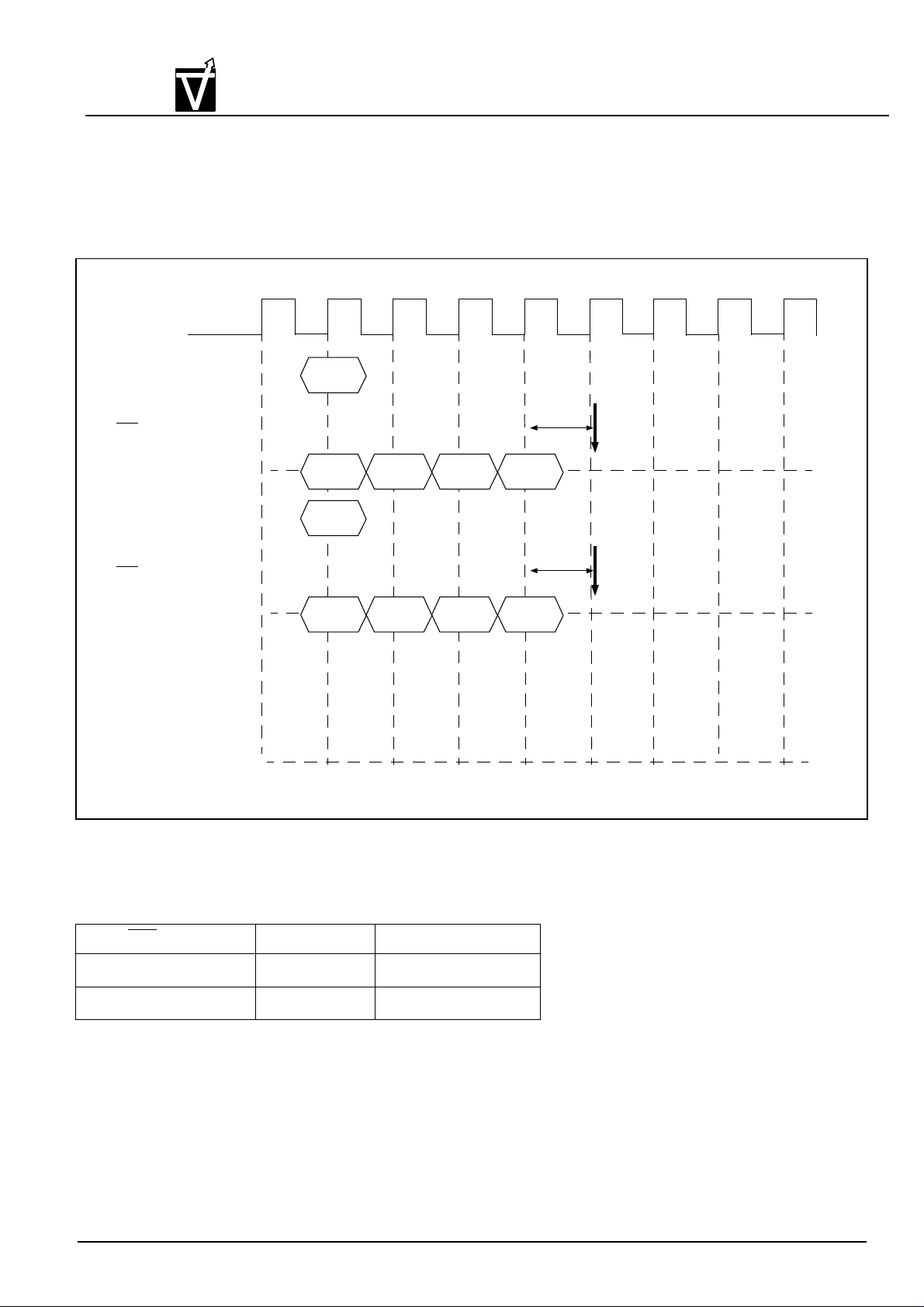
8.AUTO PRECHARGE
During a READ or WRITE command cycle, A10 controls whether AUTO PRECHARGE is selected. If A10 is
high in the READ or WRITE command (READ with AUTO PRECHARGE command or WRITE with AUTO PRECHARGE command), AUTO PRECHARGE is selected and precharging begins automatically after the burst
access.
In the WRITE cycle, t
DAL(min.)
charged.
When using AUTO PRECHARGE in the READ cycle, knowing when the PRECHARGE starts is important
because the t
be asserted after t
must be satisfied. Once AUTO PRECHARGE has started, an active command to the bank can
RAS
has been satisfied.
RP(min.)
The timing at which the AUTO PRECHARGE cycle begins depends both on the CAS Iatency programmed
into the mode register and on whether the cycle is READ or WRITE.
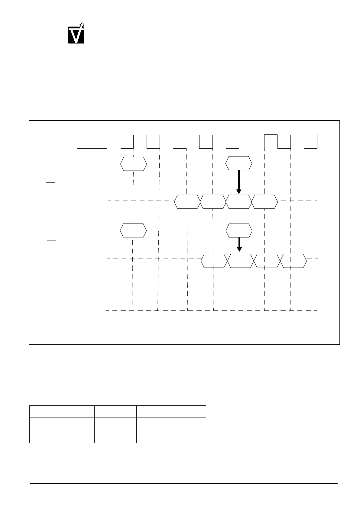
8.1 READ with AUTO PRECHARGE
During a READA cycle, the AUTO PRECHARGE begins one clock earlier(CAS Iatency of 2) or two
clocks earlier(CAS Iatency of 3) than the last data word output.
must be satisfied to assert the next active command to the bank being pre-
CMOS Synchronous Dynamic RAM
READ with AUTO PRECHARGE
CLK
Command
CAS latency=2
DQ
Command
CAS latency=3
DQ
T0 T1
READA B
READA B
Burst lengh=4
QB0
T3
QB1
QB0
QB0 QB1
T4 T5
Auto precharge starts
Auto precharge starts
T2
T6
QB3QB2
QB2QB1
QB3
T7
Hi-Z
Hi-Z
T8
Remark: READA means READ with AUTO PRECHARGE
Document:1G5-0189 Rev.1 Page 19
VG3617161ET
VIS
8.2 WRITE with AUTO PRECHARGE
During a WRITA cycle, the AUTO PRECHARGE starts at t
the device
WRITE with AUTO PRECHRGE
T0 T1
CLK
1,048,576 x 16 - Bit
CMOS Synchronous Dynamic RAM
DPL(min.)
T2
T3
after the last data word input to
T4 T5
T6
Burst lengh=4
T7
T8
Command
CAS latency=2
DQ
Command
CAS latency=3
DQ
Remark WRITA means WRITE with AUTO PRECHARGE
WRITA B
DB0
WRITA B
DB0
DB1
DB1
AUTO PRECHARGE starts
t
DPL
DB3DB2
AUTO PRECHARGE starts
t
DPL
DB3DB2
Hi-Z_
Hi-Z_
In summary, the auto precharge cycle begins relative to a reference clock that indicates the last data word is
valid.
In the table below, minus means clocks before the reference; plus means clocks after the reference.
CAS latency READ WRITE
2 -1 +t
3 -2 +t
DPL(min.)
DPL(min)
Document:1G5-0189 Rev.1 Page 20
VG3617161ET
VIS
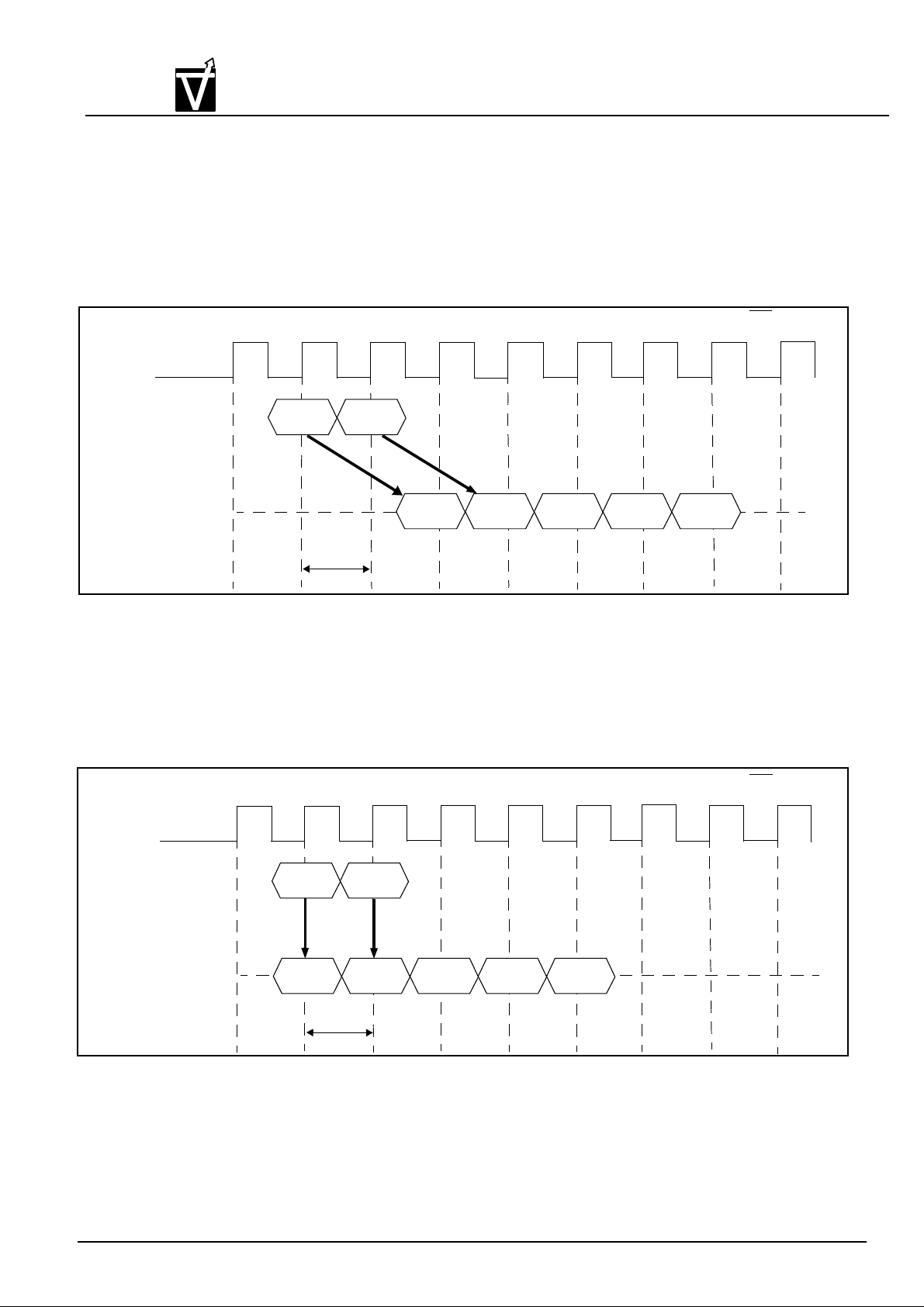
9.READ/WRITE Command Interval
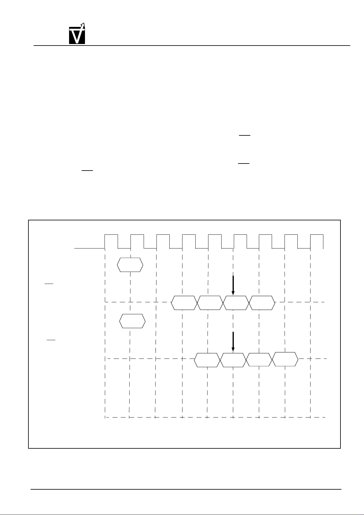
9.1 READ to READ command interval
When a new READ command is asserted during a READ cycle, it will be effective after the CAS latency,
even if the previous READ operation has not completed. READ will be interrupted by another READ.
A READ command can be asserted in every clock without restriction.
READ to READ Command Interval
CLK
T0 T1
T2
T3
CMOS Synchronous Dynamic RAM
T4 T5
1,048,576 x 16 - Bit
Burst lengh=4, CAS latency=2
T6
T7
T8
1 cycle
Read B
QA0
QB0
QB2QB1
Command
DQ
Read A
9.2 WRITE to WRITE Command Interval
When a new WRITE command is asserted during a WRITE cycle, the previous burst will be terminated
and the new burst will begin with the new WRITE command. WRITE will be interrupted by another WRITE.
A WRITE command can be asserted in every clock without restriction.
WRITE to WRITE Command Interval
Burst lengh=4, CAS latency=2
CLK
T0 T1
T2
T3
T4 T5
T6
QB3
Hi-Z_
T7
T8
1 cycle
Write B
QB0
QB2QB1
QB3
Hi-Z_
Command
DQ
Write A
QA0
Document:1G5-0189 Rev.1 Page 21
 Loading...