

VIS VG26S18165CJ-5, VG26S18165CJ-6, VG26V18165CJ-6, VG26V18165CJ-5 Datasheet

VG26(V)(S)18165C
10±
10±
1,048,576 x 16 - Bit
VIS
Description
The device CMOS Dynamic RAM organized as 1,048,576 words x 16 bits with extended data out access
mode. It is fabricated with an advanced submicron CMOS technology and designed to operate from a single
5V only or 3.3V oniy power supply. Low voltage operation is more suitable to be used on battery backup,
portable electronic application. A new refresh feature called “self-refresh” is supported and very slow CBR
cycles are being performed. lt is packaged in JEDEC standard 42-pin plastic SOJ.
Features
• Single 5V(%) or 3.3V(%) only power supply
CMOS Dynamic RAM
• High speed t
• Low power dissipation
- Active wode : 5V version 660/605 mW (Mas)
3.3V version 432/396 mW (Mas)
- Standby mode: 5V version 1.375 mW (Mas)
3.3V version 0.54 mW (Mas)
• Extended - data - out(EDO) page mode access
• I/O level: TTL compatible (Vcc = 5V)
LVTTL compatible (Vcc = 3.3V)
• 1024 refresh cycle in 16 ms(Std.) or 128 ms(S-version)
• 4 refresh modes:
- RAS only refresh
- CAS - before - RAS refresh
- Hidden refresh
- Self-refresh(S-version)
acess time: 50/60ns
RAC
Document:1G5-0147 Rev.1 Page 1
VIS
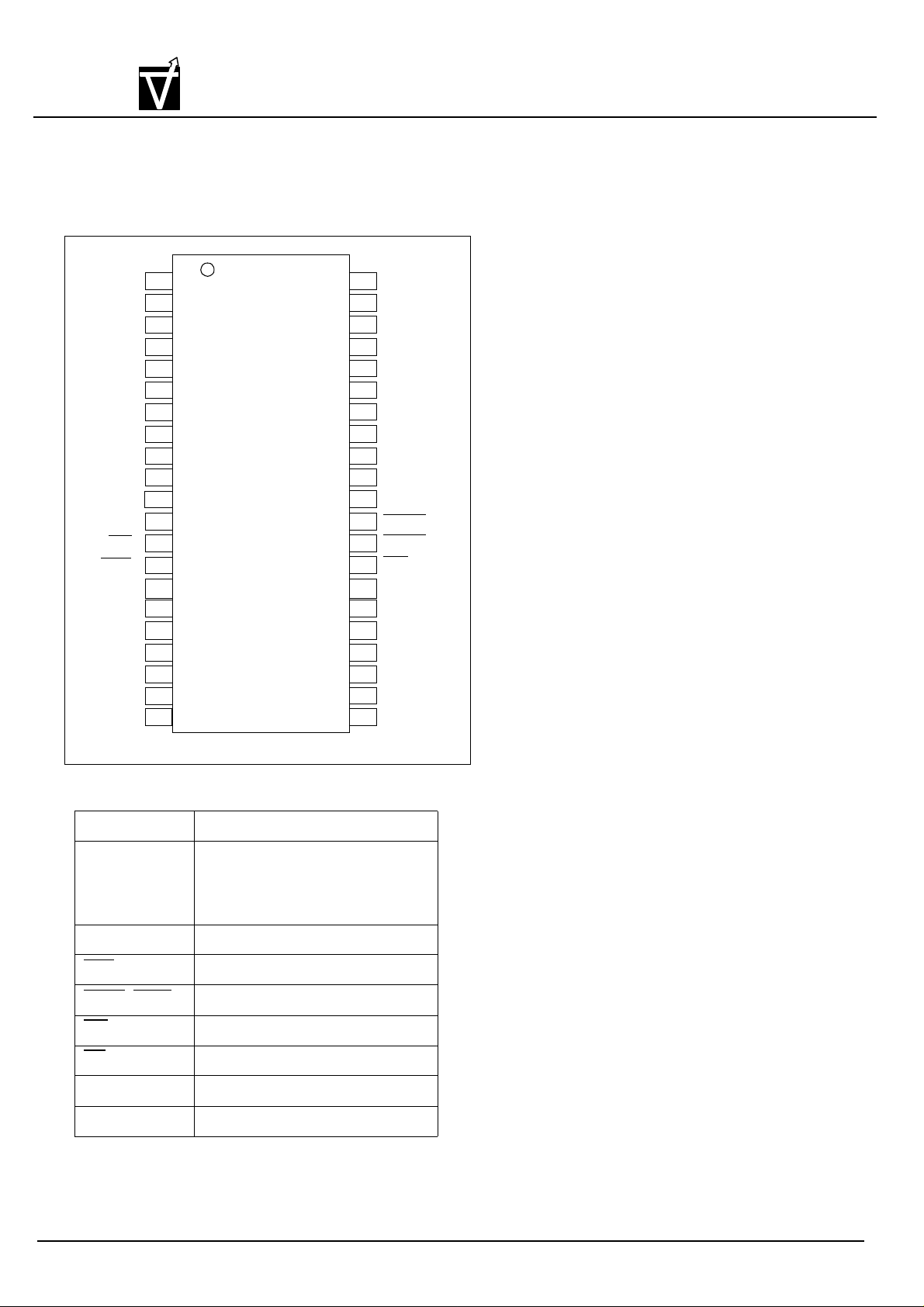
Pin Configuration
42-Pin 400mil Plastic SOJ
VG26(V)(S)18165C
1,048,576 x 16 - Bit
CMOS Dynamic RAM
VCC
DQ1
DQ2
DQ3
DQ4
VCC
DQ5
DQ6
DQ7
DQ8
NC
NC
WE
RAS
NC
NC
A0
A1
A2
A3
VCC
5
6
7
8
9
10
11
12
13
14
15
16
17
18
19
20
21
1
2
3
4
VG26(V)(S)18165CJ
42
41
40
39
38
37
36
35
34
33
32
31
30
29
28
27
26
25
24
23
22
VSS
DQ16
DQ15
DQ14
DQ13
VSS
DQ12
DQ11
DQ10
DQ9
NC
LCAS
UCAS
OE
A9
A8
A7
A6
A5
A4
VSS
Pin Description
Pin Name Function
A0-A9 Address inputs
- Row address
- Column address
- Refresh address
DQ1~DQ16 Data-in / data-out
RAS Row address strobe
UCAS, LCAS Column address strobe
WE Write enable
OE Output enable
Vcc Power (+5 V or + 3.3V)
Vss Ground
A0-A9
A0-A9
A0-A9
Document:1G5-0147 Rev.1 Page 2
VIS
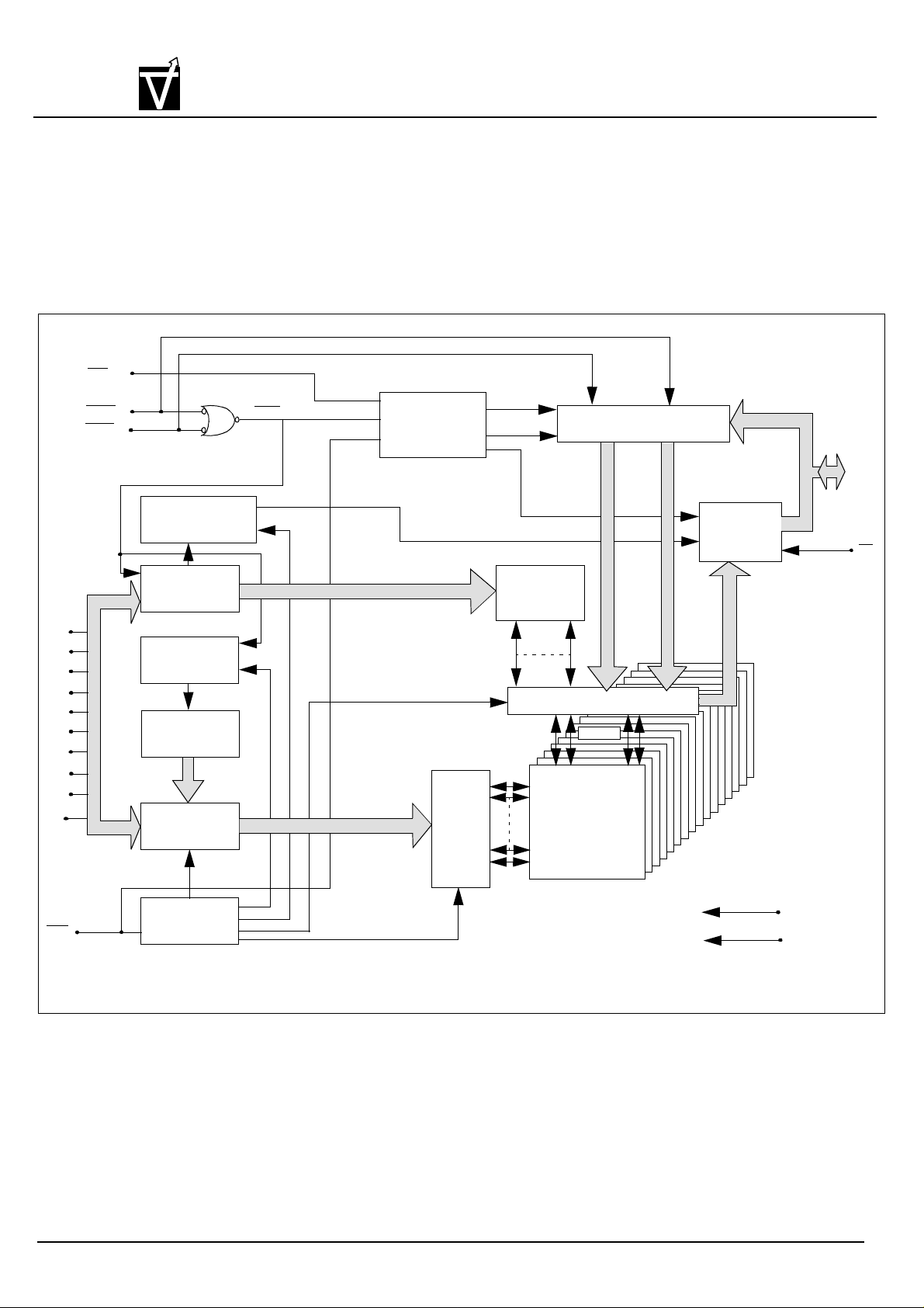
Block Diagram
WE
VG26(V)(S)18165C
1,048,576 x 16 - Bit
CMOS Dynamic RAM
A9
A0
A1
A2
A3
A4
A5
A6
A7
A8
LCAS
UCAS
NO.2 CLOCK
GENERATOR
COLUMN-
ADDRESS
BUFFERS (10)
REFRESH
CONTROLLER
REFRESH
COUNTER
ROW -
ADDRESS
BUFFERS (10)
CAS
CONTROL
LOGIC
DATA - IN BUFFER
DQ1
.
.
DQ16
DATA - OUT
BUFFER
COLUMN
DECODER
1024
SENSE AMPLIFIERS
I/0 GATING
1024x16
1024 x 1024 x 16
MEMORY
ROW
DECODER
1024
ARRAY
OE
NO.1 CLOCK
RAS
GENERATOR
Document:1G5-0147 Rev.1 Page 3
Vcc
Vss
VIS
HX→
HX→
HL→
LH→
HL→
HL→
HL→
HL→
HL→
HL→
HL→
HL→
HL→
HL→
HL→
LH→
HL→
HL→
HL→
LH→
LHL→→
LHL→→
HL→
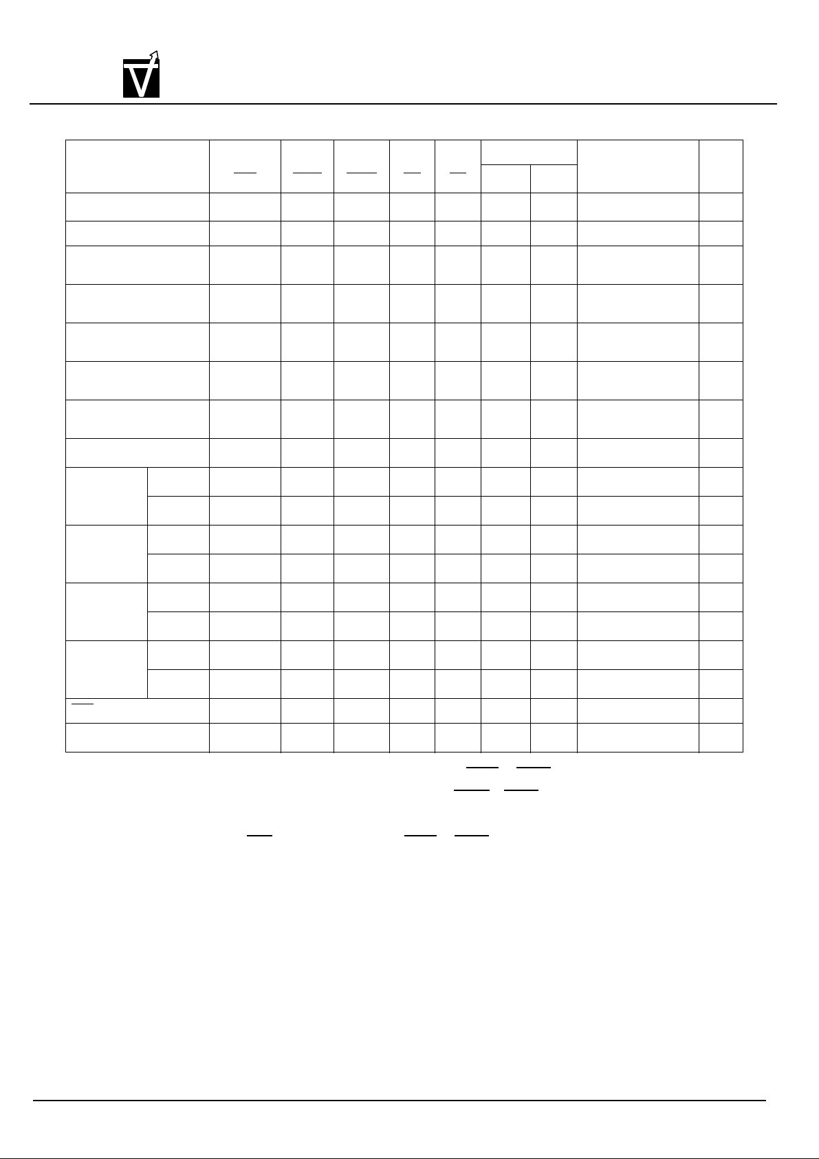
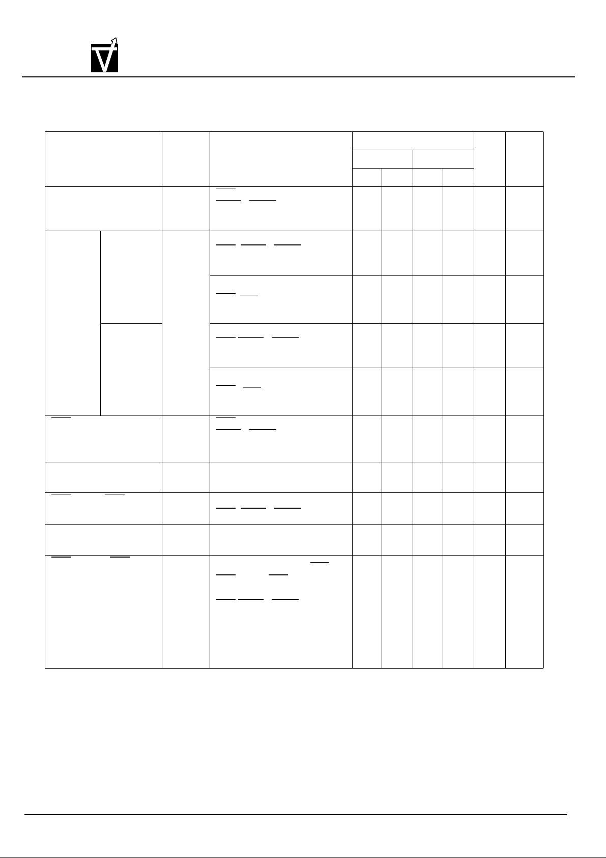
TRUTH TABLE
FUNCTION
VG26(V)(S)18165C
1,048,576 x 16 - Bit
CMOS Dynamic RAM
ADDRESSES
RAS LCAS UCAS WE OE
ROW COL
DQ
S
Notes
STANDBY H
READ : WORD L L L H L ROW COL Data-Out
READ : LOWER BYTE L L H H L ROW COL Lower Byte: Data-Out
READ: UPPER BYTE L H L H L ROW COL Lower Byte: High-Z
WRITE: WORD
(EARLY WRITE)
WRITE: LOWER
BYTE (EARLY)
WRITE : UPPER
BYTE (EARLY)
READ WRITE L L L ROW COL Data-Out, Data-In 1,2
PAGE-MODE
READ
PAGE-MODE
WRITE
PAGE-MODE
READWRITE
1st Cycle L H L ROW COL Data-Out 2
2nd Cycle L H L n/a COL Data-Out 2
1st Cycle L L X ROW COL Data-In 1
2nd Cycle L L X n/a COL Data-In 1
1st Cycle L ROW COL Data-Out, Data-In 1,2
2nd Cycle L n/a COL Data-Out, Data-In 1,2
L L L L X ROW COL Data-In
L L H L X ROW COL Lower Byte: Data-In
L H L L X ROW COL Lower Byte: High-Z
X X X X High-Z
Upper Byte: High-Z
Upper Byte: Data-Out
Upper Byte: High-Z
Upper Byte: Data-In
HIDDEN
REFRESH
RAS-ONLY REFRESH L H H X X ROW n/a High-Z
CBR REFRESH L L H X X X High-Z 4
READ L L H L ROW COL Data-Out 2
WRITE L L L X ROW COL Data-In 1,3
Notes: 1. These WRITE cycles may also be BYTE WRITE cycles (either LCAS or UCAS active).
2. These READ cycles may also be BYTE READ cycles (either LCAS or UCAS active).
3. EARLY WRITE only.
4. At least one of the two CAS signals must be active (LCAS or UCAS).
Document:1G5-0147 Rev.1 Page 4
VG26(V)(S)18165C
1,048,576 x 16 - Bit
VIS
Absolute Maximum Ratings
Voltage on any pin relative to Vss
3.3V
5V
Supply voltage relative to Vss
3.3V
Short circuit output current I
Power dissipation P
Operating temperature T
Storage temperature T
Recommended DC Operating Conditions
Parameter/Condition Symbol 5 Volt Version 3.3 Volt Version Unit
CMOS Dynamic RAM
Parameter Symbol Value Unit
5V
V
V
CC
OUT
OPT
STG
-1.0 to + 7.0
T
D
-0.5 to + 4.6
-1.0 to + 7.0
-0.5 to + 4.6
50 mA
1.0 W
0 to + 70 ¢J
-55 to + 125 ¢J
V
V
Min Typ Max Min Typ Max
Supply Voltage V
Input High Voltage, all inputs V
Input Low Voltage, all inputs V
Capacitance
Ta = 25°C, V
Input capacitance (Address) C
Input capacitance
, LCAS , UCAS, OE, WE)
(RAS
Output capacitance
(Data-in, Data-out)
Note: 1. Capacitance measured with effective capacitance measuring method.
2. RAS
= 5V % or 3.3V %, f = 1MHz
CC
, LCAS and UCAS = V
10± 10±
Parameter Symbol Typ Max Unit Note
CC
IH
IL
to disable Dout.
IH
4.5 5.0 5.5 3.0 3.3 3.6 V
2.4 -V
-1.0 - 0.8 -0.3 - 0.8 V
I1
C
I2
C
I/O
+ 1.0 2.0 -V
CC
- 5 pF 1
- 7 pF 1
- 7 pF 1, 2
+ 0.3 V
CC
Document:1G5-0147 Rev.1 Page 5
VG26(V)(S)18165C
10±
≥
≥
t
100µs≥µA
≤
0VVIL0.2V
≤≤
0.2VV
≤≤
t
300ns
≤
µA
1,048,576 x 16 - Bit
VIS
DC Characteristics; 5- Volt Verion
(T
= 0 to + 70 °C, V
a
Parameter Symbol Test Conditions VG26(V)(S)18165C Unit Notes
CMOS Dynamic RAM
= + 5V %,V
CC
SS
= 0V)
-5 -6
Min Max Min Max
Operating current I
Low
power
S-version
Standby
Current
RAS-only
refresh current
EDO page mode
current
Standard
power
version
CC1
I
CC2
I
CC3
I
CC4
RAS cycling
LCAS / UCAS cycling
t
= min
RC
TTL interface
RAS, LCAS / UCAS = VIH
Dout = High-Z
CMOS interface
RAS,-0.2V
CASVcc
Dout = High-Z
TTL interface
RAS,LCAS / UCAS = VIH
Dout = High-Z
CMOS interface
RAS, -0.2V
CASVcc
Dout = High-Z
RAS cycling,
LCAS / UCAS = VIH
t
= min
RC
t
= min - 90 - 80 mA 1, 3
RC
- 120 - 110 mA 1, 2
- 2 - 2 mA
- 0.25 - 0.25 mA
2 - 2 mA
1 - 1 mA
- 120 - 110 mA 1, 2
CAS-before-RAS
refresh current
Self-refresh current
(S - Version)
CAS- before- RAS long
refresh current
(S-Version)
I
CC5
I
CC8
I
CC9
t
= min
RC
RAS, LCAS / UCAS cycling
RAS
Standby: VCCCAS before RAS refresh:
2048 cycles / 128ms
RAS,LCAS / UCAS:
VCC-(Max)
Dout = High-Z,
0.2VRAS
IHVIH
RAS
- 120 - 110 mA 1, 2
- 350 - 350
- 500 - 500
Document:1G5-0147 Rev.1 Page 6
VG26(V)(S)18165C
10±
VINV
µA
V
µA
1,048,576 x 16 - Bit
VIS
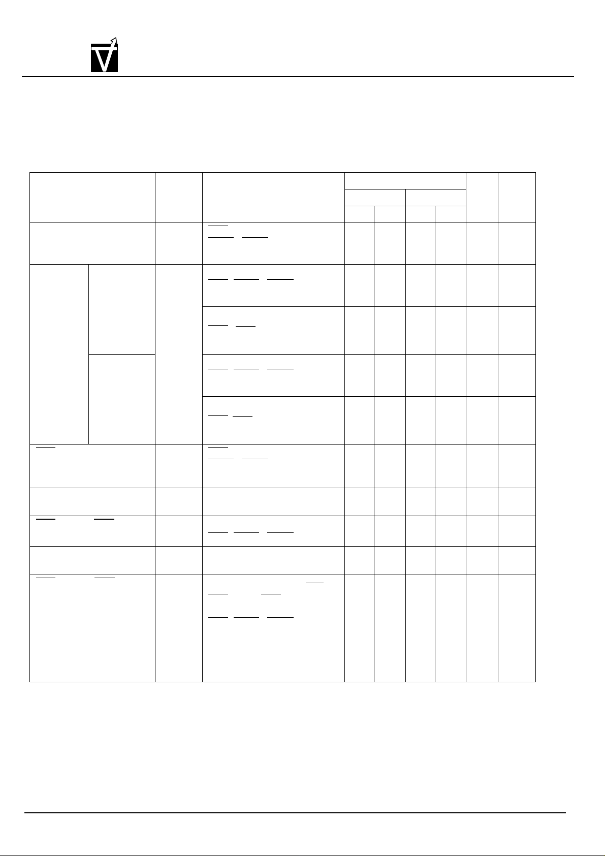
DC Characteristics ; 5-Volt Version (Cont.)
(T
= 0 to + 70°C, V
a
Parameter Symbol Test Conditions
Input leakage current I
Output leakage current I
Output high Voltage V
Output low voltage V
Notes:
1. ICC is specified as an average current. It depends on output loading condition and cycle rate when the
CMOS Dynamic RAM
= + 5V %,V
CC
LI
LO
OH
OL
= 0V)
SS
VG26(V)(S)18165C
-5 -6
Min Max Min Max
0V
≤≤
0V
≤≤
OUTVCC
Dout = Disable
IOH = - 5mA 2.4 - 2.4 - V
IOL = + 4.2mA - 0.4 - 0.4 V
CC
+ 0.5V
+ 0.5V
-5 5 -5 5
-5 5 -5 5
Unit Notes
device is selected. ICC max is specified at the output open condition.
2. Address can be changed once or less while RAS = VIL.
3. For I
, address can be changed once or less within one EDO page mode cycle time.
CC4
Document:1G5-0147 Rev.1 Page 7
VG26(V)(S)18165C
10±
t
100µs≥µA
≤
0VVIL0.2V
≤≤
0.2VV
≤≤
t
300ns
≤
µA
1,048,576 x 16 - Bit
VIS
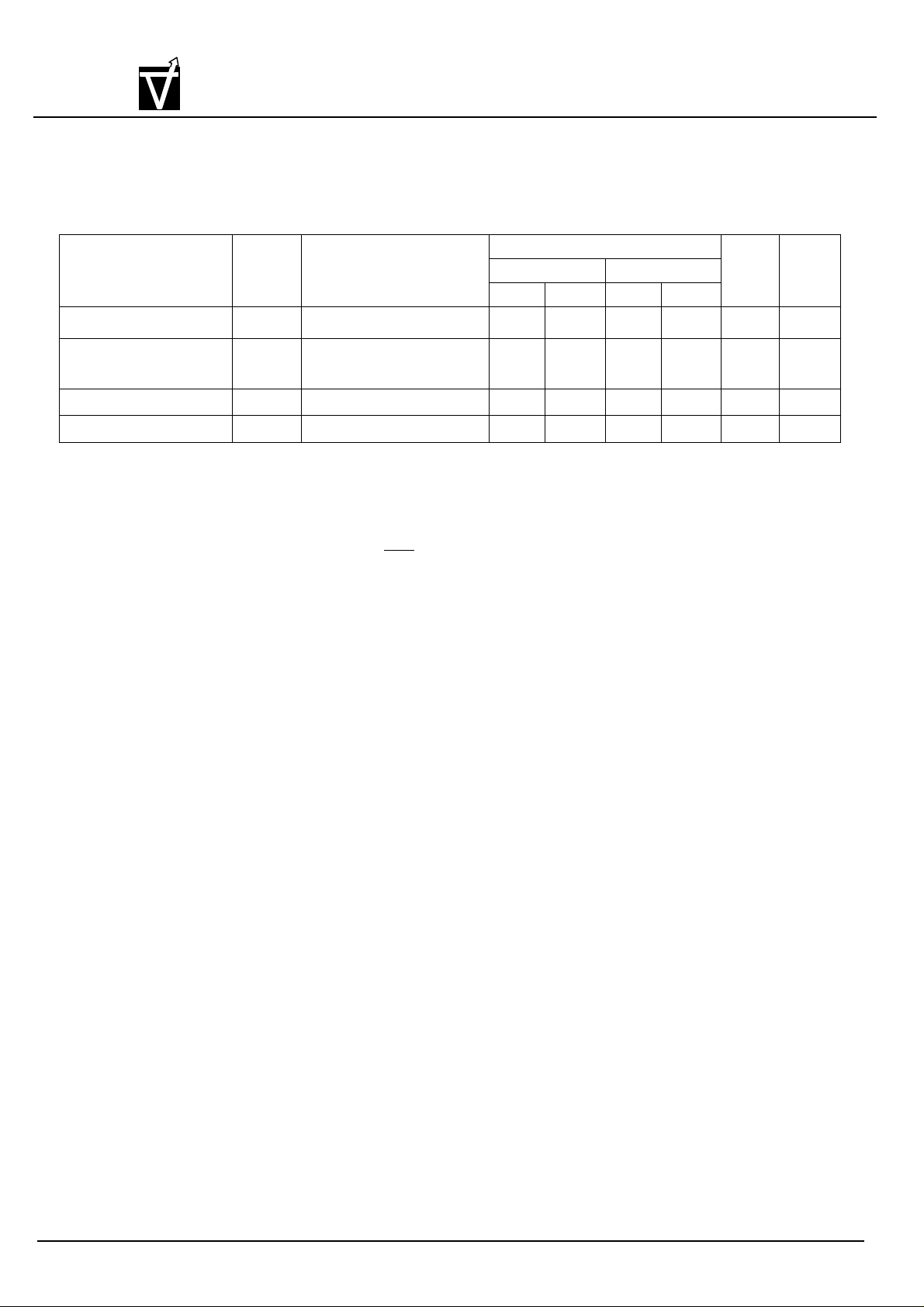
DC Characteristics ; 3.3 - Volt Version
(T
= 0 to 70°C, V
a
Parameter Symbol Test Conditions VG26(V)(S)18165C Unit Notes
Operating current I
Standby
Current
RAS- only refresh current I
EDO page mode current I
CMOS Dynamic RAM
= + 3.3V %, V
CC
CC1
Low
power
S-version
Standard
power
version
I
CC2
CC3
CC4
= 0V)
SS
-5 -6
Min Max Min Max
RAS cycling
LCAS / UCAS cycling
t
= min
RC
LVTTL interface
RAS, LCAS / UCAS = VIH
Dout = High-Z
CMOS interface
RAS, -0.2V
CASVCC≥
Dout = High-Z
LVTTL interface
RAS, LCAS / UCAS = VIH
Dout = High-Z
CMOS interface
RAS,-0.2V
CASVCC≥
Dout = High-Z
RAS cycling
LCAS / UCAS = VIH
t
= min
RC
t
= min - 90 - 80 mA 1, 3
PC
- 120 - 110 mA 1, 2
- 0.5 - 0.5 mA
- 0.15 - 0.15 mA
- 2 - 2 mA
- 0.5 - 0.5 mA
- 120 - 110 mA 1, 2
CAS- before- RAS refresh
current
Self- refresh current
(S-Version)
CAS- before- RAS long
refresh current
(S-Version)
Document:1G5-0147 Rev.1 Page 8
I
CC5
I
CC8
I
CC9
t
= min
RC
RAS, LCAS / UCAS cycling
RASS
Standby: VCCCAS before RAS refresh:
2048 cycles / 128ms
RAS, LCAS / UCAS :
VCC-(max)
Dout = High-Z,
0.2VRAS
IHVIH
RAS
- 120 - 110 mA 1, 2
- 250 - 250
- 300 - 300
VG26(V)(S)18165C
10±
0VVinV
≤≤
µA
0VVoutV
≤≤
µA
1,048,576 x 16 - Bit
VIS
DC Characteristics ; 3.3 - Volt Version (Cont.)
(Ta = 0 to 70°C, V
Parameter Symbol Test Conditions
Input leakage current I
Output leakage current I
Output high Voltage V
Output low voltage V
Notes:
1. ICC is specified as an average current. It depends on output loading condition and cycle rate when the
CMOS Dynamic RAM
= +3.3V %, V
CC
LI
LO
OH
OL
= 0V)
SS
VG26(V)(S)18165C Unit Notes
-5 -6
Min Max Min Max
+ 0.3V
CC
+ 0.3V
CC
Dout = Disable
IOH = -2mA 2.4 - 2.4 - V
IOL = +2mA - 0.4 - 0.4 V
-5 5 -5 5
-5 5 -5 5
device is selected. ICC max is specified at the output open condition.
2. Address can be changed once or less while RAS = VIL.
3. For I
, address can be changed once or less within one EDO page mode cycle time.
CC4
Document:1G5-0147 Rev.1 Page 9
 Loading...