

VIS VG26V17405J-5, VG26S17405J-6, VG26S17405J-5, VG26V17405J-6 Datasheet

VG26(V)(S)17405FJ
10±
4,194,304 x 4 - Bit
VIS
Description
The device CMOS Dynamic RAM organized as 4,194,304 words x 4 bits with extended data out access
mode. It is fabricated with an advanced submicron CMOS technology and designed to operate from a single
5V only or 3.3V oniy power supply. Low voltage operation is more suitable to be used on battery backup,
portable electronic application. A new refresh feature called “self-refresh” is supported and very slow CBR
cycles are being performed. lt is packaged in JEDEC standard 26/24-pin plastic SOJ.
Features
• Single 5V(%) or 3.3V(+10%,-5%) only power supply
CMOS Dynamic RAM
• High speed t
• Low power dissipation
- Active wode : 5V version 660/605 mW (Mas)
3.3V version 432/396 mW (Mas)
- Standby mode: 5V version 1.375 mW (Mas)
3.3V version 0.54 mW (Mas)
• Extended - data - out(EDO) page mode access
• I/O level: TTL compatible (Vcc = 5V)
LVTTL compatible (Vcc = 3.3V)
• 2048 refresh cycle in 32 ms(Std.) or 128 ms(S-version)
• 4 refresh modesh:
- RAS only refresh
- CAS - before - RAS refresh
- Hidden refresh
- Self-refresh(S-version)
acess time: 50/60ns
RAC
Document:1G5-0162 Rev.1 Page 1
VIS
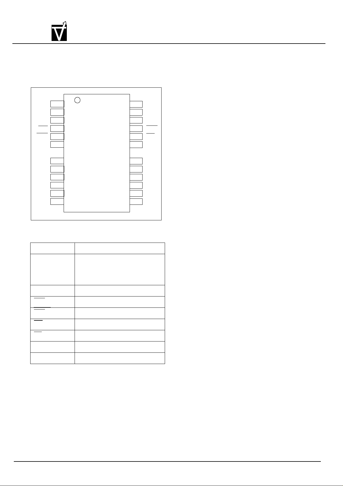
Pin Configuration
26/24-PIN 300mil Plastic SOJ
VG26(V)(S)17405FJ
4,194,304 x 4 - Bit
CMOS Dynamic RAM
VCC
DQ1
DQ2
WE
RAS
NC
A10
A0
A1
A2
A3
VCC
Pin Description
Pin Name Function
A0-A10 Address inputs
1
2
3
4
5
6
8
9
10
11
12
13
VG26(V)(S)17405J
- Row address
- Column address
- Refresh address
26
25
24
23
22
21
19
18
17
16
15
14
VSS
DQ4
DQ3
CAS
OE
A9
A8
A7
A6
A5
A4
VSS
A0-A10
A0-A10
A0-A10
DQ1~DQ4 Data-in / data-out
RAS Row address strobe
CAS Column address strobe
WE Write enable
OE Output enable
Vcc Power (+5 V or + 3.3V)
Vss Ground
Document:1G5-0162 Rev.1 Page 2
VIS
Block Diagram
WE
VG26(V)(S)17405FJ
4,194,304 x 4 - Bit
CMOS Dynamic RAM
A0
A1
A2
A3
A4
A5
A6
A7
A8
A9
A10
CAS
NO. 2 CLOCK
GENERATOR
COLUMN
ADDRESS
BUFFERS (11)
REFRESH
CONTROLLER
REFRESH
COUNTER
ROW
ADDRESS
BUFFERS (11)
CONTROL
LOGIC
DATA-IN BUFFER
DQ1
.
.
DQ4
DATA-OUT
BUFFER
COLUMN
DECODER
2048
SENSE AMPLIFIERS
I/O GATING
2048x4
2048x2048x4
MEMORY
ROW
DECODER
2048
ARRAY
OE
NO. 1 CLOCK
RAS
GENERATOR
Document:1G5-0162 Rev.1 Page 3
Vcc
Vss
VG26(V)(S)17405FJ
HX→
HL→
LH→
HL→
HL→
HL→
HL→
HL→
HL→LH→
HL→
HL→
LH
LHL→→
LHL→→
HL→
4,194,304 x 4 - Bit
VIS
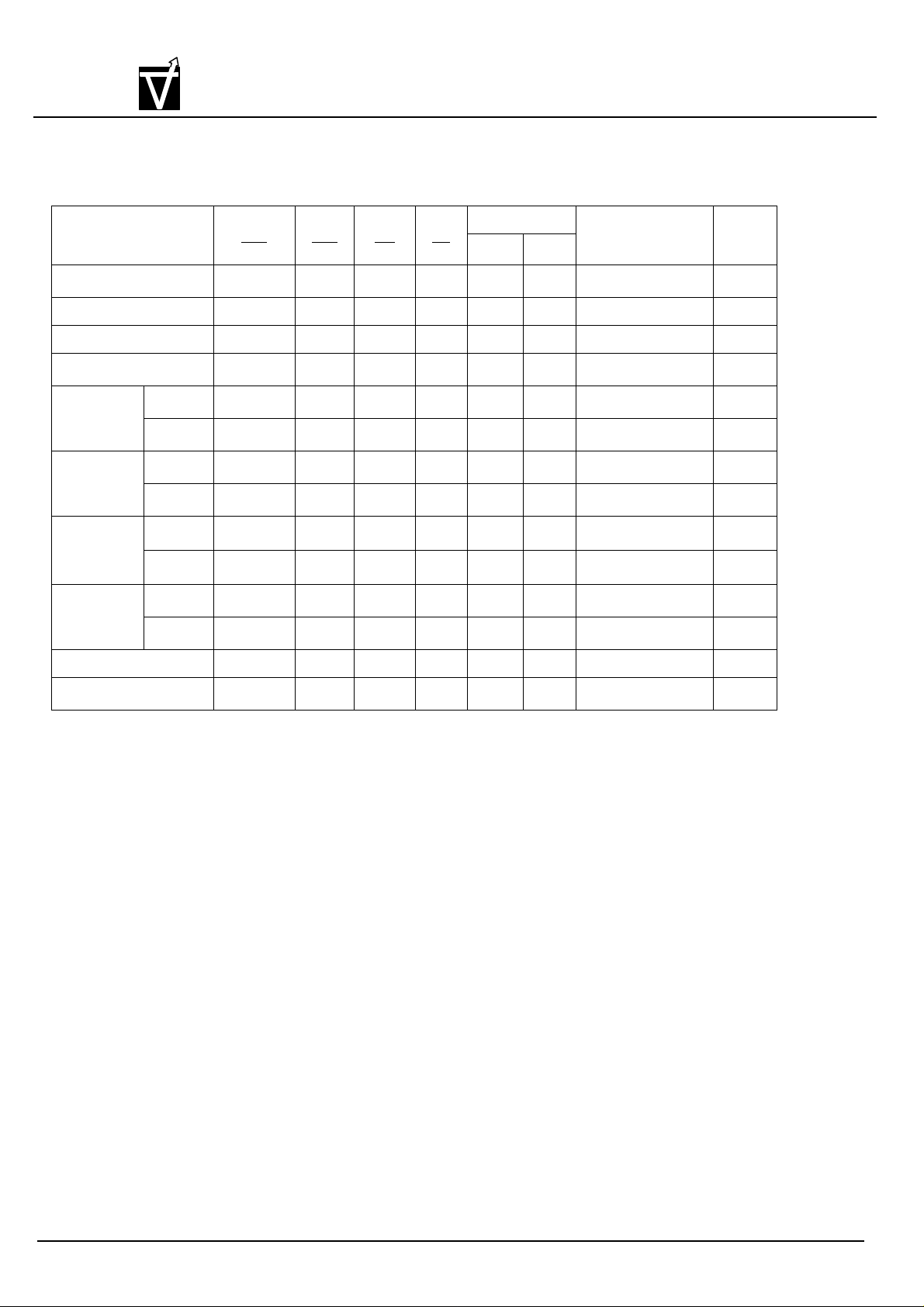
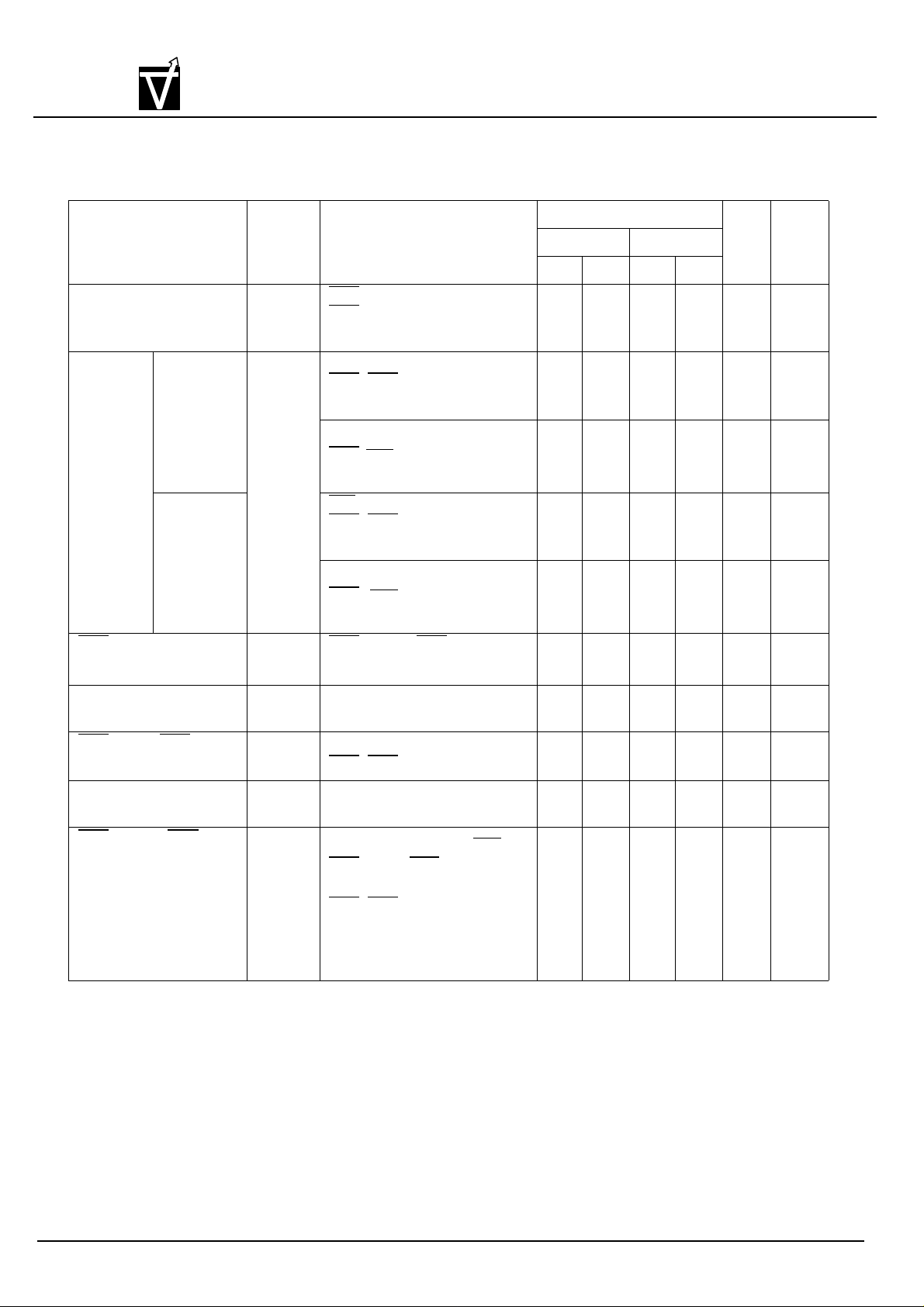
TRUTH TABLE
FUNCTION
STANDBY H X X X X High-Z
READ L L H L ROW COL Data-Out
WRITE: (EARLY WRITE ) L L L X ROW COL Data-ln
READ WRITE L L ROW COL Data-Out,Data-ln
CMOS Dynamic RAM
ADDRESSES
RAS CAS WE OE
ROW COL
DQ
S
Notes
EDO-PAGEMODE READ
EDO-PAGE
MODE WRITE
EDO-
PAGE-MODE
READ-WRITE
HIDDEN
REFRESH
RAS-ONLY REFRESH L H X X ROW n/a High-Z
CBR REFRESH L H X X X High-Z
1st Cycle L H L ROW COL Data-Out
2nd Cycle L H L n/a COL Data-Out
1st Cycle L L X ROW COL Data-In
2nd Cycle L L X n/a COL Data-In
1st Cycle L ROW COL Data-Out, Data-In
2nd Cycle L n/a COL Data-Out, Data-In
READ L H L ROW COL Data-Out
WRITE L L X ROW COL Data-In 1
→
Notes: 1. EARLY WRITE only.
Document:1G5-0162 Rev.1 Page 4
VG26(V)(S)17405FJ
10±
4,194,304 x 4 - Bit
VIS
Absolute Maximum Ratings
Voltage on any pin relative to Vss
3.3V
5V
Supply voltage relative to Vss
3.3V
Short circuit output current I
Power dissipation P
Operating temperature T
Storage temperature T
Recommended DC Operating Conditions
Parameter/Condition Symbol 5 Volt Version 3.3 Volt Version Unit
CMOS Dynamic RAM
Parameter Symbol Value Unit
5V
V
V
OUT
OPT
STG
CC
-1.0 to + 7.0
T
D
-0.5 to + 4.6
-1.0 to + 7.0
-0.5 to + 4.6
50 mA
1.0 W
0 to + 70
-55 to + 125
V
V
°C
°C
Min Typ Max Min Typ Max
Supply Voltage V
Input High Voltage, all inputs V
Input Low Voltage, all inputs V
Capacitance
Ta = 25°C, VCC = 5V % or 3.3V (+10%,-5%), f = 1MHz
Parameter Symbol Typ Max Unit Note
Input capacitance (Address) C
Input capacitance (RAS, CAS, OE, WE) C
Output capacitance
(Data-in, Data-out)
Note: 1. Capacitance measured with effective capacitance measuring method.
2. RAS, CAS = V
to disable Dout.
IH
CC
IH
IL
4.5 5.0 5.5 3.15 3.3 3.6 V
2.4
-1.0
C
I1
I2
I/O
V
-
-
+ 1.0 2.0 - V
CC
0.8 -0.3 - 0.8 V
-
-
-
+ 0.3 V
CC
5 pF 1
7 pF 1
7 pF 1, 2
Document:1G5-0162 Rev.1 Page 5
VG26(V)(S)17405FJ
10±
≥
≥
t
100µs≥µA
≤
0VV
0.2V
≤≤
0.2VV
≤≤
t
300ns
≤
µA
4,194,304 x 4 - Bit
VIS
DC Characteristics; 5- Volt Verion
(T
= 0 to + 70 °C, V
a
Parameter Symbol Test Conditions VG26(V)(S)17405 Unit Notes
CMOS Dynamic RAM
= + 5V ,V
CC
SS
= 0V)
-5 -6
Min Max Min Max
Operating current I
Low
power
S-version
Standby
Current
RAS-only
refresh current
EDO page mode
current
CAS-before-RAS
refresh current
Standard
power
version
CC1
I
CC2
I
CC3
I
CC4
I
CC5
RAS cycling
CAS, cycling
t
= min
RC
TTL interface
RAS, CAS = VIH
Dout = High-Z
CMOS interface
RAS,-0.2V
CASVcc
Dout = High-Z
TTL interface
RAS, CAS = VIH
Dout = High-Z
CMOS interface
RAS, -0.2V
CASVcc
Dout = High-Z
RAS cycling, CAS = VIH
t
= min
RC
t
= min - 90 - 80 mA 1, 3
RC
t
= min
RC
RAS, CAS cycling
- 120 - 110 mA 1, 2
- 2 - 2 mA
- 0.25 - 0.25 mA
2 - 2 mA
1 - 1 mA
- 120 - 110 mA 1, 2
- 120 - 110 mA 1, 2
Self-refresh current
(S - Version)
CAS- before- RAS long
refresh current
(S-Version)
I
CC8
I
CC9
RAS
Standby: VCCCAS before RAS refresh:
2048 cycles / 128ms
RAS, CAS:
VCC-(Max)
Dout = High-Z,
0.2VRAS
IL
IHVIH
RAS
- 350 - 350
- 500 - 500
Document:1G5-0162 Rev.1 Page 6

VG26(V)(S)17405FJ
10±
VINV
µA
V
µA
4,194,304 x 4 - Bit
VIS
DC Characteristics ; 5-Volt Version (Cont.)
(T
= 0 to + 70°C, V
a
Parameter Symbol Test Conditions
Input leakage current I
Output leakage current I
Output high Voltage V
Output low voltage V
Notes:
1. ICC is specified as an average current. It depends on output loading condition and cycle rate when the
CMOS Dynamic RAM
= + 5V %,V
CC
LI
LO
OH
OL
= 0V)
SS
VG26(V)(S) 17405
-5 -6
Min Max Min Max
0V
≤≤
0V
≤≤
OUTVCC
Dout = Disable
IOH = - 5mA 2.4 - 2.4 - V
IOL = + 4.2mA - 0.4 - 0.4 V
CC
+ 0.5V
+ 0.5V
-5 5 -5 5
-5 5 -5 5
Unit Notes
device is selected. ICC max is specified at the output open condition.
2. Address can be changed once or less while RAS = VIL.
3. For I
, address can be changed once or less within one EDO page mode cycle time.
CC4
Document:1G5-0162 Rev.1 Page 7
VG26(V)(S)17405FJ
t
100µs≥µA
≤
0VV
0.2V
≤≤
0.2VV
≤≤
t
300ns
≤
µA
4,194,304 x 4 - Bit
VIS
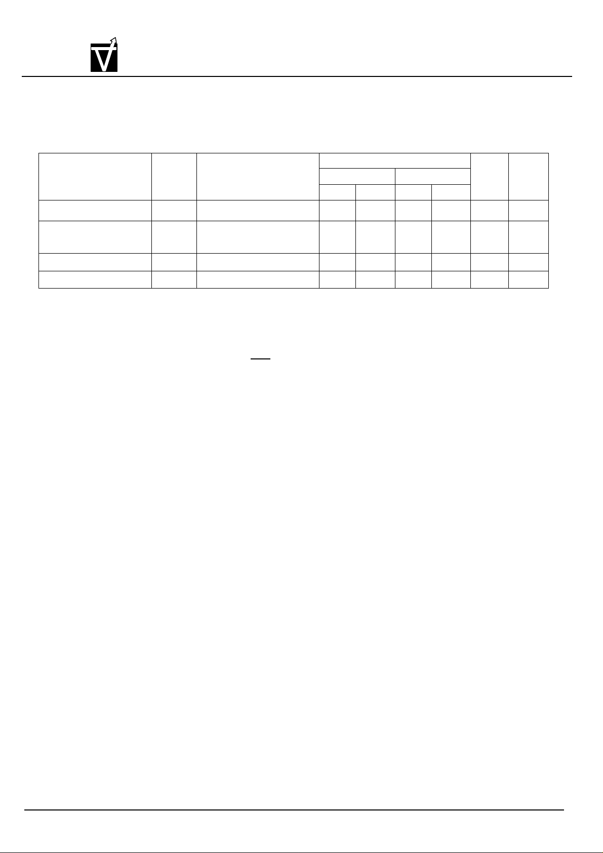
DC Characteristics ; 3.3 - Volt Version
(T
= 0 to 70°C, V
a
Parameter Symbol Test Conditions VG26(V)(S)17405 Unit Notes
Operating current I
Standby
Current
RAS- only refresh current I
EDO page mode current I
CMOS Dynamic RAM
= + 3.3V (+10%,-5%), V
CC
CC1
Low
power
S-version
Standard
power
version
I
CC2
CC3
CC4
= 0V)
SS
-5 -6
Min Max Min Max
RAS cycling
CAS, cycling
t
= min
RC
LVTTL interface
RAS, CAS = VIH
Dout = High-Z
CMOS interface
RAS, -0.2V
CASVCC≥
Dout = High-Z
LVTTL interface
RAS, CAS = VIH
Dout = High-Z
CMOS interface
RAS,-0.2V
CASVCC≥
Dout = High-Z
RAS cycling, CAS = VIH
t
= min
RC
t
= min - 90 - 80 mA 1, 3
PC
- 120 - 110 mA 1, 2
- 0.5 - 0.5 mA
- 0.15 - 0.15 mA
- 2 - 2 mA
- 0.5 - 0.5 mA
- 120 - 110 mA 1, 2
CAS- before- RAS refresh
current
Self- refresh current
(S-Version)
CAS- before- RAS long
refresh current
(S-Version)
I
CC5
I
CC8
I
CC9
t
= min
RC
RAS, CAS cycling
RASS
Standby: VCCCAS before RAS refresh:
2048 cycles / 128ms
RAS, CAS:
VCC-(max)
Dout = High-Z,
0.2VRAS
IL
IHVIH
RAS
- 120 - 110 mA 1, 2
- 250 - 250
- 300 - 300
Document:1G5-0162 Rev.1 Page 8
VG26(V)(S)17405FJ
0VVinV
≤≤
µA
0VVoutV
≤≤
µA
4,194,304 x 4 - Bit
VIS
DC Characteristics ; 3.3 - Volt Version (Cont.)
(Ta = 0 to 70°C, V
Parameter Symbol Test Conditions
Input leakage current I
Output leakage current I
Output high Voltage V
Output low voltage V
Notes:
1. ICC is specified as an average current. It depends on output loading condition and cycle rate when the
CMOS Dynamic RAM
= +3.3V (+10%,-5%), V
CC
LI
LO
OH
OL
Dout = Disable
IOH = -2mA 2.4 - 2.4 - V
IOL = +2mA - 0.4 - 0.4 V
SS
= 0V)
CC
CC
+ 0.3V
+ 0.3V
VG26(V)(S) 17405 Unit Notes
-5 -6
Min Max Min Max
-5 5 -5 5
-5 5 -5 5
device is selected. ICC max is specified at the output open condition.
2. Address can be changed once or less while RAS = VIL.
3. For I
, address can be changed once or less within one EDO page mode cycle time.
CC4
Document:1G5-0162 Rev.1 Page 9
 Loading...