

Page 1

SERVICE MANUAL
VIKING® VX
900 MHz LTR-Net
75W-160W Repeater
Part No. 242-2009-632/634
First Printing
March 1999
®
Part No. 001-2009-600 3-99mwp Printed in U.S.A.
1-1
October 1995
Part No. 001-2008-202
Page 2

October 1995
Part No. 001-2008-202
1-2
Page 3

900 MHz LTR-Net REPEATER
PART NO. 242-2009-632/634
Copyright© 1999 by Transcrypt International, Inc.
VIKING® VX
Transcrypt International, Inc. designs and manufactures two-way radio equipment to serve a wide variety of communications
needs. Transcrypt International Inc. produces EFJohnson
services which include business, industrial, government, public safety, and personal users.
LAND MOBILE PRODUCT WARRANTY
The manufacturer’s warranty statement for this product is available from your produc t supplier or fro m the Transcrypt International, Inc., 299 Johnson Avenue, Box 1249, Waseca, MN 56093-0514. Phone (507) 835-6222.
DO NOT allow the antenna to touch or come in very close proximity with the eyes, face, or any exposed body parts while the
radio is transmitting.
DO NOT operate the transmitter of a mobile radio whena person outside the vehicle is within one (1) meter of the antenna.
DO NOT operate the transmitter of a stationary radio (base station, repeater or marine radio) when a person is within one (1)
meter of the antenna.
®
brand equipment for the mobile telephone and land mobile radio
WARNING
DO NOT operate the radio in explosive or flammable atmospheres. The transmitted radio energy could trigger blasting caps
or cause an explosion.
DO NOT operate the radio without the proper antenna installed.
DO NOT allow children to operate or play with this equipment.
NOTE: The above warning list is not intended to include all hazards that may be encountered when using this radio.
This device complies with Part 15 of the FCC rules. Operation is subject to the condition that this device does not cause harmful interference. In addition, changes or modification to this equipment not expressly approved by Transcrypt International,
Inc. could void the user’s authority to ope rate this equipment (FCC rules, 47CFR Part 15.19).
SAFETY INFORMATION
Proper operation of this radio will result in user exposure below the Occupational Safety and Health Act and Federal Communication Commission lim its.
The information in this document is subject to change without notice.
Transcrypt International Inc. will not be liable for any misunderstanding due to misinformation or errors found in this document.
LTR, Multi-Net, LTR-Net, Viking Head/EFJohnson Logo, Call Guard and SUMMIT are registered trademarks of Transcrypt
International, Inc. All other company and/or product names used in this manual are trademarks and/or registered trademarks
of their respective manufacturer.
1-3
October 1995
Part No. 001-2008-202
Page 4

October 1995
Part No. 001-2008-202
1-4
Page 5

TABLE OF CONTENTS (CONT’D)
1 INTRODUCTION AND OPERATION
1.1 SCOPE OF MANUAL . . . . . . . . . . . . . . . . . . . . . . . . . . . . . . . . . . . . . . . . . . . . . . . . . . . . . . . . . . . . . . . . . . . . . . . 1-1
1.2 REPEATER IDENTIFICATION. . . . . . . . . . . . . . . . . . . . . . . . . . . . . . . . . . . . . . . . . . . . . . . . . . . . . . . . . . . . . . 1-1
1.3 MODEL NUMBER BREAKDOWN . . . . . . . . . . . . . . . . . . . . . . . . . . . . . . . . . . . . . . . . . . . . . . . . . . . . . . . . . . . 1-1
1.4 REPEATER DESCRIPTION . . . . . . . . . . . . . . . . . . . . . . . . . . . . . . . . . . . . . . . . . . . . . . . . . . . . . . . . . . . . . . . . . 1-1
TRUNKED SYSTEM . . . . . . . . . . . . . . . . . . . . . . . . . . . . . . . . . . . . . . . . . . . . . . . . . . . . . . . . . . . . . . . . . . . . . . . . 1-1
LTR-Net TRUNKED SYSTEM. . . . . . . . . . . . . . . . . . . . . . . . . . . . . . . . . . . . . . . . . . . . . . . . . . . . . . . . . . . . . . . . . 1-1
1.5 LTR-Net SIGNALING. . . . . . . . . . . . . . . . . . . . . . . . . . . . . . . . . . . . . . . . . . . . . . . . . . . . . . . . . . . . . . . . . . . . . . . 1-2
1.6 ACCESSORIES . . . . . . . . . . . . . . . . . . . . . . . . . . . . . . . . . . . . . . . . . . . . . . . . . . . . . . . . . . . . . . . . . . . . . . . . . . . . 1-2
1.7 PRODUCT WARRANTY . . . . . . . . . . . . . . . . . . . . . . . . . . . . . . . . . . . . . . . . . . . . . . . . . . . . . . . . . . . . . . . . . . . . 1-3
1.8 FACTORY CUSTOMER SERVICE . . . . . . . . . . . . . . . . . . . . . . . . . . . . . . . . . . . . . . . . . . . . . . . . . . . . . . . . . . . 1-3
1.9 FACTORY RETURNS . . . . . . . . . . . . . . . . . . . . . . . . . . . . . . . . . . . . . . . . . . . . . . . . . . . . . . . . . . . . . . . . . . . . . . 1-4
1.10 REPLACEMENT PARTS. . . . . . . . . . . . . . . . . . . . . . . . . . . . . . . . . . . . . . . . . . . . . . . . . . . . . . . . . . . . . . . . . . . . 1-4
1.11 INTERNET HOME PAGE . . . . . . . . . . . . . . . . . . . . . . . . . . . . . . . . . . . . . . . . . . . . . . . . . . . . . . . . . . . . . . . . . . . 1-4
1.12 SOFTWARE UPDATES/REVISIONS . . . . . . . . . . . . . . . . . . . . . . . . . . . . . . . . . . . . . . . . . . . . . . . . . . . . . . . . . 1-4
1.13 REPEATER OPERATION. . . . . . . . . . . . . . . . . . . . . . . . . . . . . . . . . . . . . . . . . . . . . . . . . . . . . . . . . . . . . . . . . . . 1-5
MAIN PROCESSOR CARD (MPC) . . . . . . . . . . . . . . . . . . . . . . . . . . . . . . . . . . . . . . . . . . . . . . . . . . . . . . . . . . . . . 1-5
TEST MODE . . . . . . . . . . . . . . . . . . . . . . . . . . . . . . . . . . . . . . . . . . . . . . . . . . . . . . . . . . . . . . . . . . . . . . . . . . . . . . . 1-5
MAIN AUDIO CARD (MAC). . . . . . . . . . . . . . . . . . . . . . . . . . . . . . . . . . . . . . . . . . . . . . . . . . . . . . . . . . . . . . . . . . 1-7
INTERFACE ALARM CARD (IAC) . . . . . . . . . . . . . . . . . . . . . . . . . . . . . . . . . . . . . . . . . . . . . . . . . . . . . . . . . . . . 1-7
POWER SUPPLY . . . . . . . . . . . . . . . . . . . . . . . . . . . . . . . . . . . . . . . . . . . . . . . . . . . . . . . . . . . . . . . . . . . . . . . . . . . 1-8
1.14 LTR-Net SYSTEM COMPONENTS . . . . . . . . . . . . . . . . . . . . . . . . . . . . . . . . . . . . . . . . . . . . . . . . . . . . . . . . . . . 1-8
INTRODUCTION . . . . . . . . . . . . . . . . . . . . . . . . . . . . . . . . . . . . . . . . . . . . . . . . . . . . . . . . . . . . . . . . . . . . . . . . . . . 1-8
MOBILE TRANSCEIVERS . . . . . . . . . . . . . . . . . . . . . . . . . . . . . . . . . . . . . . . . . . . . . . . . . . . . . . . . . . . . . . . . . . . 1-8
REPEATERS . . . . . . . . . . . . . . . . . . . . . . . . . . . . . . . . . . . . . . . . . . . . . . . . . . . . . . . . . . . . . . . . . . . . . . . . . . . . . . . 1-8
SWITCH. . . . . . . . . . . . . . . . . . . . . . . . . . . . . . . . . . . . . . . . . . . . . . . . . . . . . . . . . . . . . . . . . . . . . . . . . . . . . . . . . . 1-10
CALL PROCESSOR AND SYSTEM and SUBSCRIBER MANAGER . . . . . . . . . . . . . . . . . . . . . . . . . . . . . . . . 1-10
LOCALITY . . . . . . . . . . . . . . . . . . . . . . . . . . . . . . . . . . . . . . . . . . . . . . . . . . . . . . . . . . . . . . . . . . . . . . . . . . . . . . . 1-10
HOME REPEATER CHANNEL. . . . . . . . . . . . . . . . . . . . . . . . . . . . . . . . . . . . . . . . . . . . . . . . . . . . . . . . . . . . . . . 1-10
STATUS REPEATER CHANNEL . . . . . . . . . . . . . . . . . . . . . . . . . . . . . . . . . . . . . . . . . . . . . . . . . . . . . . . . . . . . . 1-10
MONITOR REPEATER CHANNEL . . . . . . . . . . . . . . . . . . . . . . . . . . . . . . . . . . . . . . . . . . . . . . . . . . . . . . . . . . . 1-10
HOME CHANNEL ALIASING . . . . . . . . . . . . . . . . . . . . . . . . . . . . . . . . . . . . . . . . . . . . . . . . . . . . . . . . . . . . . . . 1-10
TELEPHONE INTERCONNECT AND DATA TRANSMISSION. . . . . . . . . . . . . . . . . . . . . . . . . . . . . . . . . . . . 1-11
PUBLIC SWITCHED TELEPHONE NETWORK (PSTN) . . . . . . . . . . . . . . . . . . . . . . . . . . . . . . . . . . . . . . . . . . 1-11
PRIVATE AUTOMATIC BRANCH EXCHANGE (PABX). . . . . . . . . . . . . . . . . . . . . . . . . . . . . . . . . . . . . . . . . 1-11
PULSE CODE MODULATION (PCM) . . . . . . . . . . . . . . . . . . . . . . . . . . . . . . . . . . . . . . . . . . . . . . . . . . . . . . . . . 1-11
1.15 LTR-Net FEATURES . . . . . . . . . . . . . . . . . . . . . . . . . . . . . . . . . . . . . . . . . . . . . . . . . . . . . . . . . . . . . . . . . . . . . . 1-11
STANDARD AND SPECIAL CALLS. . . . . . . . . . . . . . . . . . . . . . . . . . . . . . . . . . . . . . . . . . . . . . . . . . . . . . . . . . 1-11
UNIQUE ID CODES . . . . . . . . . . . . . . . . . . . . . . . . . . . . . . . . . . . . . . . . . . . . . . . . . . . . . . . . . . . . . . . . . . . . . . . 1-11
GROUP IDENTIFICATION CALLS . . . . . . . . . . . . . . . . . . . . . . . . . . . . . . . . . . . . . . . . . . . . . . . . . . . . . . . . . . . 1-12
ALARM FORWARDING TO SWITCH. . . . . . . . . . . . . . . . . . . . . . . . . . . . . . . . . . . . . . . . . . . . . . . . . . . . . . . . . 1-12
1 INSTALLATION
1.1 INTRODUCTION . . . . . . . . . . . . . . . . . . . . . . . . . . . . . . . . . . . . . . . . . . . . . . . . . . . . . . . . . . . . . . . . . . . . . . . . . . 2-1
SITE PREPARATION AND ANTENNA INSTALLATION. . . . . . . . . . . . . . . . . . . . . . . . . . . . . . . . . . . . . . . . . . 2-1
1.2 ENVIRONMENT . . . . . . . . . . . . . . . . . . . . . . . . . . . . . . . . . . . . . . . . . . . . . . . . . . . . . . . . . . . . . . . . . . . . . . . . . . . 2-1
1.3 VENTILATION . . . . . . . . . . . . . . . . . . . . . . . . . . . . . . . . . . . . . . . . . . . . . . . . . . . . . . . . . . . . . . . . . . . . . . . . . . . . 2-1
1.4 AC POWER . . . . . . . . . . . . . . . . . . . . . . . . . . . . . . . . . . . . . . . . . . . . . . . . . . . . . . . . . . . . . . . . . . . . . . . . . . . . . . . 2-1
1.5 BATTERY BACKUP. . . . . . . . . . . . . . . . . . . . . . . . . . . . . . . . . . . . . . . . . . . . . . . . . . . . . . . . . . . . . . . . . . . . . . . . 2-2
1.6 800W POWER SUPPLY . . . . . . . . . . . . . . . . . . . . . . . . . . . . . . . . . . . . . . . . . . . . . . . . . . . . . . . . . . . . . . . . . . . . . 2-2
AC INPUT REQUIREMENTS . . . . . . . . . . . . . . . . . . . . . . . . . . . . . . . . . . . . . . . . . . . . . . . . . . . . . . . . . . . . . . . . . 2-3
i
Page 6

TABLE OF CONTENTS (CONT’D)
1.7 GROUNDING . . . . . . . . . . . . . . . . . . . . . . . . . . . . . . . . . . . . . . . . . . . . . . . . . . . . . . . . . . . . . . . . . . . . . . . . . . . . . .2-3
PROTECTION GUIDELINES. . . . . . . . . . . . . . . . . . . . . . . . . . . . . . . . . . . . . . . . . . . . . . . . . . . . . . . . . . . . . . . . . 2-4
1.8 UNPACKING AND INSPECTION . . . . . . . . . . . . . . . . . . . . . . . . . . . . . . . . . . . . . . . . . . . . . . . . . . . . . . . . . . . . 2-5
1.9 REPEATER DATA BUS INSTALLATION . . . . . . . . . . . . . . . . . . . . . . . . . . . . . . . . . . . . . . . . . . . . . . . . . . . . .2-6
MPC DATA BUS SWITCH SETTINGS. . . . . . . . . . . . . . . . . . . . . . . . . . . . . . . . . . . . . . . . . . . . . . . . . . . . . . . . . 2-6
MPC DATA BUS JUMPER SETTINGS. . . . . . . . . . . . . . . . . . . . . . . . . . . . . . . . . . . . . . . . . . . . . . . . . . . . . . . . . 2-6
1.10 CONNECTING RECEIVE AND TRANSMIT ANTENNAS. . . . . . . . . . . . . . . . . . . . . . . . . . . . . . . . . . . . . . . . 2-7
1.11 CONNECTING AUDIO/DATA LINK TO SWITCH. . . . . . . . . . . . . . . . . . . . . . . . . . . . . . . . . . . . . . . . . . . . . .2-7
VOICE LINK . . . . . . . . . . . . . . . . . . . . . . . . . . . . . . . . . . . . . . . . . . . . . . . . . . . . . . . . . . . . . . . . . . . . . . . . . . . . . . 2-7
DATA LINK. . . . . . . . . . . . . . . . . . . . . . . . . . . . . . . . . . . . . . . . . . . . . . . . . . . . . . . . . . . . . . . . . . . . . . . . . . . . . . . 2-7
1.12 OCXO DRAWER CONNECTIONS. . . . . . . . . . . . . . . . . . . . . . . . . . . . . . . . . . . . . . . . . . . . . . . . . . . . . . . . . . . . 2-8
VIKING VX CONNECTION. . . . . . . . . . . . . . . . . . . . . . . . . . . . . . . . . . . . . . . . . . . . . . . . . . . . . . . . . . . . . . . . . . 2-8
3 SOFTWARE
3.1 INTRODUCTION. . . . . . . . . . . . . . . . . . . . . . . . . . . . . . . . . . . . . . . . . . . . . . . . . . . . . . . . . . . . . . . . . . . . . . . . . . . 3-1
PROGRAMMING SETUP. . . . . . . . . . . . . . . . . . . . . . . . . . . . . . . . . . . . . . . . . . . . . . . . . . . . . . . . . . . . . . . . . . . . 3-1
MINIMUM COMPUTER REQUIREMENTS. . . . . . . . . . . . . . . . . . . . . . . . . . . . . . . . . . . . . . . . . . . . . . . . . . . . . 3-1
PROGRAMMING CABLES . . . . . . . . . . . . . . . . . . . . . . . . . . . . . . . . . . . . . . . . . . . . . . . . . . . . . . . . . . . . . . . . . . 3-2
EEPROM DATA STORAGE. . . . . . . . . . . . . . . . . . . . . . . . . . . . . . . . . . . . . . . . . . . . . . . . . . . . . . . . . . . . . . . . . . 3-2
GETTING STARTED . . . . . . . . . . . . . . . . . . . . . . . . . . . . . . . . . . . . . . . . . . . . . . . . . . . . . . . . . . . . . . . . . . . . . . . 3-2
LIMITATIONS . . . . . . . . . . . . . . . . . . . . . . . . . . . . . . . . . . . . . . . . . . . . . . . . . . . . . . . . . . . . . . . . . . . . . . . . . . . . . 3-2
3.2 MISCELLANEOUS SOFTWARE INFORMATION. . . . . . . . . . . . . . . . . . . . . . . . . . . . . . . . . . . . . . . . . . . . . . 3-3
MINIMUM FREE MEMORY REQUIRED . . . . . . . . . . . . . . . . . . . . . . . . . . . . . . . . . . . . . . . . . . . . . . . . . . . . . . 3-3
SOFTWARE INSTALLATION. . . . . . . . . . . . . . . . . . . . . . . . . . . . . . . . . . . . . . . . . . . . . . . . . . . . . . . . . . . . . . . . 3-3
STARTING THE PROGRAM. . . . . . . . . . . . . . . . . . . . . . . . . . . . . . . . . . . . . . . . . . . . . . . . . . . . . . . . . . . . . . . . . 3-3
3.3 ALIGNMENT SOFTWARE . . . . . . . . . . . . . . . . . . . . . . . . . . . . . . . . . . . . . . . . . . . . . . . . . . . . . . . . . . . . . . . . . .3-3
3.4 HELP . . . . . . . . . . . . . . . . . . . . . . . . . . . . . . . . . . . . . . . . . . . . . . . . . . . . . . . . . . . . . . . . . . . . . . . . . . . . . . . . . . . . .3-3
4 LTR-Net PROGRAMMER
4.1 MENU DISPLAYS . . . . . . . . . . . . . . . . . . . . . . . . . . . . . . . . . . . . . . . . . . . . . . . . . . . . . . . . . . . . . . . . . . . . . . . . . . 4-1
4.2 FILE MENU . . . . . . . . . . . . . . . . . . . . . . . . . . . . . . . . . . . . . . . . . . . . . . . . . . . . . . . . . . . . . . . . . . . . . . . . . . . . . . . 4-1
NEW . . . . . . . . . . . . . . . . . . . . . . . . . . . . . . . . . . . . . . . . . . . . . . . . . . . . . . . . . . . . . . . . . . . . . . . . . . . . . . . . . . . . . 4-1
OPEN . . . . . . . . . . . . . . . . . . . . . . . . . . . . . . . . . . . . . . . . . . . . . . . . . . . . . . . . . . . . . . . . . . . . . . . . . . . . . . . . . . . . 4-1
SAVE AS . . . . . . . . . . . . . . . . . . . . . . . . . . . . . . . . . . . . . . . . . . . . . . . . . . . . . . . . . . . . . . . . . . . . . . . . . . . . . . . . . 4-1
SAVE . . . . . . . . . . . . . . . . . . . . . . . . . . . . . . . . . . . . . . . . . . . . . . . . . . . . . . . . . . . . . . . . . . . . . . . . . . . . . . . . . . . . 4-1
EXIT . . . . . . . . . . . . . . . . . . . . . . . . . . . . . . . . . . . . . . . . . . . . . . . . . . . . . . . . . . . . . . . . . . . . . . . . . . . . . . . . . . . . . 4-1
4.3 EDIT. . . . . . . . . . . . . . . . . . . . . . . . . . . . . . . . . . . . . . . . . . . . . . . . . . . . . . . . . . . . . . . . . . . . . . . . . . . . . . . . . . . . . . 4-2
LOCALITY INFORMATION . . . . . . . . . . . . . . . . . . . . . . . . . . . . . . . . . . . . . . . . . . . . . . . . . . . . . . . . . . . . . . . . . 4-2
SELECT REPEATER. . . . . . . . . . . . . . . . . . . . . . . . . . . . . . . . . . . . . . . . . . . . . . . . . . . . . . . . . . . . . . . . . . . . . . . . 4-3
REPEATER INFORMATION . . . . . . . . . . . . . . . . . . . . . . . . . . . . . . . . . . . . . . . . . . . . . . . . . . . . . . . . . . . . . . . . . 4-4
DELETE REPEATER . . . . . . . . . . . . . . . . . . . . . . . . . . . . . . . . . . . . . . . . . . . . . . . . . . . . . . . . . . . . . . . . . . . . . . . 4-7
4.4 TRANSFER. . . . . . . . . . . . . . . . . . . . . . . . . . . . . . . . . . . . . . . . . . . . . . . . . . . . . . . . . . . . . . . . . . . . . . . . . . . . . . . . 4-7
READ SETUP PARAMETERS. . . . . . . . . . . . . . . . . . . . . . . . . . . . . . . . . . . . . . . . . . . . . . . . . . . . . . . . . . . . . . . . 4-7
WRITE SETUP PARAMETERS. . . . . . . . . . . . . . . . . . . . . . . . . . . . . . . . . . . . . . . . . . . . . . . . . . . . . . . . . . . . . . . 4-7
4.5 HARDWARE . . . . . . . . . . . . . . . . . . . . . . . . . . . . . . . . . . . . . . . . . . . . . . . . . . . . . . . . . . . . . . . . . . . . . . . . . . . . . . 4-8
HSDB MONITOR . . . . . . . . . . . . . . . . . . . . . . . . . . . . . . . . . . . . . . . . . . . . . . . . . . . . . . . . . . . . . . . . . . . . . . . . . . 4-8
RECEIVE/TRANSMIT DATA . . . . . . . . . . . . . . . . . . . . . . . . . . . . . . . . . . . . . . . . . . . . . . . . . . . . . . . . . . . . . . . . 4-8
RF DATA . . . . . . . . . . . . . . . . . . . . . . . . . . . . . . . . . . . . . . . . . . . . . . . . . . . . . . . . . . . . . . . . . . . . . . . . . . . . . . . . . 4-9
INPUT MONITOR. . . . . . . . . . . . . . . . . . . . . . . . . . . . . . . . . . . . . . . . . . . . . . . . . . . . . . . . . . . . . . . . . . . . . . . . . . 4-9
REVISIONS . . . . . . . . . . . . . . . . . . . . . . . . . . . . . . . . . . . . . . . . . . . . . . . . . . . . . . . . . . . . . . . . . . . . . . . . . . . . . . . 4-9
MODE SELECT. . . . . . . . . . . . . . . . . . . . . . . . . . . . . . . . . . . . . . . . . . . . . . . . . . . . . . . . . . . . . . . . . . . . . . . . . . . 4-10
ii
Page 7

TABLE OF CONTENTS (CONT’D)
4.6 TEST . . . . . . . . . . . . . . . . . . . . . . . . . . . . . . . . . . . . . . . . . . . . . . . . . . . . . . . . . . . . . . . . . . . . . . . . . . . . . . . . . . . . 4-10
EXCITER . . . . . . . . . . . . . . . . . . . . . . . . . . . . . . . . . . . . . . . . . . . . . . . . . . . . . . . . . . . . . . . . . . . . . . . . . . . . . . . . . 4-11
POWER AMPLIFIER . . . . . . . . . . . . . . . . . . . . . . . . . . . . . . . . . . . . . . . . . . . . . . . . . . . . . . . . . . . . . . . . . . . . . . . 4-11
RECEIVER. . . . . . . . . . . . . . . . . . . . . . . . . . . . . . . . . . . . . . . . . . . . . . . . . . . . . . . . . . . . . . . . . . . . . . . . . . . . . . . . 4-11
FULL REPEATER. . . . . . . . . . . . . . . . . . . . . . . . . . . . . . . . . . . . . . . . . . . . . . . . . . . . . . . . . . . . . . . . . . . . . . . . . . 4-11
4.7 UTILITIES . . . . . . . . . . . . . . . . . . . . . . . . . . . . . . . . . . . . . . . . . . . . . . . . . . . . . . . . . . . . . . . . . . . . . . . . . . . . . . . 4-11
COM PORT SETUP. . . . . . . . . . . . . . . . . . . . . . . . . . . . . . . . . . . . . . . . . . . . . . . . . . . . . . . . . . . . . . . . . . . . . . . . . 4-11
ALARM DISPLAY . . . . . . . . . . . . . . . . . . . . . . . . . . . . . . . . . . . . . . . . . . . . . . . . . . . . . . . . . . . . . . . . . . . . . . . . . 4-11
4.8 VIEW. . . . . . . . . . . . . . . . . . . . . . . . . . . . . . . . . . . . . . . . . . . . . . . . . . . . . . . . . . . . . . . . . . . . . . . . . . . . . . . . . . . . 4-12
STATUS BAR . . . . . . . . . . . . . . . . . . . . . . . . . . . . . . . . . . . . . . . . . . . . . . . . . . . . . . . . . . . . . . . . . . . . . . . . . . . . . 4-12
TOOLBAR . . . . . . . . . . . . . . . . . . . . . . . . . . . . . . . . . . . . . . . . . . . . . . . . . . . . . . . . . . . . . . . . . . . . . . . . . . . . . . . . 4-12
SAVE SETTINGS ON EXIT. . . . . . . . . . . . . . . . . . . . . . . . . . . . . . . . . . . . . . . . . . . . . . . . . . . . . . . . . . . . . . . . . . 4-12
4.9 HELP . . . . . . . . . . . . . . . . . . . . . . . . . . . . . . . . . . . . . . . . . . . . . . . . . . . . . . . . . . . . . . . . . . . . . . . . . . . . . . . . . . . . 4-12
HELP TOPICS . . . . . . . . . . . . . . . . . . . . . . . . . . . . . . . . . . . . . . . . . . . . . . . . . . . . . . . . . . . . . . . . . . . . . . . . . . . . . 4-12
HELP ON HELP . . . . . . . . . . . . . . . . . . . . . . . . . . . . . . . . . . . . . . . . . . . . . . . . . . . . . . . . . . . . . . . . . . . . . . . . . . . 4-12
ABOUT LTR-Net. . . . . . . . . . . . . . . . . . . . . . . . . . . . . . . . . . . . . . . . . . . . . . . . . . . . . . . . . . . . . . . . . . . . . . . . . . . 4-12
5 REPEATER PROGRAMMING
5.1 OVERVIEW . . . . . . . . . . . . . . . . . . . . . . . . . . . . . . . . . . . . . . . . . . . . . . . . . . . . . . . . . . . . . . . . . . . . . . . . . . . . . . . 5-1
GETTING STARTED . . . . . . . . . . . . . . . . . . . . . . . . . . . . . . . . . . . . . . . . . . . . . . . . . . . . . . . . . . . . . . . . . . . . . . . . 5-1
STARTING THE PROGRAM. . . . . . . . . . . . . . . . . . . . . . . . . . . . . . . . . . . . . . . . . . . . . . . . . . . . . . . . . . . . . . . . . . 5-1
USING THE TOOLBAR . . . . . . . . . . . . . . . . . . . . . . . . . . . . . . . . . . . . . . . . . . . . . . . . . . . . . . . . . . . . . . . . . . . . . . 5-1
LIMITATIONS . . . . . . . . . . . . . . . . . . . . . . . . . . . . . . . . . . . . . . . . . . . . . . . . . . . . . . . . . . . . . . . . . . . . . . . . . . . . . 5-1
5.2 LOCALITY SETUP. . . . . . . . . . . . . . . . . . . . . . . . . . . . . . . . . . . . . . . . . . . . . . . . . . . . . . . . . . . . . . . . . . . . . . . . . 5-1
General Parameters. . . . . . . . . . . . . . . . . . . . . . . . . . . . . . . . . . . . . . . . . . . . . . . . . . . . . . . . . . . . . . . . . . . . . . . . . . . 5-2
5.3 HOW DO I . . . . . . . . . . . . . . . . . . . . . . . . . . . . . . . . . . . . . . . . . . . . . . . . . . . . . . . . . . . . . . . . . . . . . . . . . . . . . . . . 5-2
CREATING A NEW SITE FILE. . . . . . . . . . . . . . . . . . . . . . . . . . . . . . . . . . . . . . . . . . . . . . . . . . . . . . . . . . . . . . . . 5-2
OPEN AN EXISTING SITE FILE. . . . . . . . . . . . . . . . . . . . . . . . . . . . . . . . . . . . . . . . . . . . . . . . . . . . . . . . . . . . . . . 5-2
MODIFY AN EXIXTING SITE FILE. . . . . . . . . . . . . . . . . . . . . . . . . . . . . . . . . . . . . . . . . . . . . . . . . . . . . . . . . . . . 5-2
ADD A REPEATER . . . . . . . . . . . . . . . . . . . . . . . . . . . . . . . . . . . . . . . . . . . . . . . . . . . . . . . . . . . . . . . . . . . . . . . . . 5-2
CHANGE A REPEATER NUMBER . . . . . . . . . . . . . . . . . . . . . . . . . . . . . . . . . . . . . . . . . . . . . . . . . . . . . . . . . . . . 5-2
6 CIRCUIT DESCRIPTION
6.1 RECEIVER . . . . . . . . . . . . . . . . . . . . . . . . . . . . . . . . . . . . . . . . . . . . . . . . . . . . . . . . . . . . . . . . . . . . . . . . . . . . . . . . 6-1
INTRODUCTION . . . . . . . . . . . . . . . . . . . . . . . . . . . . . . . . . . . . . . . . . . . . . . . . . . . . . . . . . . . . . . . . . . . . . . . . . . . 6-1
REGULATED VOLTAGE SUPPLIES. . . . . . . . . . . . . . . . . . . . . . . . . . . . . . . . . . . . . . . . . . . . . . . . . . . . . . . . . . . 6-1
HELICAL FILTER, RF AMPLIFIER . . . . . . . . . . . . . . . . . . . . . . . . . . . . . . . . . . . . . . . . . . . . . . . . . . . . . . . . . . . . 6-1
FIRST MIXER, CRYSTAL FILTER. . . . . . . . . . . . . . . . . . . . . . . . . . . . . . . . . . . . . . . . . . . . . . . . . . . . . . . . . . . . . 6-1
IF AMPLIFIER, CRYSTAL FILTER . . . . . . . . . . . . . . . . . . . . . . . . . . . . . . . . . . . . . . . . . . . . . . . . . . . . . . . . . . . . 6-1
SECOND MIXER/DETECTOR . . . . . . . . . . . . . . . . . . . . . . . . . . . . . . . . . . . . . . . . . . . . . . . . . . . . . . . . . . . . . . . . 6-2
WIDEBAND AUDIO AMPLIFIER . . . . . . . . . . . . . . . . . . . . . . . . . . . . . . . . . . . . . . . . . . . . . . . . . . . . . . . . . . . . . 6-3
RSSI AMPLIFIER . . . . . . . . . . . . . . . . . . . . . . . . . . . . . . . . . . . . . . . . . . . . . . . . . . . . . . . . . . . . . . . . . . . . . . . . . . . 6-3
HIGH STABILITY SYNTHESIZER. . . . . . . . . . . . . . . . . . . . . . . . . . . . . . . . . . . . . . . . . . . . . . . . . . . . . . . . . . . . . 6-3
LOCK DETECT. . . . . . . . . . . . . . . . . . . . . . . . . . . . . . . . . . . . . . . . . . . . . . . . . . . . . . . . . . . . . . . . . . . . . . . . . . . . . 6-5
BUFFER AMPLIFIER. . . . . . . . . . . . . . . . . . . . . . . . . . . . . . . . . . . . . . . . . . . . . . . . . . . . . . . . . . . . . . . . . . . . . . . . 6-5
VCO (A006). . . . . . . . . . . . . . . . . . . . . . . . . . . . . . . . . . . . . . . . . . . . . . . . . . . . . . . . . . . . . . . . . . . . . . . . . . . . . . . . 6-5
ACTIVE FILTER. . . . . . . . . . . . . . . . . . . . . . . . . . . . . . . . . . . . . . . . . . . . . . . . . . . . . . . . . . . . . . . . . . . . . . . . . . . . 6-5
BUFFER. . . . . . . . . . . . . . . . . . . . . . . . . . . . . . . . . . . . . . . . . . . . . . . . . . . . . . . . . . . . . . . . . . . . . . . . . . . . . . . . . . . 6-5
SYNTHESIZER . . . . . . . . . . . . . . . . . . . . . . . . . . . . . . . . . . . . . . . . . . . . . . . . . . . . . . . . . . . . . . . . . . . . . . . . . . . . . 6-6
BUFFER AMPLIFIER. . . . . . . . . . . . . . . . . . . . . . . . . . . . . . . . . . . . . . . . . . . . . . . . . . . . . . . . . . . . . . . . . . . . . . . . 6-7
iii
Page 8

TABLE OF CONTENTS (CONT’D)
LOCK DETECT . . . . . . . . . . . . . . . . . . . . . . . . . . . . . . . . . . . . . . . . . . . . . . . . . . . . . . . . . . . . . . . . . . . . . . . . . . . . 6-7
BUFFER AMPLIFIER . . . . . . . . . . . . . . . . . . . . . . . . . . . . . . . . . . . . . . . . . . . . . . . . . . . . . . . . . . . . . . . . . . . . . . . 6-7
RF AMPLIFIERS . . . . . . . . . . . . . . . . . . . . . . . . . . . . . . . . . . . . . . . . . . . . . . . . . . . . . . . . . . . . . . . . . . . . . . . . . . . 6-7
6.2 EXCITER . . . . . . . . . . . . . . . . . . . . . . . . . . . . . . . . . . . . . . . . . . . . . . . . . . . . . . . . . . . . . . . . . . . . . . . . . . . . . . . . . 6-7
VCO (A007) . . . . . . . . . . . . . . . . . . . . . . . . . . . . . . . . . . . . . . . . . . . . . . . . . . . . . . . . . . . . . . . . . . . . . . . . . . . . . . . 6-7
EXCITER VCO AND TCXO FREQUENCY MODULATION . . . . . . . . . . . . . . . . . . . . . . . . . . . . . . . . . . . . . . . 6-8
ACTIVE FILTER . . . . . . . . . . . . . . . . . . . . . . . . . . . . . . . . . . . . . . . . . . . . . . . . . . . . . . . . . . . . . . . . . . . . . . . . . . . 6-8
BUFFER . . . . . . . . . . . . . . . . . . . . . . . . . . . . . . . . . . . . . . . . . . . . . . . . . . . . . . . . . . . . . . . . . . . . . . . . . . . . . . . . . . 6-8
HIGH STABILITY SYNTHESIZER. . . . . . . . . . . . . . . . . . . . . . . . . . . . . . . . . . . . . . . . . . . . . . . . . . . . . . . . . . . . 6-8
LOCK DETECT . . . . . . . . . . . . . . . . . . . . . . . . . . . . . . . . . . . . . . . . . . . . . . . . . . . . . . . . . . . . . . . . . . . . . . . . . . . . 6-9
BUFFER AMPLIFIER . . . . . . . . . . . . . . . . . . . . . . . . . . . . . . . . . . . . . . . . . . . . . . . . . . . . . . . . . . . . . . . . . . . . . . 6-10
EXCITER SYNTHESIZER . . . . . . . . . . . . . . . . . . . . . . . . . . . . . . . . . . . . . . . . . . . . . . . . . . . . . . . . . . . . . . . . . . 6-10
BUFFER AMPLIFIER . . . . . . . . . . . . . . . . . . . . . . . . . . . . . . . . . . . . . . . . . . . . . . . . . . . . . . . . . . . . . . . . . . . . . . 6-11
BUFFER AMPLIFIER . . . . . . . . . . . . . . . . . . . . . . . . . . . . . . . . . . . . . . . . . . . . . . . . . . . . . . . . . . . . . . . . . . . . . . 6-12
LOCK DETECT . . . . . . . . . . . . . . . . . . . . . . . . . . . . . . . . . . . . . . . . . . . . . . . . . . . . . . . . . . . . . . . . . . . . . . . . . . . 6-12
BUFFER AMPLIFIER . . . . . . . . . . . . . . . . . . . . . . . . . . . . . . . . . . . . . . . . . . . . . . . . . . . . . . . . . . . . . . . . . . . . . . 6-12
RF AMPLIFIERS . . . . . . . . . . . . . . . . . . . . . . . . . . . . . . . . . . . . . . . . . . . . . . . . . . . . . . . . . . . . . . . . . . . . . . . . . . 6-12
6.3 OCXO DRAWER . . . . . . . . . . . . . . . . . . . . . . . . . . . . . . . . . . . . . . . . . . . . . . . . . . . . . . . . . . . . . . . . . . . . . . . . . . 6-12
INTRODUCTION . . . . . . . . . . . . . . . . . . . . . . . . . . . . . . . . . . . . . . . . . . . . . . . . . . . . . . . . . . . . . . . . . . . . . . . . . 6-12
OCXOs, BUFFERS, DIVIDER AND LINE DRIVER . . . . . . . . . . . . . . . . . . . . . . . . . . . . . . . . . . . . . . . . . . . . . 6-14
OCXO SWITCHING . . . . . . . . . . . . . . . . . . . . . . . . . . . . . . . . . . . . . . . . . . . . . . . . . . . . . . . . . . . . . . . . . . . . . . . 6-14
OCXO PULSE DETECTION. . . . . . . . . . . . . . . . . . . . . . . . . . . . . . . . . . . . . . . . . . . . . . . . . . . . . . . . . . . . . . . . . 6-15
DELTA F DETECTION. . . . . . . . . . . . . . . . . . . . . . . . . . . . . . . . . . . . . . . . . . . . . . . . . . . . . . . . . . . . . . . . . . . . . 6-15
6.4 75W POWER AMPLIFIER. . . . . . . . . . . . . . . . . . . . . . . . . . . . . . . . . . . . . . . . . . . . . . . . . . . . . . . . . . . . . . . . . . 6-16
AMPLIFIER/PRE-DRIVER. . . . . . . . . . . . . . . . . . . . . . . . . . . . . . . . . . . . . . . . . . . . . . . . . . . . . . . . . . . . . . . . . . 6-16
DRIVER . . . . . . . . . . . . . . . . . . . . . . . . . . . . . . . . . . . . . . . . . . . . . . . . . . . . . . . . . . . . . . . . . . . . . . . . . . . . . . . . . 6-16
FINAL AMPLIFIERS . . . . . . . . . . . . . . . . . . . . . . . . . . . . . . . . . . . . . . . . . . . . . . . . . . . . . . . . . . . . . . . . . . . . . . 6-16
POWER DETECTORS . . . . . . . . . . . . . . . . . . . . . . . . . . . . . . . . . . . . . . . . . . . . . . . . . . . . . . . . . . . . . . . . . . . . . 6-17
THERMAL SENSOR. . . . . . . . . . . . . . . . . . . . . . . . . . . . . . . . . . . . . . . . . . . . . . . . . . . . . . . . . . . . . . . . . . . . . . . 6-17
FORWARD/REVERSE POWER DETECT, CIRCULATOR, LOW-PASS FILTER . . . . . . . . . . . . . . . . . . . . . 6-17
6.5 160W POWER AMPLIFIER. . . . . . . . . . . . . . . . . . . . . . . . . . . . . . . . . . . . . . . . . . . . . . . . . . . . . . . . . . . . . . . . .6-17
GAIN BLOCK . . . . . . . . . . . . . . . . . . . . . . . . . . . . . . . . . . . . . . . . . . . . . . . . . . . . . . . . . . . . . . . . . . . . . . . . . . . . 6-17
DRIVER . . . . . . . . . . . . . . . . . . . . . . . . . . . . . . . . . . . . . . . . . . . . . . . . . . . . . . . . . . . . . . . . . . . . . . . . . . . . . . . . . 6-17
FINAL AMPLIFIERS . . . . . . . . . . . . . . . . . . . . . . . . . . . . . . . . . . . . . . . . . . . . . . . . . . . . . . . . . . . . . . . . . . . . . . 6-18
POWER DETECTORS . . . . . . . . . . . . . . . . . . . . . . . . . . . . . . . . . . . . . . . . . . . . . . . . . . . . . . . . . . . . . . . . . . . . . 6-18
FORWARD/REVERSE POWER DETECT, CIRCULATOR, LOW-PASS FILTER . . . . . . . . . . . . . . . . . . . . . 6-18
6.6 RF INTERFACE BOARD . . . . . . . . . . . . . . . . . . . . . . . . . . . . . . . . . . . . . . . . . . . . . . . . . . . . . . . . . . . . . . . . . . . 6-19
POWER CONNECTOR. . . . . . . . . . . . . . . . . . . . . . . . . . . . . . . . . . . . . . . . . . . . . . . . . . . . . . . . . . . . . . . . . . . . . 6-19
SIGNAL CONNECTOR (J101) . . . . . . . . . . . . . . . . . . . . . . . . . . . . . . . . . . . . . . . . . . . . . . . . . . . . . . . . . . . . . . . 6-19
FAN CONNECTOR (J104) . . . . . . . . . . . . . . . . . . . . . . . . . . . . . . . . . . . . . . . . . . . . . . . . . . . . . . . . . . . . . . . . . . 6-21
POWER AMPLIFIER CONNECTIONS. . . . . . . . . . . . . . . . . . . . . . . . . . . . . . . . . . . . . . . . . . . . . . . . . . . . . . . . 6-21
EXCITER CONNECTOR (J102). . . . . . . . . . . . . . . . . . . . . . . . . . . . . . . . . . . . . . . . . . . . . . . . . . . . . . . . . . . . . . 6-22
RECEIVER CONNECTOR (J103) . . . . . . . . . . . . . . . . . . . . . . . . . . . . . . . . . . . . . . . . . . . . . . . . . . . . . . . . . . . . 6-23
6.7 800W POWER SUPPLY . . . . . . . . . . . . . . . . . . . . . . . . . . . . . . . . . . . . . . . . . . . . . . . . . . . . . . . . . . . . . . . . . . . . 6-26
FILTER BOARD . . . . . . . . . . . . . . . . . . . . . . . . . . . . . . . . . . . . . . . . . . . . . . . . . . . . . . . . . . . . . . . . . . . . . . . . . . 6-26
POWER FACTOR CORRECTION. . . . . . . . . . . . . . . . . . . . . . . . . . . . . . . . . . . . . . . . . . . . . . . . . . . . . . . . . . . . 6-26
MAIN PULSE WIDTH MODULATOR . . . . . . . . . . . . . . . . . . . . . . . . . . . . . . . . . . . . . . . . . . . . . . . . . . . . . . . . 6-26
SYNCHRONIZING CIRCUITS . . . . . . . . . . . . . . . . . . . . . . . . . . . . . . . . . . . . . . . . . . . . . . . . . . . . . . . . . . . . . . 6-28
FAN AND THERMAL SHUTDOWN. . . . . . . . . . . . . . . . . . . . . . . . . . . . . . . . . . . . . . . . . . . . . . . . . . . . . . . . . . 6-28
+15V CONVERTER . . . . . . . . . . . . . . . . . . . . . . . . . . . . . . . . . . . . . . . . . . . . . . . . . . . . . . . . . . . . . . . . . . . . . . . 6-29
+5V CONVERTER . . . . . . . . . . . . . . . . . . . . . . . . . . . . . . . . . . . . . . . . . . . . . . . . . . . . . . . . . . . . . . . . . . . . . . . . 6-29
-5V CONVERTER . . . . . . . . . . . . . . . . . . . . . . . . . . . . . . . . . . . . . . . . . . . . . . . . . . . . . . . . . . . . . . . . . . . . . . . . . 6-29
POWER SUPPLY REPAIR AND ALIGNMENT. . . . . . . . . . . . . . . . . . . . . . . . . . . . . . . . . . . . . . . . . . . . . . . . . 6-29
iv
Page 9

TABLE OF CONTENTS (CONT’D)
6.8 BATTERY BACK-UP MODULE. . . . . . . . . . . . . . . . . . . . . . . . . . . . . . . . . . . . . . . . . . . . . . . . . . . . . . . . . . . . . 6-30
OPERATION . . . . . . . . . . . . . . . . . . . . . . . . . . . . . . . . . . . . . . . . . . . . . . . . . . . . . . . . . . . . . . . . . . . . . . . . . . . . . . 6-30
CHARGER. . . . . . . . . . . . . . . . . . . . . . . . . . . . . . . . . . . . . . . . . . . . . . . . . . . . . . . . . . . . . . . . . . . . . . . . . . . . . . . . 6-30
REVERSE BATTERY PROTECTION. . . . . . . . . . . . . . . . . . . . . . . . . . . . . . . . . . . . . . . . . . . . . . . . . . . . . . . . . . 6-31
ENGAGING THE RELAY . . . . . . . . . . . . . . . . . . . . . . . . . . . . . . . . . . . . . . . . . . . . . . . . . . . . . . . . . . . . . . . . . . . 6-31
OVER/UNDERVOLTAGE SHUTDOWN . . . . . . . . . . . . . . . . . . . . . . . . . . . . . . . . . . . . . . . . . . . . . . . . . . . . . . . 6-31
BBM FAN CONTROL . . . . . . . . . . . . . . . . . . . . . . . . . . . . . . . . . . . . . . . . . . . . . . . . . . . . . . . . . . . . . . . . . . . . . . 6-32
6.9 CARD RACK . . . . . . . . . . . . . . . . . . . . . . . . . . . . . . . . . . . . . . . . . . . . . . . . . . . . . . . . . . . . . . . . . . . . . . . . . . . . . 6-32
6.10 ALARM EXTERNAL CONNECTOR BOARD . . . . . . . . . . . . . . . . . . . . . . . . . . . . . . . . . . . . . . . . . . . . . . . . . 6-33
6.11 MAIN PROCESSOR CARD. . . . . . . . . . . . . . . . . . . . . . . . . . . . . . . . . . . . . . . . . . . . . . . . . . . . . . . . . . . . . . . . . 6-34
INTRODUCTION . . . . . . . . . . . . . . . . . . . . . . . . . . . . . . . . . . . . . . . . . . . . . . . . . . . . . . . . . . . . . . . . . . . . . . . . . . 6-34
MAIN CONTROLLER MICROPROCESSOR. . . . . . . . . . . . . . . . . . . . . . . . . . . . . . . . . . . . . . . . . . . . . . . . . . . . 6-34
HIGH SPEED DATA BUS MICROPROCESSOR. . . . . . . . . . . . . . . . . . . . . . . . . . . . . . . . . . . . . . . . . . . . . . . . . 6-35
CHIP SELECT DECODERS. . . . . . . . . . . . . . . . . . . . . . . . . . . . . . . . . . . . . . . . . . . . . . . . . . . . . . . . . . . . . . . . . . 6-36
P1 SIGNAL CONNECTOR. . . . . . . . . . . . . . . . . . . . . . . . . . . . . . . . . . . . . . . . . . . . . . . . . . . . . . . . . . . . . . . . . . . 6-36
J1 COMPUTER CONNECTOR . . . . . . . . . . . . . . . . . . . . . . . . . . . . . . . . . . . . . . . . . . . . . . . . . . . . . . . . . . . . . . . 6-37
J2 MEMORY SELECT . . . . . . . . . . . . . . . . . . . . . . . . . . . . . . . . . . . . . . . . . . . . . . . . . . . . . . . . . . . . . . . . . . . . . . 6-37
J3 BAUD RATE. . . . . . . . . . . . . . . . . . . . . . . . . . . . . . . . . . . . . . . . . . . . . . . . . . . . . . . . . . . . . . . . . . . . . . . . . . . . 6-37
S2/S3 HSDB SETTINGS. . . . . . . . . . . . . . . . . . . . . . . . . . . . . . . . . . . . . . . . . . . . . . . . . . . . . . . . . . . . . . . . . . . . . 6-37
J4 EPROM MEMORY LOADING . . . . . . . . . . . . . . . . . . . . . . . . . . . . . . . . . . . . . . . . . . . . . . . . . . . . . . . . . . . . . 6-37
J5 HSDB SPEED . . . . . . . . . . . . . . . . . . . . . . . . . . . . . . . . . . . . . . . . . . . . . . . . . . . . . . . . . . . . . . . . . . . . . . . . . . . 6-37
J6 WATCHDOG . . . . . . . . . . . . . . . . . . . . . . . . . . . . . . . . . . . . . . . . . . . . . . . . . . . . . . . . . . . . . . . . . . . . . . . . . . . 6-37
6.12 MAIN AUDIO CARD . . . . . . . . . . . . . . . . . . . . . . . . . . . . . . . . . . . . . . . . . . . . . . . . . . . . . . . . . . . . . . . . . . . . . . 6-38
INTRODUCTION . . . . . . . . . . . . . . . . . . . . . . . . . . . . . . . . . . . . . . . . . . . . . . . . . . . . . . . . . . . . . . . . . . . . . . . . . . 6-38
AUDIO/DATA MICROPROCESSOR . . . . . . . . . . . . . . . . . . . . . . . . . . . . . . . . . . . . . . . . . . . . . . . . . . . . . . . . . . 6-38
RECEIVE AUDIO . . . . . . . . . . . . . . . . . . . . . . . . . . . . . . . . . . . . . . . . . . . . . . . . . . . . . . . . . . . . . . . . . . . . . . . . . . 6-38
RECEIVE SQUELCH CIRCUITRY. . . . . . . . . . . . . . . . . . . . . . . . . . . . . . . . . . . . . . . . . . . . . . . . . . . . . . . . . . . . 6-39
RECEIVE DATA CIRCUITRY. . . . . . . . . . . . . . . . . . . . . . . . . . . . . . . . . . . . . . . . . . . . . . . . . . . . . . . . . . . . . . . . 6-39
RECEIVE AUDIO PROCESSING . . . . . . . . . . . . . . . . . . . . . . . . . . . . . . . . . . . . . . . . . . . . . . . . . . . . . . . . . . . . . 6-40
VOTER AUDIO. . . . . . . . . . . . . . . . . . . . . . . . . . . . . . . . . . . . . . . . . . . . . . . . . . . . . . . . . . . . . . . . . . . . . . . . . . . . 6-40
COMPANDOR OPTION. . . . . . . . . . . . . . . . . . . . . . . . . . . . . . . . . . . . . . . . . . . . . . . . . . . . . . . . . . . . . . . . . . . . . 6-40
TRANSMIT AUDIO . . . . . . . . . . . . . . . . . . . . . . . . . . . . . . . . . . . . . . . . . . . . . . . . . . . . . . . . . . . . . . . . . . . . . . . . 6-40
TRANSMIT AUDIO PROCESSING . . . . . . . . . . . . . . . . . . . . . . . . . . . . . . . . . . . . . . . . . . . . . . . . . . . . . . . . . . . 6-41
TRANSMIT DATA AND CWID PROCESSING. . . . . . . . . . . . . . . . . . . . . . . . . . . . . . . . . . . . . . . . . . . . . . . . . . 6-41
FSK MODEM . . . . . . . . . . . . . . . . . . . . . . . . . . . . . . . . . . . . . . . . . . . . . . . . . . . . . . . . . . . . . . . . . . . . . . . . . . . . . 6-42
P101 SIGNALING CONNECTOR . . . . . . . . . . . . . . . . . . . . . . . . . . . . . . . . . . . . . . . . . . . . . . . . . . . . . . . . . . . . . 6-44
P100 EXTERNAL OUTPUTS. . . . . . . . . . . . . . . . . . . . . . . . . . . . . . . . . . . . . . . . . . . . . . . . . . . . . . . . . . . . . . . . . 6-45
J100 A D LEVEL TEST POINT . . . . . . . . . . . . . . . . . . . . . . . . . . . . . . . . . . . . . . . . . . . . . . . . . . . . . . . . . . . . . . . 6-45
J101 SPEAKER/MICROPHONE . . . . . . . . . . . . . . . . . . . . . . . . . . . . . . . . . . . . . . . . . . . . . . . . . . . . . . . . . . . . . . 6-45
J102 LOCAL MICROPHONE. . . . . . . . . . . . . . . . . . . . . . . . . . . . . . . . . . . . . . . . . . . . . . . . . . . . . . . . . . . . . . . . . 6-45
J103 GROUND . . . . . . . . . . . . . . . . . . . . . . . . . . . . . . . . . . . . . . . . . . . . . . . . . . . . . . . . . . . . . . . . . . . . . . . . . . . . 6-45
J104 EXTERNAL SPEAKER . . . . . . . . . . . . . . . . . . . . . . . . . . . . . . . . . . . . . . . . . . . . . . . . . . . . . . . . . . . . . . . . . 6-46
J105 WATCH DOG . . . . . . . . . . . . . . . . . . . . . . . . . . . . . . . . . . . . . . . . . . . . . . . . . . . . . . . . . . . . . . . . . . . . . . . . . 6-46
J106 TX DATA PATH. . . . . . . . . . . . . . . . . . . . . . . . . . . . . . . . . . . . . . . . . . . . . . . . . . . . . . . . . . . . . . . . . . . . . . . 6-46
A301 COMPANDOR CONNECTIONS . . . . . . . . . . . . . . . . . . . . . . . . . . . . . . . . . . . . . . . . . . . . . . . . . . . . . . . . . 6-46
6.13 INTERFACE ALARM CARD . . . . . . . . . . . . . . . . . . . . . . . . . . . . . . . . . . . . . . . . . . . . . . . . . . . . . . . . . . . . . . . 6-46
ALARM FORWARDING TO SWITCH. . . . . . . . . . . . . . . . . . . . . . . . . . . . . . . . . . . . . . . . . . . . . . . . . . . . . . . . . 6-46
RELAY OUTPUTS . . . . . . . . . . . . . . . . . . . . . . . . . . . . . . . . . . . . . . . . . . . . . . . . . . . . . . . . . . . . . . . . . . . . . . . . . 6-46
ISOLATED INPUTS . . . . . . . . . . . . . . . . . . . . . . . . . . . . . . . . . . . . . . . . . . . . . . . . . . . . . . . . . . . . . . . . . . . . . . . . 6-47
ALARM INDICATORS . . . . . . . . . . . . . . . . . . . . . . . . . . . . . . . . . . . . . . . . . . . . . . . . . . . . . . . . . . . . . . . . . . . . . 6-47
ALARM FUNCTIONS . . . . . . . . . . . . . . . . . . . . . . . . . . . . . . . . . . . . . . . . . . . . . . . . . . . . . . . . . . . . . . . . . . . . . . 6-47
P500 SIGNALING CONNECTOR . . . . . . . . . . . . . . . . . . . . . . . . . . . . . . . . . . . . . . . . . . . . . . . . . . . . . . . . . . . . . 6-48
P501 EXTERNAL OUTPUTS. . . . . . . . . . . . . . . . . . . . . . . . . . . . . . . . . . . . . . . . . . . . . . . . . . . . . . . . . . . . . . . . . 6-49
v
Page 10

TABLE OF CONTENTS (CONT’D)
J500 A D LEVEL TEST POINT . . . . . . . . . . . . . . . . . . . . . . . . . . . . . . . . . . . . . . . . . . . . . . . . . . . . . . . . . . . . . . 6-51
J501 GROUND. . . . . . . . . . . . . . . . . . . . . . . . . . . . . . . . . . . . . . . . . . . . . . . . . . . . . . . . . . . . . . . . . . . . . . . . . . . . 6-51
J502 +15V. . . . . . . . . . . . . . . . . . . . . . . . . . . . . . . . . . . . . . . . . . . . . . . . . . . . . . . . . . . . . . . . . . . . . . . . . . . . . . . . 6-51
POWER SWITCH . . . . . . . . . . . . . . . . . . . . . . . . . . . . . . . . . . . . . . . . . . . . . . . . . . . . . . . . . . . . . . . . . . . . . . . . . 6-51
J505 SQUELCH ENABLE OUTPUT . . . . . . . . . . . . . . . . . . . . . . . . . . . . . . . . . . . . . . . . . . . . . . . . . . . . . . . . . . 6-51
7 ALIGNMENT AND TEST PROCEDURES
7.1 OCXO AND TEST EQUIPMENT FREQUENCY STABILITY. . . . . . . . . . . . . . . . . . . . . . . . . . . . . . . . . . . . . 7-1
7.2 RECEIVER ALIGNMENT . . . . . . . . . . . . . . . . . . . . . . . . . . . . . . . . . . . . . . . . . . . . . . . . . . . . . . . . . . . . . . . . . . . 7-1
PRE-TEST . . . . . . . . . . . . . . . . . . . . . . . . . . . . . . . . . . . . . . . . . . . . . . . . . . . . . . . . . . . . . . . . . . . . . . . . . . . . . . . . 7-1
VOLTAGE MEASUREMENTS . . . . . . . . . . . . . . . . . . . . . . . . . . . . . . . . . . . . . . . . . . . . . . . . . . . . . . . . . . . . . . . 7-1
PROGRAM TUNE-UP CHANNEL. . . . . . . . . . . . . . . . . . . . . . . . . . . . . . . . . . . . . . . . . . . . . . . . . . . . . . . . . . . . . 7-1
TCXO FREQUENCY ADJUST. . . . . . . . . . . . . . . . . . . . . . . . . . . . . . . . . . . . . . . . . . . . . . . . . . . . . . . . . . . . . . . . 7-1
VCO TEST . . . . . . . . . . . . . . . . . . . . . . . . . . . . . . . . . . . . . . . . . . . . . . . . . . . . . . . . . . . . . . . . . . . . . . . . . . . . . . . . 7-1
FRONT END ADJUSTMENTS . . . . . . . . . . . . . . . . . . . . . . . . . . . . . . . . . . . . . . . . . . . . . . . . . . . . . . . . . . . . . . . . 7-2
AUDIO DISTORTION. . . . . . . . . . . . . . . . . . . . . . . . . . . . . . . . . . . . . . . . . . . . . . . . . . . . . . . . . . . . . . . . . . . . . . . 7-2
7.3 EXCITER ALIGNMENT . . . . . . . . . . . . . . . . . . . . . . . . . . . . . . . . . . . . . . . . . . . . . . . . . . . . . . . . . . . . . . . . . . . . 7-3
PRETEST . . . . . . . . . . . . . . . . . . . . . . . . . . . . . . . . . . . . . . . . . . . . . . . . . . . . . . . . . . . . . . . . . . . . . . . . . . . . . . . . . 7-3
VOLTAGE MEASUREMENTS . . . . . . . . . . . . . . . . . . . . . . . . . . . . . . . . . . . . . . . . . . . . . . . . . . . . . . . . . . . . . . . 7-3
PROGRAM TUNE-UP CHANNEL. . . . . . . . . . . . . . . . . . . . . . . . . . . . . . . . . . . . . . . . . . . . . . . . . . . . . . . . . . . . . 7-3
TCXO FREQUENCY ADJUST. . . . . . . . . . . . . . . . . . . . . . . . . . . . . . . . . . . . . . . . . . . . . . . . . . . . . . . . . . . . . . . . 7-4
VCO TEST . . . . . . . . . . . . . . . . . . . . . . . . . . . . . . . . . . . . . . . . . . . . . . . . . . . . . . . . . . . . . . . . . . . . . . . . . . . . . . . . 7-4
TRANSMIT MODULATION ADJUST . . . . . . . . . . . . . . . . . . . . . . . . . . . . . . . . . . . . . . . . . . . . . . . . . . . . . . . . . 7-4
7.4 75W POWER AMPLIFIER ALIGNMENT . . . . . . . . . . . . . . . . . . . . . . . . . . . . . . . . . . . . . . . . . . . . . . . . . . . . . 7-5
INTRODUCTION . . . . . . . . . . . . . . . . . . . . . . . . . . . . . . . . . . . . . . . . . . . . . . . . . . . . . . . . . . . . . . . . . . . . . . . . . . 7-5
FORWARD POWER OUTPUT CALIBRATION. . . . . . . . . . . . . . . . . . . . . . . . . . . . . . . . . . . . . . . . . . . . . . . . . . 7-5
PRE-DRIVER POWER LIMIT ADJUSTMENT. . . . . . . . . . . . . . . . . . . . . . . . . . . . . . . . . . . . . . . . . . . . . . . . . . . 7-5
REFLECTED POWER ADJUST. . . . . . . . . . . . . . . . . . . . . . . . . . . . . . . . . . . . . . . . . . . . . . . . . . . . . . . . . . . . . . . 7-6
7.5 160W POWER AMPLIFIER ALIGNMENT . . . . . . . . . . . . . . . . . . . . . . . . . . . . . . . . . . . . . . . . . . . . . . . . . . . .7-7
POWER OUTPUT ADJUSTMENTS . . . . . . . . . . . . . . . . . . . . . . . . . . . . . . . . . . . . . . . . . . . . . . . . . . . . . . . . . . . 7-7
PRE-DRIVER POWER LIMIT ADJUSTMENT. . . . . . . . . . . . . . . . . . . . . . . . . . . . . . . . . . . . . . . . . . . . . . . . . . . 7-7
REFLECTED POWER ADJUST. . . . . . . . . . . . . . . . . . . . . . . . . . . . . . . . . . . . . . . . . . . . . . . . . . . . . . . . . . . . . . . 7-7
7.6 FULL REPEATER ALIGNMENT. . . . . . . . . . . . . . . . . . . . . . . . . . . . . . . . . . . . . . . . . . . . . . . . . . . . . . . . . . . . 7-14
PERFORMANCE TEST PROGRAM . . . . . . . . . . . . . . . . . . . . . . . . . . . . . . . . . . . . . . . . . . . . . . . . . . . . . . . . . . 7-14
REPEATER SETUP. . . . . . . . . . . . . . . . . . . . . . . . . . . . . . . . . . . . . . . . . . . . . . . . . . . . . . . . . . . . . . . . . . . . . . . . 7-14
TRANSMITTER TEST/ADJUSTMENTS . . . . . . . . . . . . . . . . . . . . . . . . . . . . . . . . . . . . . . . . . . . . . . . . . . . . . . 7-14
RECEIVER TESTS/ADJUSTMENT. . . . . . . . . . . . . . . . . . . . . . . . . . . . . . . . . . . . . . . . . . . . . . . . . . . . . . . . . . . 7-14
RECEIVER EXPANDER MEASUREMENT. . . . . . . . . . . . . . . . . . . . . . . . . . . . . . . . . . . . . . . . . . . . . . . . . . . . 7-16
TRANSMIT AUDIO/DATA LEVEL ADJUSTMENTS. . . . . . . . . . . . . . . . . . . . . . . . . . . . . . . . . . . . . . . . . . . . 7-16
TRANSMITTER COMPRESSOR MEASUREMENT . . . . . . . . . . . . . . . . . . . . . . . . . . . . . . . . . . . . . . . . . . . . . 7-18
AUDIO/DATA LEVEL ADJUSTMENTS . . . . . . . . . . . . . . . . . . . . . . . . . . . . . . . . . . . . . . . . . . . . . . . . . . . . . . 7-18
REPEATER OPERATION. . . . . . . . . . . . . . . . . . . . . . . . . . . . . . . . . . . . . . . . . . . . . . . . . . . . . . . . . . . . . . . . . . . 7-20
7.7 SWITCH (RNT) INTERFACE . . . . . . . . . . . . . . . . . . . . . . . . . . . . . . . . . . . . . . . . . . . . . . . . . . . . . . . . . . . . . . . 7-21
REPEATER SETUP. . . . . . . . . . . . . . . . . . . . . . . . . . . . . . . . . . . . . . . . . . . . . . . . . . . . . . . . . . . . . . . . . . . . . . . . 7-21
CIM SETUP . . . . . . . . . . . . . . . . . . . . . . . . . . . . . . . . . . . . . . . . . . . . . . . . . . . . . . . . . . . . . . . . . . . . . . . . . . . . . . 7-21
VOICE AUDIO TO SWITCH . . . . . . . . . . . . . . . . . . . . . . . . . . . . . . . . . . . . . . . . . . . . . . . . . . . . . . . . . . . . . . . . 7-22
VOICE AUDIO FROM SWITCH . . . . . . . . . . . . . . . . . . . . . . . . . . . . . . . . . . . . . . . . . . . . . . . . . . . . . . . . . . . . . 7-22
BLANK AND BURST - FSK DATA FROM SWITCH . . . . . . . . . . . . . . . . . . . . . . . . . . . . . . . . . . . . . . . . . . . . 7-23
FSK LINK - FSK DATA LEVEL TO SWITCH . . . . . . . . . . . . . . . . . . . . . . . . . . . . . . . . . . . . . . . . . . . . . . . . . . 7-24
7.8 VISUAL CHECK . . . . . . . . . . . . . . . . . . . . . . . . . . . . . . . . . . . . . . . . . . . . . . . . . . . . . . . . . . . . . . . . . . . . . . . . . . 7-24
7.9 BATTERY REVERT TEST . . . . . . . . . . . . . . . . . . . . . . . . . . . . . . . . . . . . . . . . . . . . . . . . . . . . . . . . . . . . . . . . .7-2 4
vi
Page 11

TABLE OF CONTENTS (CONT’D)
7.10 BATTERY CHARGER SECTION . . . . . . . . . . . . . . . . . . . . . . . . . . . . . . . . . . . . . . . . . . . . . . . . . . . . . . . . . . . 7-24
8 SERVICING
8.1 INTRODUCTION . . . . . . . . . . . . . . . . . . . . . . . . . . . . . . . . . . . . . . . . . . . . . . . . . . . . . . . . . . . . . . . . . . . . . . . . . . 8-1
PERIODIC CHECKS. . . . . . . . . . . . . . . . . . . . . . . . . . . . . . . . . . . . . . . . . . . . . . . . . . . . . . . . . . . . . . . . . . . . . . . . . 8-1
SURFACE-MOUNTED COMPONENTS. . . . . . . . . . . . . . . . . . . . . . . . . . . . . . . . . . . . . . . . . . . . . . . . . . . . . . . . . 8-1
SCHEMATIC DIAGRAMS AND COMPONENT LAYOUTS . . . . . . . . . . . . . . . . . . . . . . . . . . . . . . . . . . . . . . . . 8-1
REPLACEMENT PARTS LIST . . . . . . . . . . . . . . . . . . . . . . . . . . . . . . . . . . . . . . . . . . . . . . . . . . . . . . . . . . . . . . . . 8-1
TCXO MODULES NOT SERVICEABLE . . . . . . . . . . . . . . . . . . . . . . . . . . . . . . . . . . . . . . . . . . . . . . . . . . . . . . . . 8-1
8.2 SYNTHESIZER SERVICING . . . . . . . . . . . . . . . . . . . . . . . . . . . . . . . . . . . . . . . . . . . . . . . . . . . . . . . . . . . . . . . . 8-1
INTRODUCTION . . . . . . . . . . . . . . . . . . . . . . . . . . . . . . . . . . . . . . . . . . . . . . . . . . . . . . . . . . . . . . . . . . . . . . . . . . . 8-1
TCXO MODULE. . . . . . . . . . . . . . . . . . . . . . . . . . . . . . . . . . . . . . . . . . . . . . . . . . . . . . . . . . . . . . . . . . . . . . . . . . . . 8-2
VOLTAGE CONTROLLED OSCILLATOR (VCO) . . . . . . . . . . . . . . . . . . . . . . . . . . . . . . . . . . . . . . . . . . . . . . . . 8-2
INTERNAL PRESCALER . . . . . . . . . . . . . . . . . . . . . . . . . . . . . . . . . . . . . . . . . . . . . . . . . . . . . . . . . . . . . . . . . . . . 8-2
CALCULATING "N " AND "A " COUNTER DIVIDE NUMBERS. . . . . . . . . . . . . . . . . . . . . . . . . . . . . . . . . . . 8-3
8.3 RECEIVER SERVICING . . . . . . . . . . . . . . . . . . . . . . . . . . . . . . . . . . . . . . . . . . . . . . . . . . . . . . . . . . . . . . . . . . . . 8-3
8.4 TRANSMITTER SERVICING. . . . . . . . . . . . . . . . . . . . . . . . . . . . . . . . . . . . . . . . . . . . . . . . . . . . . . . . . . . . . . . . 8-3
8.5 POWER SUPPLY SERVICING. . . . . . . . . . . . . . . . . . . . . . . . . . . . . . . . . . . . . . . . . . . . . . . . . . . . . . . . . . . . . . . 8-3
VOLTAGE CHECKS . . . . . . . . . . . . . . . . . . . . . . . . . . . . . . . . . . . . . . . . . . . . . . . . . . . . . . . . . . . . . . . . . . . . . . . . 8-5
8.6 CHIP COMPONENT IDENTIFICATION . . . . . . . . . . . . . . . . . . . . . . . . . . . . . . . . . . . . . . . . . . . . . . . . . . . . . . 8-5
CERAMIC CHIP CAPS (510-36xx-xxx) . . . . . . . . . . . . . . . . . . . . . . . . . . . . . . . . . . . . . . . . . . . . . . . . . . . . . . . . . 8-5
TANTALUM CHIP CAPS (510-26xx-xxx) . . . . . . . . . . . . . . . . . . . . . . . . . . . . . . . . . . . . . . . . . . . . . . . . . . . . . . . 8-5
CHIP INDUCTORS (542-9000-xxx). . . . . . . . . . . . . . . . . . . . . . . . . . . . . . . . . . . . . . . . . . . . . . . . . . . . . . . . . . . . . 8-5
CHIP RESISTORS. . . . . . . . . . . . . . . . . . . . . . . . . . . . . . . . . . . . . . . . . . . . . . . . . . . . . . . . . . . . . . . . . . . . . . . . . . . 8-5
CHIP TRANSISTORS AND DIODES . . . . . . . . . . . . . . . . . . . . . . . . . . . . . . . . . . . . . . . . . . . . . . . . . . . . . . . . . . . 8-6
8.7 BERYLLIUM PRODUCT WARNING . . . . . . . . . . . . . . . . . . . . . . . . . . . . . . . . . . . . . . . . . . . . . . . . . . . . . . . . . 8-7
8.8 GRAFOIL REPLACEMENT PROCEDURE. . . . . . . . . . . . . . . . . . . . . . . . . . . . . . . . . . . . . . . . . . . . . . . . . . . . 8-7
9 PARTS LIST
900 MHZ LTR-NET 75W REPEATER. . . . . . . . . . . . . . . . . . . . . . . . . . . . . . . . . . . . . . . . . . . . . . . . . . . . . . . . . . . 9-1
900 MHZ LTR-NET 160W REPEATER. . . . . . . . . . . . . . . . . . . . . . . . . . . . . . . . . . . . . . . . . . . . . . . . . . . . . . . . . . 9-1
900 MHZ 75W REPEATER ASSEMBLY . . . . . . . . . . . . . . . . . . . . . . . . . . . . . . . . . . . . . . . . . . . . . . . . . . . . . . . . 9-1
900 MHZ 160W REPEATER ASSEMBLY . . . . . . . . . . . . . . . . . . . . . . . . . . . . . . . . . . . . . . . . . . . . . . . . . . . . . . . 9-2
TRANSMIT/RECEIVE MODULE . . . . . . . . . . . . . . . . . . . . . . . . . . . . . . . . . . . . . . . . . . . . . . . . . . . . . . . . . . . . . . 9-2
REPEATER ENCLOSURE ASSEMBLY. . . . . . . . . . . . . . . . . . . . . . . . . . . . . . . . . . . . . . . . . . . . . . . . . . . . . . . . . 9-2
TRANSCEIVER MECHANICAL. . . . . . . . . . . . . . . . . . . . . . . . . . . . . . . . . . . . . . . . . . . . . . . . . . . . . . . . . . . . . . . 9-3
CONTROLLER BACKPLANE CARD. . . . . . . . . . . . . . . . . . . . . . . . . . . . . . . . . . . . . . . . . . . . . . . . . . . . . . . . . . . 9-3
EXTERNAL CONNECTOR BOARD. . . . . . . . . . . . . . . . . . . . . . . . . . . . . . . . . . . . . . . . . . . . . . . . . . . . . . . . . . . . 9-4
POWER SUPPLY FILTER BOARD. . . . . . . . . . . . . . . . . . . . . . . . . . . . . . . . . . . . . . . . . . . . . . . . . . . . . . . . . . . . . 9-4
RE INTERFACE BOARD. . . . . . . . . . . . . . . . . . . . . . . . . . . . . . . . . . . . . . . . . . . . . . . . . . . . . . . . . . . . . . . . . . . . . 9-4
RECEIVE VCO . . . . . . . . . . . . . . . . . . . . . . . . . . . . . . . . . . . . . . . . . . . . . . . . . . . . . . . . . . . . . . . . . . . . . . . . . . . . . 9-7
900 MHZ RECEIVER . . . . . . . . . . . . . . . . . . . . . . . . . . . . . . . . . . . . . . . . . . . . . . . . . . . . . . . . . . . . . . . . . . . . . . . . 9-7
TRANSMIT VCO . . . . . . . . . . . . . . . . . . . . . . . . . . . . . . . . . . . . . . . . . . . . . . . . . . . . . . . . . . . . . . . . . . . . . . . . . . 9-11
900 MHZ EXCITER . . . . . . . . . . . . . . . . . . . . . . . . . . . . . . . . . . . . . . . . . . . . . . . . . . . . . . . . . . . . . . . . . . . . . . . . 9-11
75W POWER AMPLIFIER. . . . . . . . . . . . . . . . . . . . . . . . . . . . . . . . . . . . . . . . . . . . . . . . . . . . . . . . . . . . . . . . . . . 9-13
160W POWER AMPLIFIER. . . . . . . . . . . . . . . . . . . . . . . . . . . . . . . . . . . . . . . . . . . . . . . . . . . . . . . . . . . . . . . . . . 9-15
FORWARD/REVERSE POWER DETECTOR . . . . . . . . . . . . . . . . . . . . . . . . . . . . . . . . . . . . . . . . . . . . . . . . . . . 9-17
900 MHZ 75W PA MECHANICAL . . . . . . . . . . . . . . . . . . . . . . . . . . . . . . . . . . . . . . . . . . . . . . . . . . . . . . . . . . . . 9-18
900 MHZ 160W PA MECHANICAL . . . . . . . . . . . . . . . . . . . . . . . . . . . . . . . . . . . . . . . . . . . . . . . . . . . . . . . . . . . 9-19
2000 SERIES REPEATER POWER SUPPLY . . . . . . . . . . . . . . . . . . . . . . . . . . . . . . . . . . . . . . . . . . . . . . . . . . . . 9-19
vii
Page 12

TABLE OF CONTENTS (CONT’D)
2000 SERIES REPEATER POWER SUPPLY WIREHARNESS. . . . . . . . . . . . . . . . . . . . . . . . . . . . . . . . . . . . . .9-19
800W POWER SUPPLY MAIN BOARD. . . . . . . . . . . . . . . . . . . . . . . . . . . . . . . . . . . . . . . . . . . . . . . . . . . . . . . . 9-20
AC FILTER BOARD . . . . . . . . . . . . . . . . . . . . . . . . . . . . . . . . . . . . . . . . . . . . . . . . . . . . . . . . . . . . . . . . . . . . . . . . 9-25
BATTERY BACK-UP . . . . . . . . . . . . . . . . . . . . . . . . . . . . . . . . . . . . . . . . . . . . . . . . . . . . . . . . . . . . . . . . . . . . . . . 9-25
THERMAL SENSOR BOARD . . . . . . . . . . . . . . . . . . . . . . . . . . . . . . . . . . . . . . . . . . . . . . . . . . . . . . . . . . . . . . . .9-27
OCXO DRAWER. . . . . . . . . . . . . . . . . . . . . . . . . . . . . . . . . . . . . . . . . . . . . . . . . . . . . . . . . . . . . . . . . . . . . . . . . . . 9-27
OCXO DRAWER POWER SUPPLY . . . . . . . . . . . . . . . . . . . . . . . . . . . . . . . . . . . . . . . . . . . . . . . . . . . . . . . . . . . 9-30
MAIN PROCESSOR CARD . . . . . . . . . . . . . . . . . . . . . . . . . . . . . . . . . . . . . . . . . . . . . . . . . . . . . . . . . . . . . . . . . . 9-31
MAIN AUDIO CARD . . . . . . . . . . . . . . . . . . . . . . . . . . . . . . . . . . . . . . . . . . . . . . . . . . . . . . . . . . . . . . . . . . . . . . . 9-32
INTERFACE ALARM CARD. . . . . . . . . . . . . . . . . . . . . . . . . . . . . . . . . . . . . . . . . . . . . . . . . . . . . . . . . . . . . . . . .9-38
10 SCHEMATICS AND COMPONENT LAYOUTS
10-1 RF MODULE INTERFACE CONNECTOR. . . . . . . . . . . . . . . . . . . . . . . . . . . . . . . . . . . . . . . . . . . . . . . . . . . . . 10-2
10-2 BACKPLANE CABLE CONNECTIONS . . . . . . . . . . . . . . . . . . . . . . . . . . . . . . . . . . . . . . . . . . . . . . . . . . . . . . . 10-2
10-3 OCXO DRAWER FRONT/REAR PANEL. . . . . . . . . . . . . . . . . . . . . . . . . . . . . . . . . . . . . . . . . . . . . . . . . . . . . . 10-3
10-4 REPEATER REAR VIEW. . . . . . . . . . . . . . . . . . . . . . . . . . . . . . . . . . . . . . . . . . . . . . . . . . . . . . . . . . . . . . . . . . . 10-3
10-5 REPEATER FRONT VIEW. . . . . . . . . . . . . . . . . . . . . . . . . . . . . . . . . . . . . . . . . . . . . . . . . . . . . . . . . . . . . . . . . . 10-3
10-6 OCXO DRAWER. . . . . . . . . . . . . . . . . . . . . . . . . . . . . . . . . . . . . . . . . . . . . . . . . . . . . . . . . . . . . . . . . . . . . . . . . . 10-3
10-7 REPEATER CABINET EXPLODED VIEW . . . . . . . . . . . . . . . . . . . . . . . . . . . . . . . . . . . . . . . . . . . . . . . . . . . . 10-3
10-8 INPUT/OUTPUT ALARM INTERCONNECT. . . . . . . . . . . . . . . . . . . . . . . . . . . . . . . . . . . . . . . . . . . . . . . . . . . 10-4
10-9 RF INTERCONNECT . . . . . . . . . . . . . . . . . . . . . . . . . . . . . . . . . . . . . . . . . . . . . . . . . . . . . . . . . . . . . . . . . . . . . . 10-4
10-10 BACKPLANE INTERCONNECT. . . . . . . . . . . . . . . . . . . . . . . . . . . . . . . . . . . . . . . . . . . . . . . . . . . . . . . . . . . . . 10-5
10-11 RF INTERFACE BOARD COMPONENT LAYOUT . . . . . . . . . . . . . . . . . . . . . . . . . . . . . . . . . . . . . . . . . . . . . 10-6
10-12 RF INTERFACE BOARD SCHEMATIC . . . . . . . . . . . . . . . . . . . . . . . . . . . . . . . . . . . . . . . . . . . . . . . . . . . . . . . 10-7
10-13 RECEIVER BOARD COMPONENT LAYOUT. . . . . . . . . . . . . . . . . . . . . . . . . . . . . . . . . . . . . . . . . . . . . . . . . . 10-8
10-14 RECEIVE VCO COMPONENT LAYOUT. . . . . . . . . . . . . . . . . . . . . . . . . . . . . . . . . . . . . . . . . . . . . . . . . . . . . . 10-9
10-15 RECEIVE VCO SCHEMATIC . . . . . . . . . . . . . . . . . . . . . . . . . . . . . . . . . . . . . . . . . . . . . . . . . . . . . . . . . . . . . . 10-10
10-16 RECEIVER SCHEMATIC . . . . . . . . . . . . . . . . . . . . . . . . . . . . . . . . . . . . . . . . . . . . . . . . . . . . . . . . . . . . . . . . . . 10-11
10-17 EXCITER BOARD COMPONENT LAYOUT . . . . . . . . . . . . . . . . . . . . . . . . . . . . . . . . . . . . . . . . . . . . . . . . . . 10-12
10-18 TRANSMIT VCO COMPONENT LAYOUT . . . . . . . . . . . . . . . . . . . . . . . . . . . . . . . . . . . . . . . . . . . . . . . . . . . 10-13
10-19 TRANSMIT VCO SCHEMATIC. . . . . . . . . . . . . . . . . . . . . . . . . . . . . . . . . . . . . . . . . . . . . . . . . . . . . . . . . . . . . 10-14
10-20 EXCITER SCHEMATIC . . . . . . . . . . . . . . . . . . . . . . . . . . . . . . . . . . . . . . . . . . . . . . . . . . . . . . . . . . . . . . . . . . . 10-15
10-21 75W POWER AMPLIFIER COMPONENT LAYOUT . . . . . . . . . . . . . . . . . . . . . . . . . . . . . . . . . . . . . . . . . . . 10-16
10-22 75W POWER AMPLIFIER SCHEMATIC . . . . . . . . . . . . . . . . . . . . . . . . . . . . . . . . . . . . . . . . . . . . . . . . . . . . . 10-17
10-23 160W POWER AMPLIFIER COMPONENT LAYOUT . . . . . . . . . . . . . . . . . . . . . . . . . . . . . . . . . . . . . . . . . . 10-18
10-24 160W POWER AMPLIFIER SCHEMATIC . . . . . . . . . . . . . . . . . . . . . . . . . . . . . . . . . . . . . . . . . . . . . . . . . . . . 10-19
10-25 FORWARD/REVERSE POWER BOARD COMPONENT LAYOUT . . . . . . . . . . . . . . . . . . . . . . . . . . . . . . . 10-20
10-26 FORWARD/REVERSE POWER BOARD SCHEMATIC . . . . . . . . . . . . . . . . . . . . . . . . . . . . . . . . . . . . . . . . . 10-21
10-27 OCXO COMPONENT LAYOUT . . . . . . . . . . . . . . . . . . . . . . . . . . . . . . . . . . . . . . . . . . . . . . . . . . . . . . . . . . . . 10-22
10-28 OCXO SCHEMATIC. . . . . . . . . . . . . . . . . . . . . . . . . . . . . . . . . . . . . . . . . . . . . . . . . . . . . . . . . . . . . . . . . . . . . . 10-23
10-29 OCXO POWER SUPPLY COMPONENT LAYOUT. . . . . . . . . . . . . . . . . . . . . . . . . . . . . . . . . . . . . . . . . . . . . 10-24
10-30 OCXO POWER SUPPLY SCHEMATIC . . . . . . . . . . . . . . . . . . . . . . . . . . . . . . . . . . . . . . . . . . . . . . . . . . . . . . 10-25
10-31 MAIN PROCESSOR CARD COMPONENT LAYOUT. . . . . . . . . . . . . . . . . . . . . . . . . . . . . . . . . . . . . . . . . . . 10-26
10-32 MAIN PROCESSOR CARD SCHEMATIC (1 OF 2). . . . . . . . . . . . . . . . . . . . . . . . . . . . . . . . . . . . . . . . . . . . . 10-27
10-33 MAIN PROCESSOR CARD SCHEMATIC (2 OF 2). . . . . . . . . . . . . . . . . . . . . . . . . . . . . . . . . . . . . . . . . . . . . 10-28
10-34 MAIN AUDIO CARD COMPONENT LAYOUT (OPPOSITE COMPONENT SIDE) . . . . . . . . . . . . . . . . . . 10-29
10-35 MAIN AUDIO CARD COMPONENT LAYOUT (COMPONENT SIDE) . . . . . . . . . . . . . . . . . . . . . . . . . . . . 10-30
10-36 MAIN AUDIO CARD SCHEMATIC (1 OF 3). . . . . . . . . . . . . . . . . . . . . . . . . . . . . . . . . . . . . . . . . . . . . . . . . . 10-31
10-37 MAIN AUDIO CARD SCHEMATIC (2 OF 3). . . . . . . . . . . . . . . . . . . . . . . . . . . . . . . . . . . . . . . . . . . . . . . . . . 10-32
10-38 MAIN AUDIO CARD SCHEMATIC (3 OF 3). . . . . . . . . . . . . . . . . . . . . . . . . . . . . . . . . . . . . . . . . . . . . . . . . . 10-33
10-39 INTERFACE ALARM CARD COMPONENT LAYOUT . . . . . . . . . . . . . . . . . . . . . . . . . . . . . . . . . . . . . . . . . 10-34
viii
Page 13

TABLE OF CONTENTS (CONT’D)
10-40 INTERFACE ALARM CARD SCHEMATIC . . . . . . . . . . . . . . . . . . . . . . . . . . . . . . . . . . . . . . . . . . . . . . . . . . . 10-35
10-41 BACKPLANE COMPONENT LAYOUT (CARD SIDE) . . . . . . . . . . . . . . . . . . . . . . . . . . . . . . . . . . . . . . . . . . 10-36
10-42 BACKPLANE COMPONENT LAYOUT (CABLE SIDE) . . . . . . . . . . . . . . . . . . . . . . . . . . . . . . . . . . . . . . . . . 10-37
10-43 BACKPLANE SCHEMATIC . . . . . . . . . . . . . . . . . . . . . . . . . . . . . . . . . . . . . . . . . . . . . . . . . . . . . . . . . . . . . . . . 10-38
10-44 800W POWER SUPPLY COMPONENT LAYOUT (OPPOSITE COMPONENT SIDE) . . . . . . . . . . . . . . . . . 10-39
10-45 800W POWER SUPPLY COMPONENT LAYOUT (COMPONENT SIDE) . . . . . . . . . . . . . . . . . . . . . . . . . . . 10-40
10-46 POWER SUPPLY SCHEMATIC (1 OF 2) . . . . . . . . . . . . . . . . . . . . . . . . . . . . . . . . . . . . . . . . . . . . . . . . . . . . . . 10-41
10-47 POWER SUPPLY SCHEMATIC (2 OF 2) . . . . . . . . . . . . . . . . . . . . . . . . . . . . . . . . . . . . . . . . . . . . . . . . . . . . . . 10-42
10-48 POWER SUPPLY FILTER BOARD COMPONENT LAYOUT . . . . . . . . . . . . . . . . . . . . . . . . . . . . . . . . . . . . . 10-43
10-49 POWER SUPPLY FILTER BOARD SCHEMATIC. . . . . . . . . . . . . . . . . . . . . . . . . . . . . . . . . . . . . . . . . . . . . . . 10-43
10-50 BATTERY BACK-UP COMPONENT LAYOUT . . . . . . . . . . . . . . . . . . . . . . . . . . . . . . . . . . . . . . . . . . . . . . . . 10-44
10-51 BATTERY BACK-UP SCHEMATIC. . . . . . . . . . . . . . . . . . . . . . . . . . . . . . . . . . . . . . . . . . . . . . . . . . . . . . . . . . 10-45
10-52 POWER CABLE CONNECTOR AND SCHEMATIC. . . . . . . . . . . . . . . . . . . . . . . . . . . . . . . . . . . . . . . . . . . . . 10-46
10-53 COMPANDOR SCHEMATIC . . . . . . . . . . . . . . . . . . . . . . . . . . . . . . . . . . . . . . . . . . . . . . . . . . . . . . . . . . . . . . . 10-46
10-54 COMPANDOR COMPONENT LAYOUT . . . . . . . . . . . . . . . . . . . . . . . . . . . . . . . . . . . . . . . . . . . . . . . . . . . . . . 10-46
A 900 MHz CHANNEL FREQUENCY CHART
LIST OF FIGURES
1-1 ALARM IN TEST MODE. . . . . . . . . . . . . . . . . . . . . . . . . . . . . . . . . . . . . . . . . . . . . . . . . . . . . . . . . . . . . . . . . . . . . 1-5
1-2 REPEATER CARDS . . . . . . . . . . . . . . . . . . . . . . . . . . . . . . . . . . . . . . . . . . . . . . . . . . . . . . . . . . . . . . . . . . . . . . . . . 1-5
1-3 LTR-Net SYSTEM COMPONENTS. . . . . . . . . . . . . . . . . . . . . . . . . . . . . . . . . . . . . . . . . . . . . . . . . . . . . . . . . . . . . 1-9
1-1 BATTERY BACKUP CONNECTOR. . . . . . . . . . . . . . . . . . . . . . . . . . . . . . . . . . . . . . . . . . . . . . . . . . . . . . . . . . . . 2-2
1-2 TEMPERATURE SENSOR CABLE. . . . . . . . . . . . . . . . . . . . . . . . . . . . . . . . . . . . . . . . . . . . . . . . . . . . . . . . . . . . . 2-2
1-3 RACK MOUNTED REPEATERS. . . . . . . . . . . . . . . . . . . . . . . . . . . . . . . . . . . . . . . . . . . . . . . . . . . . . . . . . . . . . . . 2-5
1-4 5-CHANNEL COMBINING SYSTEM. . . . . . . . . . . . . . . . . . . . . . . . . . . . . . . . . . . . . . . . . . . . . . . . . . . . . . . . . . . 2-6
1-5 MPC DATA BUS SWITCHES . . . . . . . . . . . . . . . . . . . . . . . . . . . . . . . . . . . . . . . . . . . . . . . . . . . . . . . . . . . . . . . . . 2-6
1-6 MPC JUMPERS. . . . . . . . . . . . . . . . . . . . . . . . . . . . . . . . . . . . . . . . . . . . . . . . . . . . . . . . . . . . . . . . . . . . . . . . . . . . . 2-6
1-7 ANTENNA CONNECTIONS . . . . . . . . . . . . . . . . . . . . . . . . . . . . . . . . . . . . . . . . . . . . . . . . . . . . . . . . . . . . . . . . . . 2-7
1-8 TERMINAL BLOCK J2 . . . . . . . . . . . . . . . . . . . . . . . . . . . . . . . . . . . . . . . . . . . . . . . . . . . . . . . . . . . . . . . . . . . . . . 2-7
1-9 MAC DIP SWITCH SETTINGS FOR 4-WIRE LINK . . . . . . . . . . . . . . . . . . . . . . . . . . . . . . . . . . . . . . . . . . . . . . . 2-7
1-10 MAC DIP SWITCH SETTINGS FOR RS-232 LINK. . . . . . . . . . . . . . . . . . . . . . . . . . . . . . . . . . . . . . . . . . . . . . . . 2-8
1-11 MAC DIP SWITCH SETTINGS FOR BLANK AND BURST LINK . . . . . . . . . . . . . . . . . . . . . . . . . . . . . . . . . . . 2-8
1-12 LTR-Net VOICE/DATA LINK . . . . . . . . . . . . . . . . . . . . . . . . . . . . . . . . . . . . . . . . . . . . . . . . . . . . . . . . . . . . . . . . . 2-8
1-13 ATTENUATOR SETTINGS . . . . . . . . . . . . . . . . . . . . . . . . . . . . . . . . . . . . . . . . . . . . . . . . . . . . . . . . . . . . . . . . . . . 2-9
1-14 SINGLE REPEATER INSTALLATION. . . . . . . . . . . . . . . . . . . . . . . . . . . . . . . . . . . . . . . . . . . . . . . . . . . . . . . . . 2-10
1-15 TWO REPEATER INSTALLATION . . . . . . . . . . . . . . . . . . . . . . . . . . . . . . . . . . . . . . . . . . . . . . . . . . . . . . . . . . . 2-10
1-16 THREE OR MORE REPEATERS INSTALLATION. . . . . . . . . . . . . . . . . . . . . . . . . . . . . . . . . . . . . . . . . . . . . . . 2-11
1-17 MORE THAN ONE RACK OF LTR-Net REPEATERS . . . . . . . . . . . . . . . . . . . . . . . . . . . . . . . . . . . . . . . . . . . . 2-12
3-1 PROGRAMMING SETUP . . . . . . . . . . . . . . . . . . . . . . . . . . . . . . . . . . . . . . . . . . . . . . . . . . . . . . . . . . . . . . . . . . . . 3-1
3-2 LAPTOP INTERCONNECT CABLE . . . . . . . . . . . . . . . . . . . . . . . . . . . . . . . . . . . . . . . . . . . . . . . . . . . . . . . . . . . . 3-2
3-3 REPEATER TEST MENU. . . . . . . . . . . . . . . . . . . . . . . . . . . . . . . . . . . . . . . . . . . . . . . . . . . . . . . . . . . . . . . . . . . . . 3-3
3-4 PROGRAMMING FLOWCHART . . . . . . . . . . . . . . . . . . . . . . . . . . . . . . . . . . . . . . . . . . . . . . . . . . . . . . . . . . . . . . 3-4
4-1 MAIN MENU. . . . . . . . . . . . . . . . . . . . . . . . . . . . . . . . . . . . . . . . . . . . . . . . . . . . . . . . . . . . . . . . . . . . . . . . . . . . . . . 4-1
4-2 FILE MENU. . . . . . . . . . . . . . . . . . . . . . . . . . . . . . . . . . . . . . . . . . . . . . . . . . . . . . . . . . . . . . . . . . . . . . . . . . . . . . . . 4-1
4-3 OPEN / SAVE AS / SAVE FILE. . . . . . . . . . . . . . . . . . . . . . . . . . . . . . . . . . . . . . . . . . . . . . . . . . . . . . . . . . . . . . . . 4-1
4-4 EDIT PROGRAMMING FLOWCHART . . . . . . . . . . . . . . . . . . . . . . . . . . . . . . . . . . . . . . . . . . . . . . . . . . . . . . . . . 4-2
4-5 EDIT MENU . . . . . . . . . . . . . . . . . . . . . . . . . . . . . . . . . . . . . . . . . . . . . . . . . . . . . . . . . . . . . . . . . . . . . . . . . . . . . . . 4-2
4-6 LOCALITY CONFIGURAITON . . . . . . . . . . . . . . . . . . . . . . . . . . . . . . . . . . . . . . . . . . . . . . . . . . . . . . . . . . . . . . . 4-2
4-7 ADJACENT LOCALITY DATA . . . . . . . . . . . . . . . . . . . . . . . . . . . . . . . . . . . . . . . . . . . . . . . . . . . . . . . . . . . . . . . 4-3
4-8 SELECT REPEATER. . . . . . . . . . . . . . . . . . . . . . . . . . . . . . . . . . . . . . . . . . . . . . . . . . . . . . . . . . . . . . . . . . . . . . . . 4-3
ix
Page 14

TABLE OF CONTENTS (CONT’D)
4-9 REPEATER CONFIGURATION . . . . . . . . . . . . . . . . . . . . . . . . . . . . . . . . . . . . . . . . . . . . . . . . . . . . . . . . . . . . . . 4-4
4-10 INPUT ALARMS. . . . . . . . . . . . . . . . . . . . . . . . . . . . . . . . . . . . . . . . . . . . . . . . . . . . . . . . . . . . . . . . . . . . . . . . . . . 4-5
4-11 OUTPUT ALARMS. . . . . . . . . . . . . . . . . . . . . . . . . . . . . . . . . . . . . . . . . . . . . . . . . . . . . . . . . . . . . . . . . . . . . . . . . 4-5
4-12 ALARM MAPPING. . . . . . . . . . . . . . . . . . . . . . . . . . . . . . . . . . . . . . . . . . . . . . . . . . . . . . . . . . . . . . . . . . . . . . . . . 4-6
4-13 ALARM CROSS REFERENCE. . . . . . . . . . . . . . . . . . . . . . . . . . . . . . . . . . . . . . . . . . . . . . . . . . . . . . . . . . . . . . . . 4-6
4-14 DELETE REPEATER . . . . . . . . . . . . . . . . . . . . . . . . . . . . . . . . . . . . . . . . . . . . . . . . . . . . . . . . . . . . . . . . . . . . . . . 4-7
4-15 TRANSFER MENU . . . . . . . . . . . . . . . . . . . . . . . . . . . . . . . . . . . . . . . . . . . . . . . . . . . . . . . . . . . . . . . . . . . . . . . . . 4-7
4-16 HARDWARE PROGRAMMING FLOWCHART . . . . . . . . . . . . . . . . . . . . . . . . . . . . . . . . . . . . . . . . . . . . . . . . . 4-7
4-17 HARDWARE MENU. . . . . . . . . . . . . . . . . . . . . . . . . . . . . . . . . . . . . . . . . . . . . . . . . . . . . . . . . . . . . . . . . . . . . . . . 4-8
4-18 HSDB MONITOR . . . . . . . . . . . . . . . . . . . . . . . . . . . . . . . . . . . . . . . . . . . . . . . . . . . . . . . . . . . . . . . . . . . . . . . . . . 4-8
4-19 REPEATER TRAFFIC MONITOR. . . . . . . . . . . . . . . . . . . . . . . . . . . . . . . . . . . . . . . . . . . . . . . . . . . . . . . . . . . . . 4-8
4-20 RF DATA . . . . . . . . . . . . . . . . . . . . . . . . . . . . . . . . . . . . . . . . . . . . . . . . . . . . . . . . . . . . . . . . . . . . . . . . . . . . . . . . . 4-9
4-21 INPUT MONITOR. . . . . . . . . . . . . . . . . . . . . . . . . . . . . . . . . . . . . . . . . . . . . . . . . . . . . . . . . . . . . . . . . . . . . . . . . . 4-9
4-22 REVISIONS . . . . . . . . . . . . . . . . . . . . . . . . . . . . . . . . . . . . . . . . . . . . . . . . . . . . . . . . . . . . . . . . . . . . . . . . . . . . . . . 4-9
4-23 MODE SELECT. . . . . . . . . . . . . . . . . . . . . . . . . . . . . . . . . . . . . . . . . . . . . . . . . . . . . . . . . . . . . . . . . . . . . . . . . . . 4-10
4-24 TEST PROGRAMMING FLOWCHART . . . . . . . . . . . . . . . . . . . . . . . . . . . . . . . . . . . . . . . . . . . . . . . . . . . . . . . 4-10
4-25 TEST MENU . . . . . . . . . . . . . . . . . . . . . . . . . . . . . . . . . . . . . . . . . . . . . . . . . . . . . . . . . . . . . . . . . . . . . . . . . . . . . 4-10
4-26 UTILITIES MENU. . . . . . . . . . . . . . . . . . . . . . . . . . . . . . . . . . . . . . . . . . . . . . . . . . . . . . . . . . . . . . . . . . . . . . . . . 4-11
4-27 SETUP COM PORT. . . . . . . . . . . . . . . . . . . . . . . . . . . . . . . . . . . . . . . . . . . . . . . . . . . . . . . . . . . . . . . . . . . . . . . . 4-11
4-28 ALARM MONITOR . . . . . . . . . . . . . . . . . . . . . . . . . . . . . . . . . . . . . . . . . . . . . . . . . . . . . . . . . . . . . . . . . . . . . . . 4-11
6-1 RECEIVER BLOCK DIAGRAM . . . . . . . . . . . . . . . . . . . . . . . . . . . . . . . . . . . . . . . . . . . . . . . . . . . . . . . . . . . . . . 6-2
6-2 U202 BLOCK DIAGRAM. . . . . . . . . . . . . . . . . . . . . . . . . . . . . . . . . . . . . . . . . . . . . . . . . . . . . . . . . . . . . . . . . . . . 6-2
6-3 SYNTHESIZER BLOCK DIAGRAM. . . . . . . . . . . . . . . . . . . . . . . . . . . . . . . . . . . . . . . . . . . . . . . . . . . . . . . . . . . 6-4
6-4 EXCITER BLOCK DIAGRAM. . . . . . . . . . . . . . . . . . . . . . . . . . . . . . . . . . . . . . . . . . . . . . . . . . . . . . . . . . . . . . . 6-10
6-5 OCXO DRAWER BLOCK DIAGRAM . . . . . . . . . . . . . . . . . . . . . . . . . . . . . . . . . . . . . . . . . . . . . . . . . . . . . . . . 6-13
6-6 OCXO DRAWER FRONT/REAR PANELS. . . . . . . . . . . . . . . . . . . . . . . . . . . . . . . . . . . . . . . . . . . . . . . . . . . . . 6-14
6-7 OCXO SWITCHING . . . . . . . . . . . . . . . . . . . . . . . . . . . . . . . . . . . . . . . . . . . . . . . . . . . . . . . . . . . . . . . . . . . . . . . 6-15
6-8 75W PA BLOCK DIAGRAM . . . . . . . . . . . . . . . . . . . . . . . . . . . . . . . . . . . . . . . . . . . . . . . . . . . . . . . . . . . . . . . . 6-17
6-9 160W PA BLOCK DIAGRAM . . . . . . . . . . . . . . . . . . . . . . . . . . . . . . . . . . . . . . . . . . . . . . . . . . . . . . . . . . . . . . . 6-18
6-10 RF INTERFACE BOARD BLOCK DIAGRAM. . . . . . . . . . . . . . . . . . . . . . . . . . . . . . . . . . . . . . . . . . . . . . . . . . 6-25
6-11 POWER SUPPLY BLOCK DIAGRAM . . . . . . . . . . . . . . . . . . . . . . . . . . . . . . . . . . . . . . . . . . . . . . . . . . . . . . . . 6-27
6-12 NO LOAD CHARGE VOLTAGE vs. TEMPERATURE . . . . . . . . . . . . . . . . . . . . . . . . . . . . . . . . . . . . . . . . . . . 6-31
6-13 BACKPLANE CONNECTORS. . . . . . . . . . . . . . . . . . . . . . . . . . . . . . . . . . . . . . . . . . . . . . . . . . . . . . . . . . . . . . . 6-32
6-14 ALARM EXTERNAL CONNECTOR BOARD . . . . . . . . . . . . . . . . . . . . . . . . . . . . . . . . . . . . . . . . . . . . . . . . . . 6-33
6-15 U27 BLOCK DIAGRAM. . . . . . . . . . . . . . . . . . . . . . . . . . . . . . . . . . . . . . . . . . . . . . . . . . . . . . . . . . . . . . . . . . . . 6-35
6-16 MODEM BLOCK DIAGRAM. . . . . . . . . . . . . . . . . . . . . . . . . . . . . . . . . . . . . . . . . . . . . . . . . . . . . . . . . . . . . . . . 6-42
6-17 FSK MODEM SWITCH SETTINGS. . . . . . . . . . . . . . . . . . . . . . . . . . . . . . . . . . . . . . . . . . . . . . . . . . . . . . . . . . . 6-43
6-18 RS-232 SWITCH SETTINGS . . . . . . . . . . . . . . . . . . . . . . . . . . . . . . . . . . . . . . . . . . . . . . . . . . . . . . . . . . . . . . . . 6-43
6-19 4 I/O J1 ALARM OUTPUTS. . . . . . . . . . . . . . . . . . . . . . . . . . . . . . . . . . . . . . . . . . . . . . . . . . . . . . . . . . . . . . . . . 6-46
6-20 4 I/O J2 ALARM OUTPUTS. . . . . . . . . . . . . . . . . . . . . . . . . . . . . . . . . . . . . . . . . . . . . . . . . . . . . . . . . . . . . . . . . 6-47
6-21 S500-S503. . . . . . . . . . . . . . . . . . . . . . . . . . . . . . . . . . . . . . . . . . . . . . . . . . . . . . . . . . . . . . . . . . . . . . . . . . . . . . . . 6-47
6-22 ALARM EXAMPLE . . . . . . . . . . . . . . . . . . . . . . . . . . . . . . . . . . . . . . . . . . . . . . . . . . . . . . . . . . . . . . . . . . . . . . . 6-48
6-23 MAIN PROCESSOR CARD BLOCK DIAGRAM. . . . . . . . . . . . . . . . . . . . . . . . . . . . . . . . . . . . . . . . . . . . . . . . 6-53
6-24 MAIN AUDIO CARD LOGIC BLOCK DIAGRAM . . . . . . . . . . . . . . . . . . . . . . . . . . . . . . . . . . . . . . . . . . . . . . 6-54
6-25 MAIN AUDIO CARD AUDIO BLOCK DIAGRAM . . . . . . . . . . . . . . . . . . . . . . . . . . . . . . . . . . . . . . . . . . . . . . 6-55
6-26 INTERFACE ALARM CARD BLOCK DIAGRAM . . . . . . . . . . . . . . . . . . . . . . . . . . . . . . . . . . . . . . . . . . . . . . 6-56
7-1 RECEIVER ALIGNMENT POINTS. . . . . . . . . . . . . . . . . . . . . . . . . . . . . . . . . . . . . . . . . . . . . . . . . . . . . . . . . . . . 7-3
7-2 EXCITER ALIGNMENT POINTS . . . . . . . . . . . . . . . . . . . . . . . . . . . . . . . . . . . . . . . . . . . . . . . . . . . . . . . . . . . . . 7-4
7-3 POWER AMPLIFIER ALIGNMENT POINTS. . . . . . . . . . . . . . . . . . . . . . . . . . . . . . . . . . . . . . . . . . . . . . . . . . . . 7-6
7-4 160W POWER AMPLIFIER ALIGNMENT POINTS . . . . . . . . . . . . . . . . . . . . . . . . . . . . . . . . . . . . . . . . . . . . . . 7-8
7-5 RF INTERFACE BOARD ALIGNMENT POINTS . . . . . . . . . . . . . . . . . . . . . . . . . . . . . . . . . . . . . . . . . . . . . . . . 7-8
7-6 POWER EXTENDER CABLES . . . . . . . . . . . . . . . . . . . . . . . . . . . . . . . . . . . . . . . . . . . . . . . . . . . . . . . . . . . . . . . 7-9
7-7 REPEATER TO CIM TEST SETUP . . . . . . . . . . . . . . . . . . . . . . . . . . . . . . . . . . . . . . . . . . . . . . . . . . . . . . . . . . . . 7-9
x
Page 15

TABLE OF CONTENTS (CONT’D)
7-8 160W PA TEST SETUP . . . . . . . . . . . . . . . . . . . . . . . . . . . . . . . . . . . . . . . . . . . . . . . . . . . . . . . . . . . . . . . . . . . . . 7-10
7-9 RECEIVER TEST SETUP. . . . . . . . . . . . . . . . . . . . . . . . . . . . . . . . . . . . . . . . . . . . . . . . . . . . . . . . . . . . . . . . . . . . 7-11
7-10 EXCITER TEST SETUP . . . . . . . . . . . . . . . . . . . . . . . . . . . . . . . . . . . . . . . . . . . . . . . . . . . . . . . . . . . . . . . . . . . . . 7-12
7-11 75W POWER AMPLIFIER TEST SETUP . . . . . . . . . . . . . . . . . . . . . . . . . . . . . . . . . . . . . . . . . . . . . . . . . . . . . . . 7-13
7-12 S100 SETTING . . . . . . . . . . . . . . . . . . . . . . . . . . . . . . . . . . . . . . . . . . . . . . . . . . . . . . . . . . . . . . . . . . . . . . . . . . . . 7-18
7-13 S100/S101 SWITCH SETTINGS . . . . . . . . . . . . . . . . . . . . . . . . . . . . . . . . . . . . . . . . . . . . . . . . . . . . . . . . . . . . . . 7-19
7-14 J2 TERMINAL BLOCK (SECONDARY) . . . . . . . . . . . . . . . . . . . . . . . . . . . . . . . . . . . . . . . . . . . . . . . . . . . . . . . 7-19
7-15 SWITCH SETTINGS. . . . . . . . . . . . . . . . . . . . . . . . . . . . . . . . . . . . . . . . . . . . . . . . . . . . . . . . . . . . . . . . . . . . . . . . 7-19
7-16 J2 TERMINAL BLOCK . . . . . . . . . . . . . . . . . . . . . . . . . . . . . . . . . . . . . . . . . . . . . . . . . . . . . . . . . . . . . . . . . . . . . 7-19
7-17 S100/S101 RS-232 . . . . . . . . . . . . . . . . . . . . . . . . . . . . . . . . . . . . . . . . . . . . . . . . . . . . . . . . . . . . . . . . . . . . . . . . . . 7-20
7-18 NEW HSDB SWITCH SETTINGS. . . . . . . . . . . . . . . . . . . . . . . . . . . . . . . . . . . . . . . . . . . . . . . . . . . . . . . . . . . . . 7-20
7-19 OLD HSDB SWITCH SETTINGS . . . . . . . . . . . . . . . . . . . . . . . . . . . . . . . . . . . . . . . . . . . . . . . . . . . . . . . . . . . . . 7-21
7-20 J2 CONNECTOR. . . . . . . . . . . . . . . . . . . . . . . . . . . . . . . . . . . . . . . . . . . . . . . . . . . . . . . . . . . . . . . . . . . . . . . . . . . 7-22
7-21 VIKING VX VOICE/DATA LINK. . . . . . . . . . . . . . . . . . . . . . . . . . . . . . . . . . . . . . . . . . . . . . . . . . . . . . . . . . . . . 7-22
7-22 S100/S101 SWITCH SETTING. . . . . . . . . . . . . . . . . . . . . . . . . . . . . . . . . . . . . . . . . . . . . . . . . . . . . . . . . . . . . . . . 7-22
7-23 MAC SWITCH SETTINGS. . . . . . . . . . . . . . . . . . . . . . . . . . . . . . . . . . . . . . . . . . . . . . . . . . . . . . . . . . . . . . . . . . . 7-23
7-24 BATTERY REVERT TEST SETUP . . . . . . . . . . . . . . . . . . . . . . . . . . . . . . . . . . . . . . . . . . . . . . . . . . . . . . . . . . . . 7-23
7-25 BATTERY CHARGER TEST SETUP . . . . . . . . . . . . . . . . . . . . . . . . . . . . . . . . . . . . . . . . . . . . . . . . . . . . . . . . . . 7-25
7-26 SWITCH (RNT) BACKPLANE WIREHARNESS. . . . . . . . . . . . . . . . . . . . . . . . . . . . . . . . . . . . . . . . . . . . . . . . . 7-26
7-27 SWITCH (RNT) PUNCH BLOCK . . . . . . . . . . . . . . . . . . . . . . . . . . . . . . . . . . . . . . . . . . . . . . . . . . . . . . . . . . . . . 7-27
7-28 MAC ALIGNMENT POINTS . . . . . . . . . . . . . . . . . . . . . . . . . . . . . . . . . . . . . . . . . . . . . . . . . . . . . . . . . . . . . . . . . 7-28
7-29 MAIN PROCESSOR CARD ALIGNMENT POINTS . . . . . . . . . . . . . . . . . . . . . . . . . . . . . . . . . . . . . . . . . . . . . . 7-29
7-30 INTERFACE ALARM CARD ALIGNMENT POINTS. . . . . . . . . . . . . . . . . . . . . . . . . . . . . . . . . . . . . . . . . . . . . 7-30
7-31 CIM ALIGNMENT POINTS. . . . . . . . . . . . . . . . . . . . . . . . . . . . . . . . . . . . . . . . . . . . . . . . . . . . . . . . . . . . . . . . . . 7-30
8-1 LOCK DETECT WAVEFORM. . . . . . . . . . . . . . . . . . . . . . . . . . . . . . . . . . . . . . . . . . . . . . . . . . . . . . . . . . . . . . . . . 8-2
8-2 MODULUS CONTROL WAVEFORM . . . . . . . . . . . . . . . . . . . . . . . . . . . . . . . . . . . . . . . . . . . . . . . . . . . . . . . . . . 8-2
8-3 POWER SUPPLY REAR VIEW. . . . . . . . . . . . . . . . . . . . . . . . . . . . . . . . . . . . . . . . . . . . . . . . . . . . . . . . . . . . . . . . 8-4
8-4 POWER SUPPLY FRONT VIEW. . . . . . . . . . . . . . . . . . . . . . . . . . . . . . . . . . . . . . . . . . . . . . . . . . . . . . . . . . . . . . . 8-4
8-5 3-DIGIT RESISTOR . . . . . . . . . . . . . . . . . . . . . . . . . . . . . . . . . . . . . . . . . . . . . . . . . . . . . . . . . . . . . . . . . . . . . . . . . 8-6
LIST OF TABLES
1-1 VIKING VX REPEATER ACCESSORIES . . . . . . . . . . . . . . . . . . . . . . . . . . . . . . . . . . . . . . . . . . . . . . . . . . . . . . . 1-2
1-2 ACTIVE REPEATER ALARMS . . . . . . . . . . . . . . . . . . . . . . . . . . . . . . . . . . . . . . . . . . . . . . . . . . . . . . . . . . . . . . . 1-6
1-1 OUTPUT VOLTAGES . . . . . . . . . . . . . . . . . . . . . . . . . . . . . . . . . . . . . . . . . . . . . . . . . . . . . . . . . . . . . . . . . . . . . . . 2-2
1-2 OVER VOLTAGE . . . . . . . . . . . . . . . . . . . . . . . . . . . . . . . . . . . . . . . . . . . . . . . . . . . . . . . . . . . . . . . . . . . . . . . . . . 2-2
4-1 DEFINE REPEATERS PARAMETERS . . . . . . . . . . . . . . . . . . . . . . . . . . . . . . . . . . . . . . . . . . . . . . . . . . . . . . . . . 4-2
4-2 ADJACENT LOCALITY PARAMETERS . . . . . . . . . . . . . . . . . . . . . . . . . . . . . . . . . . . . . . . . . . . . . . . . . . . . . . . 4-3
4-3 GENERAL PARAMETERS . . . . . . . . . . . . . . . . . . . . . . . . . . . . . . . . . . . . . . . . . . . . . . . . . . . . . . . . . . . . . . . . . . . 4-4
8-1 CHIP INDUCTOR IDENTIFICATION . . . . . . . . . . . . . . . . . . . . . . . . . . . . . . . . . . . . . . . . . . . . . . . . . . . . . . . . . . 8-6
8-2 CERAMIC CHIP CAP IDENTIFICATION . . . . . . . . . . . . . . . . . . . . . . . . . . . . . . . . . . . . . . . . . . . . . . . . . . . . . . . 8-6
xi
Page 16

TABLE OF CONTENTS (CONT’D)
xii
Page 17

SECTION 1 INTRODUCTION AND OPERATION
1.1 SCOPE OF MANUAL
This service manual provides installation, opera-
tion, programming, service, and alignment informa-
tion for the VIKING
VX LTR-Net® Repeater, Part
No. 242-2009-632/634.
1.2 REPEATER IDENTIFICATION
The repeater identifi cation numbe r is print ed on a
label that is affixed to the inside of the repeater cabinet. The following informa tion is contained in that
number:
Repeater
ID
20XXX
Revision
Letter
Manufacture
Date
Week Year A= Waseca
WarrantyPlant
Number
12345A324A
1.3 MODEL NUMBER BREAKDOWN
The following breakdown shows the part number scheme used for the Viking VX.
6
X242-2009-
3
9 = 900 MHz
2 = 25 - 75W
4 = 75 - 160W
This repeater is modular in design for ease of service. There are separate assemblies for the logic
cards, receiver
, exciter, power amplifier and power
supply sections.
This repeater is programmed wit h a l apt op or per sonal compu ter using the repeater software, Part No.
023-9998-459.
When the repeaters are installed in an environment that contains small airborne particles, e.g. grain
dust or salt fog, the repeater cabinets need to be
sealed. A heat exchanger, i.e. air conditioner, is then
required to cool the cabinets. The air conditioners
must be suited for the environment. Each
low power
repeater (75W) requires >1200 BTU/hr dissipation to
maintain exte rior cabinet te mperature. Ea ch
high
power (160W or 175W) requires >2100 BTU/hr dissipation to maintain exterior cabinet temperature.
1.4.1 TRUNKED SYSTEM
A trunked radio system, as defined by the FCC, is
a "method of operation in which a number of radio
frequency pairs are assigned to radios and base stations in the system for use as a trunk group". Trunking is the pooling of radio channels where all users
have automatic access to al l channels red ucing waiting
time and increasing channel capacity for a given quality of service.
3 = 12.5 kHz
6 = LTR-Net
1.4 REPEATER DESCRIPTION
The VIKING VX 900 MHz repeater is designed
for operation in a LTR-Net and LTR system. It operates on the 900 MHz channels from 935-940 MHz
(repeater transmit). The repeater receive frequencies
are 39 MHz below these frequenc ie s ( 896- 901 MHz) .
Channel spacing is 12.5 kHz and RF power output is
adjustable from 25 to 75 watts (Part No. 242-2009-
632) or 75-160W (Part No. 242-2009-634) with the
high power amplifier.
Trunking concepts are based on the theory that
individual subscribers use the system a small percentage of the time and that a large number of subscribers
will not try to use the system at the exact same time.
1.4.2 LTR-NET TRUNKED SYSTEM
LTR-Net repeater operation is automatic and is
similar to a LTR repeater in which a logic module performs the call functions and communicates over-theair to subscriber uni ts . Ther e must be one repeater for
each RF channel and each repeater contains a logic
module responsible for signaling on its own channel.
Logic modules then share information with all other
repeaters in the system via inter-repeater communication.
March 1999
1-1
Part No. 001-2009-600
Page 18

INTRODUCTION AND OPERATION
System control is accomplished by t he exchange
of data messages between radio and repeater. The
LTR-Net system trunks up to 20 channels by utilizing
continuous subaudible digital data applied to the RF
carrier simultaneously with voice modulation. Therefore, no dedicated control channel is required and all
channels are used for voice communications for maximum system efficiency. Each radio is assigned a
Home Channel which sends system commands to
specified radios. There are normal words and special
function words. The special function words are used
to initiate special calls; Telephone, Unique ID, and
Data by Unique ID. The special function words are
also used for command calls: Interrogate, Kill, Reassign, Electronic Serial number Authentication, Registration, De-Registration, etc.
Since each repeater is responsible for signaling
on its own channel, this approach lends itself well to a
distributed processing logic controlled approach
requiring only a small logic unit within each repeater.
These processors share information over a communication path. This architecture permits each repeater to
be autonomous. A failure in one repeater leaves the
remainder of the system intact and operational.
The repeaters may be connected to a larger system. This allows the system to perform some of the
previously mentioned calls. The Switch may communicate from one LTR-Net Locality to another. The
system equipment may be centrally located or distributed at each Locality. A Locality is a set of repeaters
that are interconnected to pool the channels in a
trunked channel group.
1.5 LTR-Net SIGNALING
The repeater covered by this manual utilizes
LTR-Net signaling. This signaling provides advanced
features such as 65504 Unique ID codes, five lev el s of
access priority, home channel backup, and over -the- air
mobile reprogramming. LTR-Net signaling and
repeater control is provided by the Main Processor
Card. The repeater conne cts t o the 3000 Series Swi tch
using a phone line or some other type of link. The
Switch provides overall system control (see Sections
1.14 and 5 for more information on LTR-Net equipment and features).
1.6 ACCESSORIES
The accessories available for the Viking VX LTR
repeater are listed in Table 1-1. A brief description of
some of these accessories follows.
Table 1-1 VIKING VX REPEATER
ACCESSORIES
Accessory Part No.
2000 Series Service Kit
Battery Back-Up Option
Reference Oscillator Splitter Shelf
Reference Oscillator Adapter Kit
Redundant OCXO 561-0006-012
Companding Module 023-2000-940
2’ RG-58 BNC M-M HSDB cable 023-4406-505
6’ RG-58 BNC M-M HSDB cable 597-3001-214
Custom Frequency Prog rammin g & Setu p 023-2000-100
PC Programmer PGMR Software 023-9998-459
Service Microphone 589-0015-011
50 ohm Termination HSDB 023-4406-504
T elewave Combining Systems
5-channel 115V AC
5-channel 230V AC
10-channel 115V AC
10-channel 230V AC
Duplexer (High Power Only) 585-1157-1 01
RF Lightning Protector
Type-N Lightning Arrestor 585-0898-001
Polyphaser™ 585-0898-005
Floor Mount 19” Open Rack***
7’ with accessories
7’ 6” with accessories
8’ with accessories
AC Power Distribution
AC Power Strip 115V AC (1 per 2 rptrs) 597-1004-010
AC Power Stirp 230V AC (1 per 2 rptrs) 023-2000-212
1
Includes: extender card, extender cables, TIC bias cable
and programming cable.
2
+26V DC input with cable.
3
Required for more than eight channels.
4
Interface to existing systems.
5
Accessories include all mounting hardware, rack ground
bar and wire to repeaters.
6
These systems use two antennas and one additional rack
(combining rack is included).
7
These systems use three antennas and two additional racks
(combining rack is included).
1
2
3
4
6
6
7
7
5
, setup and test 023-2000-216
5
, setup and test 023-2000-217
5
, setup and test 023-2000-218
250-2000-230
023-2000-835
023-2000-924
023-2000-923
585-1163-115
585-1163-125
585-1163-110
585-1163-120
March 1999
Part No. 001-2009-600
1-2
Page 19

INTRODUCTION AND OPERATION
2000 Series Service Kit - This kit includes an ext ender
card, extender cables , TIC bias cable and programming
cable. These items are used when tuning the repeater
and while troubleshooting.
Battery Backup Option - It incl udes the +26V DC battery backup module that resides in the power supply
and the necessary interconnect cabling to connect the
repeater to the batteries (see Section 1.5).
1:8 Splitter Shelf - This increases the number of outputs from an OCXO drawer (see Figure 1.12).
Reference Oscillat or Adapter Kit - The kit is i nstalled
in the 1:8 Splitter Shelf. The attenuator is used in 2009
repeater systems when only one OCXO drawer is
available.
Redundant OCXO - The OCXO (Oven Controlled
Crystal Oscillator) dra wer produce s a st able 1. 25 MHz
(±0.1 PPM) reference si gnal for the Rec eiver and Exciter synthesizers.
Companding Module - This enhances t he recei ve and
transmit audio when use d in conjunction with the Telephone Interface Card (TIC).
Two Foot Cable - This is a 2’ RG-58 coax cable with
BNC male connectors f or the HSDB (High S peed Data
Bus).
1.7 PRODUCT WARRANTY
The warranty statement for this transceiver is
available from your product supplier or from the
Warranty Department
Transcrypt International, Inc.
299 Johnson Avenue,
Box 1249,
Waseca, MN 56093- 0514
This information may also be requested by phone
from the Warranty Department as described in Section
1.2. The Warranty Department may als o be contacted
for Warranty Service Reports, claim forms, or any
questions concerning warranties or warranty service
by dialing (507) 835-6222.
1.8 FACTORY CUSTOMER SERVICE
The Customer Service Department of the E.F.
Johnson Company provides customer assistance on
technical problems and the availability of local and
factory repair facilities. Regular Customer Service
hours are 7:30 a.m. - 5:30 p.m. Central Time,
Monday - Friday. The Customer Service Department
can be reached using one of the following telephone
numbers:
Toll-Free: (800) 328-3911
(From within continental United States only)
Six Foot Cable - This is a 6’ RG-58 coax cable with
BNC male connectors f or the HSDB ( High S peed Data
Bus).
Custom Frequency - This is a factory frequency programming and repeater setup.
PGMR 2000 Programming Software - 3.5" pr ogramming disk used to program the repeater.
Service Microphone - This is a speaker and microphone combination that plugs into the MAC connectors. The microphone provides local audio and pushto-talk, while the speaker provides local audio adjusted
with the volume control.
International: (507) 835-6911
FAX: (507) 835-6969
E-Mail: First Initial/Last Name@transcrypt.com
(You need to know the name of the person you want to
reach. Example: dthompson@transcrypt.com)
NOTE: Emergency 24-hour technical support is also
available at the 800 and preceding numbers during off
hours, holidays, and weekends.
When your call is answered at E.F. Johnson Company, you will hear a brief message informing you of
numbers that can be entered to reach various departments. This number may be entere d during or after the
message using a tone-type telephone. If you have a
pulse-type telephone, wait until the message is finished and an operator will come on the line to assist
March 1999
1-3
Part No. 001-2009-600
Page 20

INTRODUCTION AND OPERATION
you. When you enter some numbers, another number
is requested to further categorize the type of information you need.
You may also contact the Customer Service
Department by mail. Please include all information
that may be helpful in solving your problem. The
mailing address is as follows:
Transcrypt International, Inc.
Customer Service Department
299 Johnson Avenue
P.O. Box 1249
Waseca, MN 56093-0514
1.9 FACTORY RETURNS
Repair service is normal ly availa ble through loc al
authorized E.F. Johnson Land Mobile Radio Se rvice
Centers. If local se rvice is not avail able, the equipment
can be returned to the fac to ry f or r epair. However, it is
recommended that you contact the Customer Service
Department b efore returning equipment because a service representative may be able to suggest a solution
to the problem so that return of the equipment would
not be necessary.
Be sure to fill out a Factory Repair Request Form
#271 for each unit to be repaired, whether it is in or
out of warranty. These forms are available free of
charge by calling the repair lab (see Section 1.2) or by
requesting them when you send a unit in for repair.
Clearly describe the diffic ulty experien ced in the space
provided and also note any prior physical damage to
the equipment. Then include a form in the shipping
container with each unit. Your telephone number and
contact name are important because there are times
when the technicians hav e s peci fi c questions that need
to be answered in order to completely identify and
repair a problem.
Return Authorization (RA) numbers are not necessary unless you have been given one by the Field
Service Department. RA numbers are required for
exchange units or if the Field Service Department
wants to be aware of a specific problem. If you have
been given an RA number, reference this number on
the Factory Repair Request Form sent with the unit.
The repair lab will then contact the F ield Service
Department when the unit arrives.
1.10 REPLACEMENT P ARTS
E.F. Johnson replacement parts can be ordered
directly from the Service Parts Department. To order
parts by phone, dial the toll-free number as described
in Section 1.2. When ordering, please supply the part
number and quantity of each part ordered. E.F.
Johnson dealers also need to give their account number. If there is uncertainty about the part number,
include the designator (C112, for example) and the
model number of the equipment the part is from.
You may also send your order by mail or FAX.
The mailing address is as follows and t he FAX number
is shown in Section 1.2.
E.F. Johnson Company
Service Parts Department
299 Johnson Avenue
P.O. Box 1249
Waseca, MN 56093-0514
1.11 INTERNET HOME PAGE
The E.F. Johnson Company has a home page on
the World Wide Web that can be accessed for information on such things as products, systems, and regulations. The address is http://www.transcrypt.com.
When returning equipment for repair, use a PO
number or some other reference number on your
paperwork in cas e you need to call the repa ir l ab ab out
your unit. These numbers are referenced on the repair
order and it makes it easier and faster to locate your
unit in the lab.
March 1999
Part No. 001-2009-600
1.12 SOFTWARE UPDATES/REVISIONS
All inquiries concerning updated software, its
installation and revisions should be directed to the
Customer Service Department (see Section 1.2).
1-4
Page 21
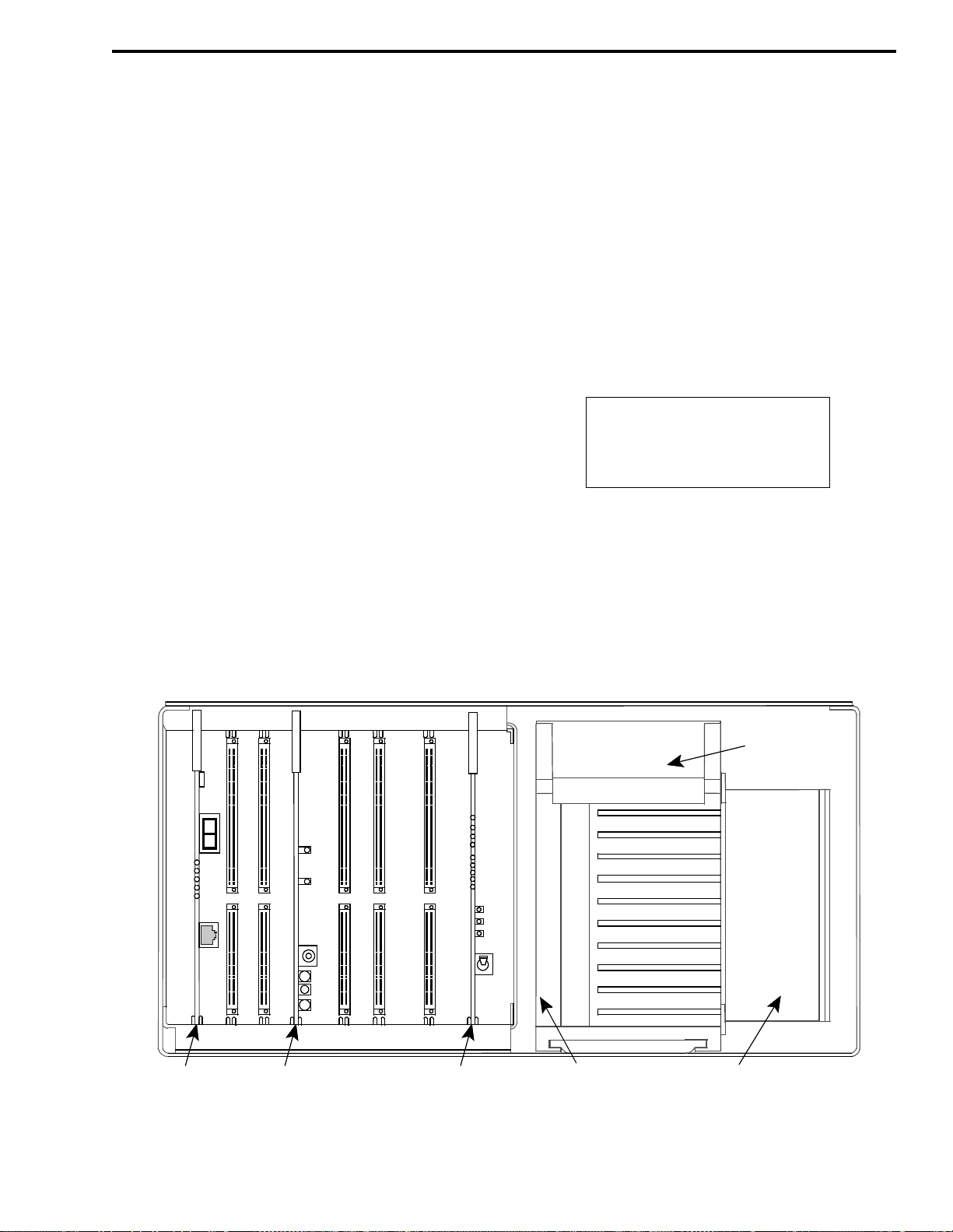
INTRODUCTION AND OPERATION
1.13 REPEATER OPERATION
1.13.1 MAIN PROCESSOR CARD (MPC)
Refer to Figure 1-2.
• Programming Jack
J1 provides input connection from the computer
and the "flash memory" in the MPC. The programming information in an IBM
PC programs the MPC
directly from the serial card through an interconnect
cable to the COM1 or COM2 port.
• Reset
S1 provides a manua l r eset of the Main Processor
Card (MPC). A manual reset causes a complete
power-up restart.
• Display and LEDs
Each combination of DS1 display read-out and
CR4/CR3 indication refers to an active alarm. See
T able 1- 2 for alarms and defi nitions . LED indications:
CR1 blinking; MPC is operational, CR2 on; high
power, of f is low power and CR5 on; in dicat es an LTR
Repeater.
1.13.2 TEST MODE
When the Repeater is in Test mode the safety
measures are disabled. Therefore, if the Repeater is
keyed for an extended period and the power amplifier
temperature increas e, thermal shutdown will not occur .
There are pop-up windows that appear in the Test
mode screens to alert the user that there is an alarm
and action should be taken.
RF Thermal Sense Alarm Con dition Exists
NOTE: Safety measures are disabled
Ok
Figure 1-1 ALARM IN TEST MODE
PROG
RESET
RF INTERFACE
BOARD
S1
DS1
GND
GRN
CR1
YEL
CR2
YEL
CR5
RED
CR4
RED
CR3
J1
JACK
J103
J100
SPKR
A D
LEVEL
LOCAL
ON/OFF/VOL
R236
MIC
J102
J101
J104
EXT SPKR
+15V
+15V ACC
-5V
+5V
CWID
HANG
SWITCH
MOBILE
XMIT
J500
TP
J501
GND
J502
+15V
S508
IACMACMPC
PA
EXCITER/RECEIVER
Figure 1-2 REPEATER CARDS
March 1999
1-5
Part No. 001-2009-600
Page 22

INTRODUCTION AND OPERATION
Table 1-2 ACTIVE REPEATER ALARMS
Alarm No. DS1 CR3 CR4 Definition
Test Mode
IAC input 1 Active
IAC input 2 Active
IAC input 3 Active
IAC input 4 Active
IAC input 5 Active
IAC input 6 Active
IAC input 7 Active
IAC input 8 Active
MAC Processor Alarm
HSDB Processor/Cable Alarm
IRDB Cable Alarm
TIC Processor Alarm
VNC Alarm
AC Power Failure
Battery Power Failure
Power supply thermal sense
Fan 1 current out of specification
Fan 2 current out of specification
IAC mismatch
RF shutdown
RF Half Power Mode
Thermal sense in RF portion
RF Finals 1-2 power out failure
RF Finals 3-4 power out failure
RF VSWR Failure
Normal Synthesizer Tx Lock failure
Normal Synthesizer Rx Lock failure
HS Synthesizer Tx Lock failure
HS Synthesizer Rx Lock failure
RF Quarter Power Alarm
10
11
13
15
16
17
18
19
20
21
32
33
34
35
36
37
38
39
40
41
42
0
1
2
3
4
5
6
7
8
9
0
1
2
3
4
5
6
7
8
9
A
B
D
F
0
1
2
3
4
5
0
1
2
3
4
5
6
7
8
9
A
Off
Off
Off
Off
Off
Off
Off
Off
Off
Off
Off
Off
Off
Off
On
On
On
On
On
On
On
On
On
On
On
On
On
On
On
On
On
On
On
On
On
On
On
On
On
On
On
On
On
On
On
Off
Off
Off
Off
Off
Off
On
On
On
On
On
On
On
On
On
On
On
March 1999
Part No. 001-2009-600
1-6
Page 23

INTRODUCTION AND OPERATION
1.13.3 MAIN AUDIO CARD (MAC)
Refer to Figure 1-2.
• External Speaker Jack
J104 provides repeater audi o output to an external
speaker. The local volume control adjusts the volume
level of this speaker.
• Speaker/Microphone Jacks
J102 provides audio input from a microphone.
J101 provides the receive audio to the microphone.
• Local On/O ff/Volume Control
R236 provides control o f the recei ve audi o output
to J101 and J104. Turning this control clockwise past
the detente applie s voltage t o the local audio amplif ier .
• A D Level Test Point
J100 provides audio/data level output for test
level checks.
• Power Supply On/Off Switch
S508 turns the power supply DC voltages on and
off from the IAC i n the front of the repeater.
• Power Indicator
CR501 indicates the +5V supply is at normal
level and applied to the IAC. CR524 indicates -5V
supply is at normal level and applied to the IAC.
CR523 indicates the +15V accessory supply is at normal level. CR525 indicates that the +15V supply is at
normal level and applied to the IAC.
• CWID Indicator
This indicates that the CW Identification is being
transmitted on the lowest-frequency repeater. The
CWID is a continuous-wave (CW) transmission of the
station call letters in Morse Code to satisfy the station
identification requi rement. The CWID is progr ammed
into the repeater memory. This indicator also is used
when an alarm is transmitted with Morse code.
• Hang Indicator
• Ground
J103 is connected to ground for test equipment
when monitoring test point J100.
1.13.4 INTERFACE ALARM CARD (IAC)
Refer to Figure 1-2.
• Voltage Test Output
J502 provides a +15V test point on the IAC.
• Ground
J501 is connected to ground for test equipment
when monitoring voltage test point J502.
• A D Level Test Point
J500 provides a test point to monitor audio and
data levels, AC fail and thermal sensor.
This indicates that the hang word is being transmitted by the repeater. This word is transmitted on
calls in which the channel is held for the duration of
the call and not just for the duration of the transmission. The hang word tells the mobiles to stay on the
same channel and not re-access the system when
responding to a call.
• Switch Call Indicator
The Switch Call Indicator on the IAC shows that
a Switch-To-Mobile transmission is in progress (see
Figure 7-30.)
• Mobile Call Indicator
Mobile-to-repeater transmission in progress is
indicated by the Mobile Call Indicator.
• Xmit Indicator
This indicates that the repeater transmitter is
keyed by the logic.
1-7
March 1999
Part No. 001-2009-600
Page 24

INTRODUCTION AND OPERATION
1.13.5 POWER SUPPLY
The 2000 Series Repeater Power Supply is a quad
output 800W supply with power factor correction. A
battery back-up module, PN 023-2000-830, can be
added to the power supply to provide automatic battery revert in the event of AC power failure (see Section 1.4) The Battery Back-Up module charges the
batteries when AC is present at the power supply (see
Section 1.5 and 8.6).
1.14 LTR-Net SYSTEM COMPONENTS
1.14.1 INTRODUCTION
The main components in a LTR-Net system are
shown in Figure 1-3. An LTR-Net system can be
designed to meet the requi reme nts of almost any user.
The following are LTR-Net features.
• With LTR-Net signaling, advance d feat ures suc h as
up to 65504 Unique ID codes, automatic mobile
identification, home cha nnel backup, and five levels
of access priority are available.
• Users of differen t types of ra dio equipment can talk
to each other.
Example: a Conventional mobile channel cou ld talk
to a mobile operating on a LTR-Net (trunked)
900 MHz channel.
• Wide area radio coverage can be provided so that a
mobile could talk to another mobile that is using a
repeater that may be hundreds of mil es away. That
repeater may be part of the same LTR-Net system or
another LTR-Net system. Phone line or other types
of links can be used to provide the communication
path.
LTR-Net systems are not restricted to a specific
type of signaling. Example : an ent ire LTR-Net system
could be designed using Conventional channels which
use tone- or digitally-controlled squelch. The various
types of signaling can also be mixed in a system.
Example: There could be:
Check with your Johnson represen tative for more
information concerning the capabilities of LTR-Net
systems.
The following sections provide a br ief descript ion
of the LTR-Net components see Figure 1-3.
1.14.2 MOBILE TRANSCEIVERS
The mobile and handheld transceivers used in a
LTR-Net system must be compatible with the type of
signaling in use and also the frequency range.
LTR-Net transceivers can be programmed for
LTR and Conventional operation. However, some
LTR transceivers can only be programmed for LTR
and Conventional operation. The main difference
between LTR-Net and LTR only versions of the same
model is the so ftware in the m icroprocessor.
1.14.3 REPEATERS
NOTE: The Summit QX does not require a
separate LTR-Net logic drawer.
The repeater model used in a LTR-Net system is
determined by frequency range, 900 MHz use the
Summit QX 2009 repeaters. There is one repeater for
each RF channel.
Inter-Repeater Data Communication
Data communication between LTR-Net or LTR
repeaters is via a high-speed data bus. This bus cable
is installed in a daisy-chain manner between repeaters. If both LTR-Net and LTR repeaters are located at
a Locality, only like types are connected together. Up
to 20 LTR-Net or 20 LTR repeaters can be interconnected (see Section 1.9 for connecting the data bus).
10-channels using LTR-Net signaling
5-channels using LTR
5-channels using Conventional signaling
March 1999
Part No. 001-2009-600
signaling
1-8
Page 25
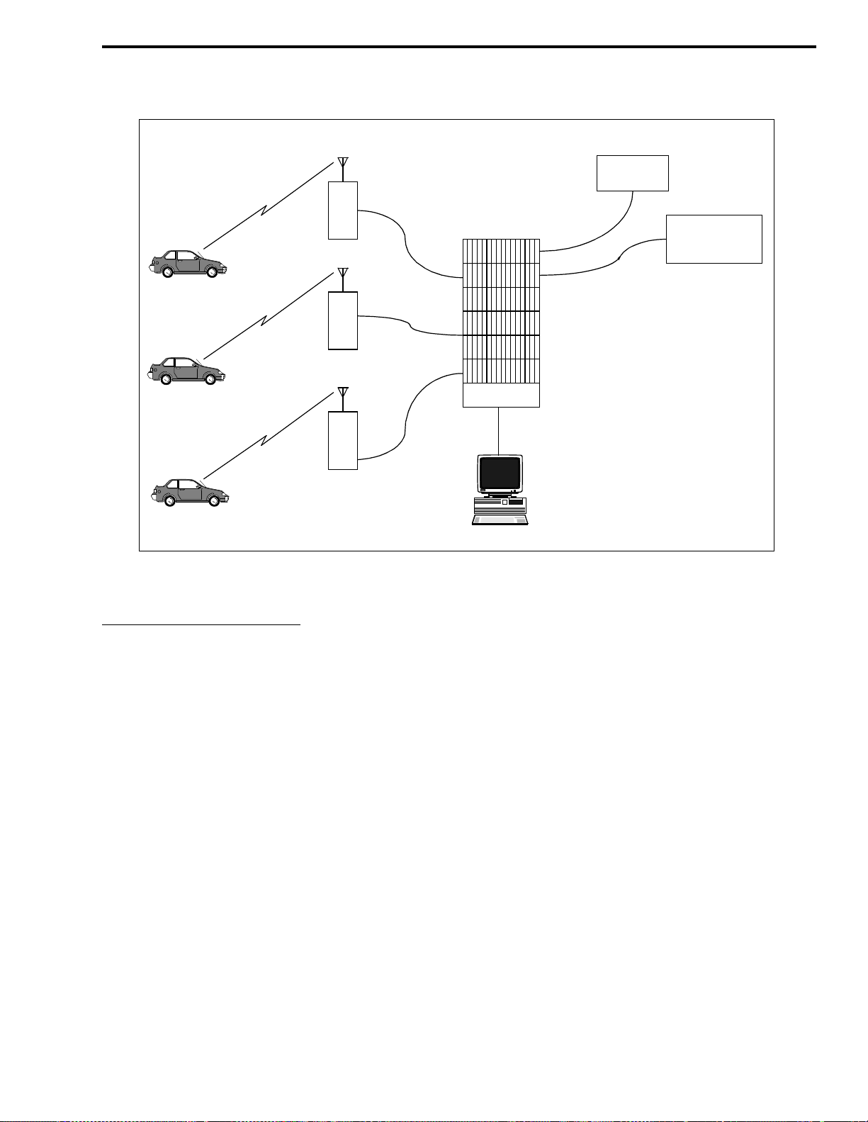
LTR-Net REPEATERS
(UP TO 20 PER SWITCH)
INTRODUCTION AND OPERATION
OTHER SWITCHES
AND SYSTEMS
AUDIO AND
DATA LINK
LTR-Net
MOBILE TRANSCEIVER
AUDIO AND
DATA LINK
LTR
MOBILE TRANSCEIVER
CONVENTIONAL
MOBILE TRANSCEIVER
AUDIO AND
DAT A LINK
SYSTEM and SUBSCRIBER MANAGER (SSM)
Figure 1-3 LTR-Net SYSTEM COMPONENTS
Repeater Connection To Switch
The repeaters can be located at the same Locality
as the Switch or they may be located at a Locality that
is many miles from the Switch. A voice and data link
is required between the repeaters and Switch. This
link can be a direct connection, phone lines, microwave, RF transceiver, fiber optic, or some other type
of link. This link is connected to the repeater terminal
block on the back of the repeater.
3000 SERIES SWITCH
CIM
CIM
CCM
WAM/SNM
TIM
NetNIM
PUBLIC SWITCHED
TELEPHONE NETWORK
(PSTN) OR PABX
required for the call. On Switch-to-mobile calls, the
data fed to the repeater allows the Switch to operate
the repeater like a base station.
There are three di f fere nt type s of links that can be
selected for the data path between each repeater and
the Switch. The MPC is programmed for the type of
link used (see Section 1.11).
The voice link routes transceiver voice to and
from the Switch. The voice must be routed to the
Switch when a call involves a dispatcher, telephone
interconnect, or another RF channel or LTR-Net system. If the call is a mobile-to-mobile call on the sam e
RF channel, the voice is simply repeated by the
repeater (it is also routed to the Switch but is not connected to anything). The voice path input/output port
interfaces with a standard 4-wire, 600 ohm phone line.
The data link allows the Switch to control the
repeater. With mobile-to-repeater calls, the data fed to
the Switch is used to dete rmine what r outing is
• A 4-Wire v oice-grade link ca n be used that is simi lar
to the audio link. The data is then sent as tones usi ng
FSK modulation.
• RS-232 serial inputs and outputs are available for
direct connection or connection to a l ink that accepts
RS-232 data.
• Data can be modulated as in ’1’ and then sent over
the voice path using a Blank and Burst technique.
Only one 4-wire link is then needed between each
repeater and the Switch.
March 1999
1-9
Part No. 001-2009-600
Page 26

INTRODUCTION AND OPERATION
1.14.4 SWITCH
The Switch can connect s everal di ff erent for ms of
communication together to form a communication network that requires the Call Processor. It has up to six
shelves with 12 or 16 device slots each (72 or 96 slots
available) and up to three racks (for 216 or 288 slots).
Many different modules are available to complete the
network. Some modules have specific device slot
requirements.
1.14.5 CALL PROCESSOR AND SYSTEM AND
SUBSCRIBER MANAGER
The Call Processor, along with the System and
Subscriber Manager, controls the LTR-Net System.
The Call Processor (CP) is an IBM
PC or compatible
computer that is running the EFJohnson management
program. The System and Subscriber Manager software is used b y the System Ad ministrator to program,
control and continuously monitor Switch operation,
and provides logging of information for billing purposes.
The System and Subscriber Manager (SSM) is a
program that executes on an IBM PC or compatible
computer. The function of the SSM is to manage the
database information tha t the Call Proces sor use s in it s
operation. The SSM has the capability to generate
reports from the logged information of the CP. The
SSM also has the ability to setup and initiate such
activities as Dynamic Reprogramming of certain
mobile parameters (Group 11), disabling (Kill) of lost
or stolen mobiles and many other functions.
1.14.6 LOCALITY
A Locality is the location where one or more
repeaters are housed. Trunked system repeaters are
connected to the same high-speed data bus and are
required to be located close together. LTR-Net can
have a maximum of 20 repeaters at a Locality. One
CIM (Channel Interface Module) is required for each
LTR-Net repeater. A CCM (Conventional Channel
Module) is required for a conventional channel.
1.14.7 HOME REPEATER CHANNEL
All LTR-Net mobiles have one of the Locality
repeaters assigned as their "Home Repeater". This
repeater handles the data and audio unless a failure
causes the Status Rep eat er to take ov er. The Group ID
calls use the Ho me Repeater number in ident if y i ng the
mobiles (see Section 1.15.3).
1.14.8 STATUS REPEATER CHANNEL
The Status Repeater Channel is one repeater at a
Locality designated to transmit update informat ion for
all calls occurr ing at that Locality. The Status repeater
is a "Home Repeater" backup usually not assigned
voice traffic.
1.14.9 MONITOR REPEATER CHANNEL
This is the repeater channel that a mobile is currently monitoring for upda te messages. This repeater
may be either the mobile’s Home Repeater or the
Locality Status Repeater. A special algorithm is used
by the mobile to determine which is to be monitored.
Generally, it is the last repeater that a valid data message was detected on.
1.14.10 HOME CHANNEL ALIASING
The LTR-Net Home Channel Aliasing feature
increases the number of addresses available on a
Locality for Group calls. It does this by allowing calls
to be programmed on non-exisent Home repeaters.
Each Home repeater can be programmed with 1239 Group ID codes. Assume a Locality has four
active repeaters and one of these is the Status repeater
(that is normally not assigned as a Home repeater).
The number of calls that can be programmed are then
as follows:
Without Aliasing - 3 x 239 or 717 calls
With Aliasing - 20 x 239 or 4780 calls
When a call is placed on a non-existent Home
repeater, the subscriber unit automatically uses the
next lower numbered active repeater.
NOTE: Since this feature does not increase system
capacity, adding too many users may result in unsatisfactory operation due to frequency busy conditions.
March 1999
Part No. 001-2009-600
1-10
Page 27

INTRODUCTION AND OPERATION
1.14.11 TELEPHONE INTERCONNECT AND DATA TRANSMISSION
Mobile transceivers can be used to access the
PSTN (Public Switched Telephone Network). However, this interconnect operation must be on a secondary basis to dispatch operation. An exception is when
the trunked system or channel is assigned exclusively
to one user.
Mobiles may place telephone calls through the
PSTN (Public Switch Telephone Network) or a PABX
(Private Automatic Branch E xchange) using the Interconnect special call. When the Call Processor detects
a mobile placing an interconnect ca ll, it checks to see
if it is authorized that service determined by the System and Subscriber Manager and what type of call it is
making. If it is authorized, the Switch completes the
connection through the TIM (Telephone Interface
Module) to the telephone networ k. The Call Process or
performs the record keeping needed for billing.
Data transmission and paging ar e also al lowed on
these frequencies. It also must be secondary to voice
communicati on. Refer to applicable FCC rules and
regulations fo r more information.
1.14.12 PUBLIC SWITCHED TELEPHONE NET-
WORK (PSTN)
If interconnect calls are to be placed by mobiles
or landside users to mobiles, the Switch is connected
to the PSTN (Public Switched Telephone Network).
The specific mobiles which can place calls and other
interconnect parameters are determined by how the
System Manager programs the System and Subscriber
Manager/Call Processor and by the programming of
each mobile transceiver.
1.14.13 PRIVATE AUTOMATIC BRANCH EX-
CHANGE (PABX)
The system has the ability to connect to a PABX
or PBX. This allows mobile orig inate d calls to use t he
dial access codes and the least cost routing facility of
the PABX/PBX.
1.14.14 PULSE CODE MODULATION (PCM)
PCM typically runs on the voice buses at 2.048
MHz. The Switch provides 32-Time Slots for sending
of audio.
1.15 LTR-Net FEATURES
1.15.1 STANDARD AND SPECIAL CALLS
There are two types of calls with LTR-Net signaling; Standard Calls and Special Cal ls. Group ID codes
1-239 are Standard (dispatch) calls, and Group ID
codes 240-247 are Special Calls.
As previously stated, up to 239 Group ID codes
are assignable on each Home repeater. When a transceiver monitors i ts Home o r S tat us repe ater, it receives
data messages containing a Home repeater number,
Group ID, and Unique ID code (refer to Section
1.15.2). When it detects its Home repeater and a
Group ID from 1-239 that i t i s prog rammed to decode,
it unsquelches and the call is received. The correct
Unique ID code does not need to be detected to
receive a Standard Call. Standard Calls are limited to
other transceivers assigned to the s ame Home repeater .
However, each selectable system of a transceiver can
be programmed with a different Home repeater to
allow calls to mobiles assigned to other Home repeaters if desired.
If a Group ID from 240-247 is r ecei ved, a Spec ial
Call is indicated and the transceiver will respond
according to the type of call. Special calls are used to
perform many of the special LTR-Net features
described in this section. Examples of Special Calls
are calls to a specific transceiver (Unique ID), Group
(Directed Group) or Telephone Interconnect. Others
are Interrogate, Interconnect, and Transceiver Disable. Generally, a transceiver must decode its Unique
ID code to respond to a Special Call.
1.15.2 UNIQUE ID CODES
Each transceiver is programmed with a Unique
ID code in addition to Group ID codes. Unique ID
codes are assigned on a system-wide basis, not on a
repeater basis as with Group IDs . Up to 655 04 Uni que
ID codes can be assigned per Switch.
Whenever a transceiver makes a call, it always
transmits its Uniqu e ID in a dditi on to a Group ID. Any
control point equipped with a decoder and display
capable of listeni ng to that transcei ver can th en displa y
the ID of that unit. This provides automatic identification of transceivers making calls.
March 1999
1-11
Part No. 001-2009-600
Page 28

INTRODUCTION AND OPERATION
Unique IDs also permit indivi dual mob ile un its t o
be called using the special calls described in the preceding section. Calls can also be made to individual
transceivers using standard call Group IDs 1-239 if an
ID is assigned to only one transceiver.
1.15.3 GROUP IDENTIFICATION CALLS
The Group ID (1-239) is assigned to each LTRNet Home Repeater. A "standard" Group ID call is
accepted by a mobile if its Home Repeater and Group
ID are in the data message. A "special" calls are Telephone Interconnect calls, UID calls and Directed
Group calls (Auxiliary calls). Telephone Interconnect
Calls are assigned a Token Group ID (240-247)
assigned by the repeater upon request from a mobile.
Telephone Interconnect calls, Unique ID calls and
Directed Group Calls all require the System and Subscriber Manager/Call Processor to provide authorization.
1.15.4 ALARM FORWARDING TO SWITCH
Repeater alarms are routed to the CIB (Channel
Interface Bus) t o be d etect ed by th e Call Proce ssor and
the System and Subscriber Manager.
March 1999
Part No. 001-2009-600
1-12
Page 29

SPECIFICATIONS
INTRODUCTION AND OPERATION
GENERAL
1
Frequency Range 896-901 MHz Receive, 935-940 MHz Tr ansmit
Dimensions 9.125 H x 17" W x 20.9" D
AC Voltage/Frequency 100-240V AC/50-60 Hz
AC Current (at 117V AC) 0.40A (Standby), 1.8A (25W), 3.3A (75W), 5.8A (160W)
AC Input Power 47W (Standby), 211W (25W), 390W (75W), 680W (160W)
DC Current at 26.5V DC 6A (25W), 11A (75W), 22.5A (160W)
Number of Channels 1 (Synthesized, programmable)
Channel Spacing 12.5 kHz
Channel Resolution 12.5 kHz
Temperature Range -30°C to +60°C (-22°F to +140°F)
Duty Cycle Continuous
FCC Type Acceptance ATH2422009, ATH2422009-1
FCC Compliance Parts 15, 90
RECEIVER
12 dB SINAD 0.35 µV
20 dB Quieting 0.50 µV
Signal Displacement Bandwidth ±3 kHz
Adjacent Channel Rejection -75 dB
Intermodulation Rejection -75 dB
Spurious & Image Rejection -90 dB
Audio Squelch Sensitivity 12 dB SINAD
Audio Response +1/-3 dB TIA
Audio Distortion Less than 3% at 0.5W/16 ohms
Local Audio Power 0.5W/16 ohms
Audio Sensitivity ±750 Hz
Hum & Noise Ratio -45 dB
Frequency Spread 5 MHz
Frequency Stability ±0.1 PPM -30°C to +60°C (-22°F to +140°F)
TRANSMITTER
RF Power Output Low Power = 75W min (default setting) 25W (variable set point)
High Power = 160W min (default setting) 75W (variable set point)
Spurious Emissions -90 dBc
Harmonic Emissions -90 dBc
Audio Deviation ±1.6 kHz
LTR Data Deviation ±750 Hz
CWID Deviation ±1 kHz
Repeat Deviation ±800 Hz
Audio Response +1/-3 dB TIA
Audio Distortion Less than 2%
Hum & Noise (TIA) -45 dB
Frequency Spread 5 MHz
Frequency Stability ±0.1 PPM -30°C to +60°C (-22°F to +140°F)
Emission Designators 11K0F3E, 11K0F1D
1. These general specifications are intended for reference and are subject to change without notice. Contact th e Systems
Applications consult ants for guaranteed or additional specifications.
March 1999
1-13
Part No. 001-2009-600
Page 30

INTRODUCTION AND OPERATION
2000 OCXO DRAWER
Size 1.75” high, 17” wide, 14” deep (19” rack mount, 1 rack unit height)
Weight 8 pounds
Shipping Weight 9 pounds
Operational Temperature Range -30°C to +60°C (-22°F to +140°F)
AC Voltage/Frequency 115V AC ±15% 50/60 Hz
DC Voltage (w/2 oscillators) 0.2A (115V AC) or 0.1A (230V AC)
DC Voltage (optiona external supply) 15V DC ±15%
DC Current (w/2 oscillators) < 1A DC at initial turn on
< 0.7A DC after warm-up
Frequency 10 MHz
Reference Signal Outputs 8 - 1.25 MHz outputs
External 10 MHz Signal Input Level 2V P-P minimum (high impendance input)
Output Amplitude 0 dBm ±1 dB (1.25 MHz outputs)
10 dBm ±1 dB (10 MHz output)
Overall Oscillator Output Stability 0.1 PPM
Oscillator Temperature Stability 0.03 PPM (-40°C to +70°C (-40°F to +158°F)
Oscillator Aging 1 E-9/Day
Oscillator Tuning Range (Mechanical) Range for 10 years aging adjustable to 0.01 PPM nominal
Single Sideband Noise/Hz -105 dBc at 10 Hz
-135 dBc at 100 Hz
-150 dBc at 10 kHz
Current handling capability of
alarm relay outputs 2A
March 1999
Part No. 001-2009-600
1-14
Page 31

SECTION 2 INSTALLATION
2.1 INTRODUCTION
Information in this section tells how to set up the
repeater for operation in an LTR-Net system. It is
assumed that the repeater has been previously aligned
at the factory or as described in the alignment procedure in Section 7.
Even though each repeater is thoroughly aligned
and tested at the factory, it is good practice to check
performance before it is placed in service. This
ensures that no damage occurred during shipment and
that the repeater is otherwise operating properly. Performance testing is described in Sections 7.2, 7.3, 7.4
and 7.5.
2.1.1 SITE PREPARA TION AND ANTENNA IN-
STALLATION
Site preparation and antenna installation are not
within the scope of this manual. Basic installation
requirements are discussed in the "Dealer Guide To
Site Preparation", Part No. 004-8000-100. Factory
installation is also available. Contact your Johnson
representativ e for more informa tion.
2.2 ENVIRONMENT
The following conditions should be consi dered
when selecting a site for the Repeater.
Operating Te mperature
-30°C to +60°C (-22°F to +140°F).
Humidity
Less than 95% relative humidity at 50°C.
Air Quality
For equipment operating in a controlled environment with the Repeaters rack mounted, the airborne
3
particles must not exceed 30 µg/m
.
For equipment operating in an uncontrolled environment with the Repeaters rack mounted, the airborne particles must not exceed 100 µg/m
3
.
NOTE: If the Repeater is installed in an area that
exceeds these environmental conditions, the site
should be equipped with air filters to remove dust and
dirt that could cause the equipment to overheat.
2.3 VENTILATION
The RF modules and the power supply are
equipped with fans, controlled by thermostats, that
force air through the equipment for cooling. The air
flow is from the front to the back of the equipment.
This permits the Repeaters to be stacked or rack
mounted (see Figure 2-3). There are a few considerations when installing Repeaters to provide adequate
air circulation.
• The Repeaters should b e mounted wit h a min imum
of 6 inches clearance between the front or back of
the cabinet for air flow. The power supply requires
a minimum of 18 inches at the back of the Rep eater
for removal.
NOTE: Repeaters should not touch. Leave a minimum of one empty screw hole (approximately 1/2")
between repeaters vertically, especially for bottom
ventilation slots in high power repeaters.
• Cabinet enclosures must provide air vents for ade-
quate air circulation.
• Temperature and humidity must be considered
when several Repeaters ar e installed at a site. This
might require air conditioning the site.
2.4 AC POWER
The AC power source to the V i king VX Repeater
can be 120V AC or 240V AC. Nothing need be done
to the power supply for 240V AC operation. However, a 240V AC outlet requires that the 120V AC
power plug be replaced. A locking AC power cord is
provided for the supply.
The 120V AC cord is a standa rd 3-wi re gro unded
cord used with a standard AC wall outlet. The outlet
must be capable of supplying a maximum of 328W (-
632) or 680W (-634). With the nominal 120V AC
input, the source must supply 3A for each 75W
2-1
March 1999
Part No. 001-2009-600
Page 32

INSTALLATION
B- B+ TEMP
ACTIVE
CHARGER
ON
CHARGER
FAULT
BATTERY
BATTERY
REVERSE
GROUND
EARTH
NEUTRAL
LINE
SWITCH
repeater or 6A for each 160W repeater and should be
protected by a circuit breaker. It is recommended that
all of the repeaters in a rack should not be on the same
breaker in order to provide one operational repeater in
the event a breaker trips. An AC surge protector is
recommended for all equipment.
Each Repeater requires an outlet, the receiver
multicoupler and OCXO drawer require one each, so
for a 5-channel system a minimum of 8 outlets are
required. An additional three should be added for test
equipment. The outlets must be within 3 feet of each
Repeater cabinet. Future system expansion should be
considered when electrical work is being planned for
the initial system.
The Viking VX Repeater power supply can be
equipped with an optional 24V DC back-up in the
event of AC po wer failure. Si nce the transmitter
remains on full power , if desired, the DC power source
must have a current capability of about 15A per 75W
repeater (25A per 160W repeater) or 75A for 5-75W
repeaters (125A for 5-160W repeaters). The multicoupler requires 0.5A and the OCXO drawer requires
1A for a total system requirement at 24V DC of 76.5A
for 75W repeaters (126.5A for 160W repeaters).
perature sensor cable is shown in Figure 2-2. LED
indicators are provided to show Reverse Battery connection, Charger On/Off and Battery Fault.
TEMP
NEGATIVE
BATTERY
TERMINAL
WHT
BLK
GND
Figure 2-2 TEMPERATURE SENSOR CABLE
2.6 800W POWER SUPPLY
The power supply has four voltage output levels
(see Table 2-1). Each voltage is set to ±1% at +25°C
(+77°F). The output of this supply is capable or running any 2000 series repeater.
Each output is overload protected such that the
power supply current limits and automatically resets
when the overload is removed (see Table 2-1).
Each output is over voltage protected such that
the power supply shuts down when an over voltage
condition exists, usually when a component in the supply has failed (see Table 2-2). The power supply must
be manually reset by toggling the Enable Line or
removing AC power for more than 10 seconds.
Figure 2-1 BATTERY BACKUP CONNECTOR
2.5 BATTERY BACKUP
If the power supply is equipped with battery
backup, screw lugs are provided on the front of the
power supply for battery connect ions (see Figure 2-2).
A switch is provide d f o r ch arging the battery or can be
off if a separ ate bat te ry cha rger is used. A battery temperature sensor connection is also provided. The tem-
March 1999
Part No. 001-2009-600
Table 2-1 OUTPUT VOLTAGES
Voltage Current Wattage
+26.5V 22A 583W
+15V 5A 75W
+5.2V 5A 26W
-5V 1A 5W
Table 2-2 OVER VOLTAGE
Voltage Range
+26.5V +32V to +33V
+15V +16V to +18V
+5.2V +6V to +7V
-5V -6V to -7V
2-2
Page 33

INSTALLATION
BACKPLANE
14
369
J2
A
2
4
1
3
5
B
6
7
852
10
7
11
8
12
9
C
J2
A
B
C
1
2
3
4
5
6
7
8
9
10
11
12
POWER HARNESS
+26.5V
GROUND
+15V
AC FAIL IN
POWER SWITCH
THERMAL SENSOR
N/C
+15V
N/C
N/C
+5V
-5V
TO
RFIB
2
1
4
5
3
9
6
8
7
REPEATER
BACKPLANE
POWER CABLE CONNECTOR AND SCHEMATIC
TO
2.6.1 AC INPUT REQUIREMENTS
AC Input Voltage: 100-240V AC
Line Frequency: 50-60 Hz
AC In-rush: 60A maximum
Overall Efficiency: >70% at 100V AC
>80% at 240V AC
Lightning protection: 6kV for < 1ms
Power Factor: >0.97 at full load
Brown Out Voltage: 80V AC
Temperature -30°C - +60°C (full power)
Power factor correction per IEC555. The Power
supply has the following safety agency approvals
pending: UL1950, CSA22.2-950, TUV EN60950
(IEC950)
When the AC input voltage is below 90V AC, the
maximum output power is decreased to keep the input
current constant. If a battery back-up is installed, the
batteries take over when the AC input voltage falls
below 80V AC (dependent on power output).
The AC input connector is an IEC connector
equipped with a locking mechanism.
The operating temperature range is -30°C to
+60°C (-22°F to +140° F), i.e. the sa me as the repeate r .
The fan is thermostatically controlled by the internal
temperature. When the internal heatsink temperature
reaches +45°C (113°F) the fan turns on. When the
heatsink temperature drops below +35°C (95°F) the
fan turns off. If the internal heatsink temperature
reaches +90°C (+194°F) the power supply turns off
until the heatsink temperature drops below +85°C
(+185°F). The over-temperature shutdown and restart
are automatic.
2.7 GROUNDING
CAUTION
PROPER SITE GROUNDING AND LIGHTNING
PROTECTION ARE VERY IMPORTANT TO PREVENT PERMANENT DAMAGE TO THE REPEATER.
As in any fixed radio installation, measures
should be taken to reduce the possibility of lightning
damage to the Viking VX equipment. Proper grounding eliminates shock hazard, protects against electromagnetic interference (EMI) and light ni ng.
2-3
March 1999
Part No. 001-2009-600
Page 34

INSTALLATION
Ground each piece of equipment separately. Do
not ground one piece o f eq uip ment by co nnecting it to
another grounded piece of equipment.
A good DC ground must be found or created at
the site. Rooftop site grounds can be researched
through the building management or architects.
Tower site grounds must be made with grounding
rods. The many techniques for providing adequate
grounds for towers and poles and for installing building ground bus lines are beyond the sc ope of this manual. Refer to National Electrical Code article 250
"Grounding Techniques," article 800 "Communications Systems" and follow local codes.
The ground bus should be routed to the floo r area
within 5 feet of the syst em with a run ner of 6 AWG or
larger solid copper wire or 8 AWG stranded copper
wire.
The outer conductor of each transmission line at
the point where it enters the building should be
grounded using 6 AWG or larger solid copper wire or
8 AWG stranded wire.
Secondary protection (other than grounding) provides the equipment protection against line transients
that result from lightning. There are two types of secondary protection, RF and Telephone Line. Use the
same wire sizes as specifi ed fo r co ax ial cables for any
ground connections required by the secondary protectors.
RF
An RF protector keeps any lightning strike to the
antenna feed line or tower from damaging the Repeaters. Install this protection in-line with the combiner
and antenna feed line.
RF protectors are selected by calculating the
maximum instantaneous voltage at the output of the
combiner. Do this by using the following equation.
V
= 1.414 (X) (√P(50))
P
Where:
V
= Voltage at the output of the combiner.
P
P = repeater output in wa tts
X= for VSWR=
1.05 1.10 : 1
1.09 1.20 : 1
1.13 1.30 : 1
1.17 1.40 : 1
1.20 1.50 : 1
1.30 1.86 : 1
Example: Repeater power output of 60W with a
VSWR of 1.3 : 1 (for this VSWR, X = 1.13):
V
= 1.414 (1.13) (√60(50))
P
V
= 1.59782 (√60(50))
P
V
= 1.59782 (54.772256)
P
V
= 87.52V
P
Telephone Line
There are four typ es of pr otect ion su ppre ssors fo r
telephone lines; Gas Tube, Silicon Avalanche Diode,
Metal Oxide Varistor and Hybrid.
The hybrid protector is ideal for EF Johnson
equipment, and is strongly recommended. A hybrid
suppressor combines several forms of protection not
available in just one type of device. For example, a
high-speed diode reacts fir st cla mping a vol ta ge st ri ke
within 10 ns, a heavy duty heat coil reacts next to
reduce the remainder of the current surge, and a highpowered three-element gas tube fires, grounding Tip
and Ring.
2.7.1 PROTECTION GUIDELINES
Follow these guidelines for grounding and lightning protection. Each Repeater installation site is different; all of these may not apply.
• Ensure that ground connections make good metal-
to-metal contact (e.g. grounding rod or tray, metal
conduit) using #6 gauge soli d or braided wire straps.
• With surge protectors, ensure that ground wires go
directly to ground, not through other equipment.
• Run the ground wire for RF coax protec tors directly
to ground.
• With coax protectors, ensure maximum instanta-
neous voltage does not exceed the rated voltage.
March 1999
Part No. 001-2009-600
2-4
Page 35

• Do not run ground wire s parallel to any other wirin g
(e.g. a ground wire parallel to a telephone line),
except other ground wires.
• Double check all equipment for good ground and
that all connections are clean and secure.
2.8 UNPACKING AND INSPECTION
The Repeater is shipped securely crated for transportation. When the Repeater arrives, ensure the
crates remain upright, especially if storing the crates
temporarily.
When unpacking the Repeater, check for any visible damage or problems caused by shipping. If there
is obvious damage from shipping mishaps, file claims
with the carrier. If there appears to be any damage
caused before shipping, file a claim with Transcrypt
International, Inc . Cont act Cust omer Ser v i ce f or ass istance (see Section 1.8).
If everything appears undamaged, remove the
Repeater equipment from the crate, using normal precautions for unpacking.
NOTE: Do not discard the packing materials. If you
must return an item, use the same packing materials
and methods (including static protective bags for circuit cards) to repack the equipment. You are responsible for proper repacking. Transcrypt International,
Inc. cannot be responsible for damage to equipment
caused by negligence.
INSTALLATION
TM
OCXO1
OCXO2
DELTA F
OUTPUT
AC
DC
DC BACKUP
INTERRUPT
OCXO 1
INTERRUPT
OCXO 2
INTERRUPT
T
X
C
O
M
B
I
N
E
R
D
U
PL
E
X
E
R
R
X
M
U
L
T
I
C
O
U
PO
PL
E
W
R
E
R
S
T
R
I
P
NOTE: Repeaters should not touch. Leave a minimum of one empty screw hole (approximately 1/2")
between repeaters vertically, especially for bottom
ventilation slots in high power repeaters.
NOTE: Each repeater should be grounded separately
by connecting a ground bus from the ground lug on the
back side of the RF module to the ground bar on the
rack (see Figure 2-7).
Figure 2-3 RACK MOUNTED REPEATERS
2-5
Part No. 001-2009-600
March 1999
Page 36

INSTALLATION
123
4
1
234567
8
ONLY VIKING VX REPEATERS
ONLY VIKING VX END REPEATERS
(CENTER REPEATERS)
ON
ON
2
1
87
6
5
4
3
2
143
S3 S2
ON
2
143
S3
ON
2
1
8
7
6
5
4
3
T/R ANTENNA
RECEIVER 1
RECEIVER 2
RECEIVER 3
RECEIVER 4
RECEIVER 5
RECEIVER
MULTICOUPLER
Figure 2-4 5-CHANNEL COMBINING SYSTEM
2.9 REPEATER DATA BUS INSTALLATION
The repeaters are interconnected by a balanced
line High-Speed Data Bus (HSDB) consisting of a six
conductor cable. The total length of the HSDB cannot
exceed 500 feet. Connect the cables in daisy-chain
fashion to modular connector A5 on the back of the
repeater (see Figure 2-16). A 50 ohm termination is
not required for VIKING VX repeaters.
2.9.1 MPC DATA BUS SWITCH SETTINGS
TRANSMITTER 1
DUPLEXER
BANDPAS S
FILTER
PREAMPLIFIER
TRANSMITTER
COMBINER
TRANSMITTER 2
TRANSMITTER 3
TRANSMITTER 4
TRANSMITTER 5
2.9.2 MPC DATA BUS JUMPER SETTINGS
Refer to Figure 2-6 for crystal selection and
HSDB Code selections jumper placement. Jumper
J5, pins 1-2 selects 11.059 MHz for LTR-Net (J5, pins
2-3 selects 12 MHz crystal for Standard LTR). The
jumper on J4, pins 5-6 connects EPROM U14, pin 27
to ground for LTR-Net (J4, pins 3-4 connects EPROM
U14, pin 27 (A14) to +5V for Standard LTR singleended 5V data bus).
Switch settings on the MPC for the two types of
installations r equi re S2 and S3 sections to be s wit ched
as indicated in Figure 2-5.
Figure 2-5 MPC DATA BUS SWITCHES
March 1999
Part No. 001-2009-600
CRYSTAL SELECTION
1
J5
23
HSDB CODE SELECTION
46
J4
123
5
Figure 2-6 MPC JUMPERS
Jumper J4 must be placed with the following
guidelines: J4, pins 5-6 for ope ration wit h the RJ-1 1 to
RJ-11 cable 200X systems (see Section 4.5.6).
2-6
Page 37

INSTALLATION
2.10 CONNECTING RECEIVE AND TRANSMIT ANTENNAS
Receive and Transmit antenna connector locations are shown in Figure 2-7. Although each transmitter and receiver could be connected to a separate
antenna, this is usually not done because of the large
number of antennas required by a multiple repeater
installation. Therefore, an antenna combining system
is usually used. An example of a combining system
for a five-channel sy ste m is s hown i n Fig u re 2-4 . The
amount of power loss introduced by a combiner
depends on the type of combiner used. If it has a loss
of 3 dB, power output to the antenna is reduced by
half.
GROUND
RX
TX
Connect the voice link to terminals 1-2 and 3-4
(see Figure 2-8 and 2-12).
P1-31
P1-63
VOICE LINK CONNECTIONS
FSK BLANK/B U RS T
TO SWITCH
RXA
P1-32
2
4
P1-64
A-
X
T
RIN
1
3
+
A
+
RX
TXA
TIP
TIP 1
EA
MA
RXS+
D
S+
X
T
T IN
VOT AU
D
A
N
EXT REQ1
D
U
C
V
O
R
AC
G
5V
1
+
SI
S
R
1 I
D
N
U
O
R
G
+15V ACC
AC FAIL
1 IN -
2 IN -
1 OUT -
UT
O
2
ALARMS
34
G
1
G
RIN
EB
B
M
RXS-
TXS-
EXT MOD
J2
Figure 2-8 TERMINAL BLOCK J2
2.11.2 DATA L INK
+
N
+
N
2 I
1 OUT +
UT +
O
2
33
-
Figure 2-7 ANTENNA CONNECTIONS
2.11 CONNECTING AUDIO/DATA LINK TO SWITCH
A communication link of some type is required
between the Switch and each repeater. This link
allows the Switch to control the repeater and also
routes audio between the Swi tch and rep eater. V arious
types of links can be used, such as phone line, RF
transceiver , micr owave, or f iber o ptic Re fer t o Secti on
1.14.3 for more information. The repeater connection
point is terminal block J 2 on the back panel (see Figures 2-8, 2-12 and 2-13). The information which follows describes the installation of these links.
2.11.1 VOICE LINK
The voice link is always connected and it should
be a standard 4-wire, 600 ohm balanced voice- grade
link. It can be non-metallic, i.e. DC continuity is not
required. If the r epeat ers a nd Switc h are located at the
same site, direct conne cti on c an be use d as l ong as t he
line is less than approximately 300 feet.
One of these three methods can be used for
installing the data link.
NOTE: See Section 7 for Link Alignment.
1. Separate 4-wire link can be u sed that is similar to
that used for voice. The data is then encoded by
FSK and sent as tones.
8
TX
7
)
D
-
N
S
G
(
X
-
S
X
R
S
X
R
4
+
S
K
FS
)
R
O
I
D
)
U
D
A
(
N
+
-
S
X
R
R
S
1
3
2
O
N
)
G
K
(
S
F
(
-
+
S
S
X
X
T
D
U
A
(
+
S
S
TX
TX
0
1
1
S
6
1
0
5
0
4
3
2
O
)
O
I
)
K
FS
(
+
N
Figure 2-9 MAC DIP SWITCH SETTINGS FOR
4-WIRE LINK
March 1999
2-7
Part No. 001-2009-600
1
Page 38

INSTALLATION
O
N
2
1
8
7
6
5
4
3
O
N
2
1
4
3
R
X
S
-
(
G
N
D
)
R
X
S
-
R
X
S
+
(
A
U
D
I
O
)
R
X
S
+
(
FS
K
)
R
X
S
-
(
G
N
D
)
TX
S
-
TX
S
+
(
A
U
D
I
O
)
TX
S
+
(
FS
K
)
S
1
0
0
S
1
0
1
F
S
K
T
X
S
+
O
N
2
1
8
7
6
5
4
3
O
N
2
1
4
3
R
X
S
-
(
G
N
D
)
R
X
S
-
R
X
S
+
(
A
U
D
I
O
)
R
X
S
+
(
F
S
K
)
R
X
S
-
(
G
N
D
)
TX
S
-
T
X
S
+
(
A
U
D
I
O
)
TX
S
+
(
F
S
K
)
S
10
0
S
10
1
F
S
K
TX
S
+
2. A separate RS-232 serial link can be used.
LTR-Net
REPEATER
RxA+
RxA-
VOICE LINK CONNECTIONS
J2-1
J2-2
P1-31
P1-32
SWITCH
RxA+
RxA-
PRIMARY
RxA
Figure 2-10 MAC DIP SWITCH SETTINGS
FOR RS-232 LINK
3. The FSK data can be sent over the voice link using
a Blank and Burst tec hni que . No separate data link
is then required.
TxA+
TxA-
LTR-Net
REPEATER
RxS+
RxS-
TxS+
TxS-
J2-3
J2-4
DATA LINK CONNECTIONS
J2-13
J2-14
J2-15
J2-16
P1-63
P1-64
P1-27
P1-28
P1-59
P1-60
TxA+
TxA-
SWITCH
RxS+
RxS-
TxS+
TxS-
PRIMARY
TxA
SECONDARY
RxA
SECONDARY
TxA
Figure 2-12 LTR-Net VOICE/DATA LINK
2.12 OCXO DRAWER CONNECTIONS
2.12.1 VIKING VX CONNECTION
These guidelines should be followed when using
2009 series repeaters with a 2000 OCXO drawer, Part
No. 023-2000-925.
Figure 2-11 MAC DIP SWITCH SETTINGS
2-8 and 2-12 and make the connections to terminals 12 and 3-4.
March 1999
Part No. 001-2009-600
Select the type of link being used, refer to Figure
FOR BLANK AND BURST LINK
• One 1.25 MHz output on the 2000 OCXO drawer is
connected to the 1.25 MHz Input on each 2009
Repeater. Up to eight 2009 series repeaters can be
connected to the 1.25 MHz Output ports.
This level is approximately 0 dBm.
• If connection to additional 2009 series repeaters is
necessary, additional 8-Way Splitter Shelves, Part
No. 023-2000-924, are added as required.
All shelves are connected to the 1.25 MHz output
ports of the 2000 OCXO drawer.
The level at the s pl itter shelf output por ts is approximately -10 dBm. See Figure 2-13.
2-8
Page 39

A010 IN SPLITTER SHELF
INSTALLATION
20dB
J1
ATTENUATOR
INPUT
20dB
J1
ATTENUATOR
INPUT
20dB
J1
ATTENUATOR
INPUT
10dB
J3
J2
10dB
J4
J5
36 dB AT TENUATION
10dB
J2
J3
10dB
J4
J5
23 dB AT TENUATION
10dB
J2
J3
10dB
J4
J5
19 dB ATTENUATION
6dB
J6
J7
6dB
J6
J7
6dB
J6
J7
3dB
OUTPUT
J9
J8
J8
J8
J10
3dB
OUTPUT
J9
J10
3dB
OUTPUT
J9
J10
Figure 2-13 ATTENUATOR SETTINGS
2-9
March 1999
Part No. 001-2009-600
Page 40

INSTALLATION
1.25 MHz
OUTPUTS
10 MHz
1.25 MHz
TO GPS 10 MHz
SERIES 2000 OCXO DRAWER (023-2000-925)
115V
B+
B-
TEMP
MPC SWITCHES/JUMPERS
HSDB CODE
ON21876543ON2143
SELECTION
S3
J4
S2
123
46
5
Figure 2-14 SINGLE REPEATER INSTALLATION
10 MHz SPLITTER
+12V
1.25 MHz
OUTPUTS
TO GPS 10 MHz
SERIES 2000 OC XO DRAWER (023-2000-925)
115V
CRYSTAL
SELECTION
231J5
10 MHz
B- B+ TEMP
1.25 MHz
MPC SWITCHES/JUMPERS
2143
ON
2
4
3
1
S3
10 MHz
1.25 MHz
S2
MPC SWITCHES/JUMPERS
ON
2143
S3
2
4
3
1
S2
8765
ON
8765
HSDB CODE
SELECTION
J4
ON
J4
46
123
5
B- B+ TEMP
HSDB CODE
SELECTION
46
123
5
CRYSTAL
SELECTION
231J5
CRYSTAL
SELECTION
231J5
March 1999
Part No. 001-2009-600
Figure 2-15 TWO REPEATER INSTALLATION
2-10
Page 41

+12V
10 MHz
1.25 MHz
1.25 MHz
OUTPUTS
INSTALLATION
10 MHz SPLITTER
TO GPS 10 MHz
SERIES 2000 OC XO DRAWER (023-2000-925)
115V
B- B+ TEMP
END REPEATER
2
14
3
S3
2
3
1
ON
S2
10 MHz
1.25 MHz
MIDDLE REPEATERS
2
143
S3
ON
10 MHz
1.25 MHz
2
1
S2
MPC SWITCHES/JUMPERS
4
HSDB CODE
SELECTION
8765
ON
46
J4
123
5
B- B+ TEMP
MPC SWITCHES/JUMPERS
HSDB CODE
6543
7
SELECTION
8
ON
46
J4
123
5
B- B+ TEMP
CRYSTAL
SELECTION
231J5
CRYSTAL
SELECTION
231J5
END REPEATER
2
143
S3
1
ON
2
MPC SWITCHES/JUMPERS
HSDB CODE
43
S2
SELECTION
8765
ON
46
J4
123
CRYSTAL
SELECTION
5
231J5
Figure 2-16 THREE OR MORE REPEATERS INSTALLATION
2-11
March 1999
Part No. 001-2009-600
Page 42

INSTALLATION
0 dBm
+12V
1.25 MHz
OUTPUTS
10 MHz
1.25 MHz
10 MHz
1.25 MHz
10 MHz
1.25 MHz
10 MHz SPLITTER
TO GPS 10 MHz
SERIES 2000 OCXO DRAWER (023-2000-925)
115V
B- B+TEMP
B- B+TEMP
B- B+TEMP
1 PPS CONNECTION FROM GPS
0 dBm
HSDB
ALL MIDDLE REPEATERS
HSDB CODE
J4
21
3
4
ON
S3
SELECTION
123465 231J5
1
2
S2
CRYSTAL
SELECTION
-10 dBm
876543
ON
HSDB
+12V
SPLIT IN
1.25 MHz
INPUT
10 MHz SPLITTER
8-WAY SPLITTER SHELF (023-2000-924)
OUTPUTS
1.25 MHz
B- B+TEMP
B- B+TEMP
B- B+TEMP
10 MHz
1.25 MHz
10 MHz
1.25 MHz
HSDB
B- B+TEMP
HSDB
10 MHz
END REPEATERS
B- B+TEMP
MPC SWITCHES/JUMPERS
END REPEATER
1
S3
HSDB CODE
SELECTION
J4
4
2
3
ON
123465 231J5
2
43
1
S2
CRYSTAL
SELECTION
8765
ON
1.25 MHz
Figure 2-17 MORE THAN ONE RACK OF LTR-Net REPEATERS
B- B+TEMP
B- B+TEMP
March 1999
Part No. 001-2009-600
2-12
Page 43

SECTION 3 SOFTWARE
Figure 3-1 PROGRAMMING SETUP
3.1 INTRODUCTION
3.1.1 PROGRAMMING SETUP
The following items are required to program the
repeater. The part numbers of this equipment are
shown in Section 1, Table 1-1. A programming setup
is shown above.
The LTR-Net Programmer on 3.5 inch disk, Part
No. 023-9998-459, uses Windows NT 4.0 or later, or
Windows 95 or later on a personal computer to program the EEPROM Memory in the Main Processor
Card (MPC ).
The computer is connected directly from the
serial card to the MPC. The interconnect cables used
are shown in Figure 3-2. The DB-9 to 8-pin modular
adapter is connected to the serial port of the computer
and an interconnect cable connects the adapter to the
MPC.
NOTE: These connections are for the IBM computer
and may differ from an IBM compatible. In which
case, consult the manuals for your computer f or serial
card outputs and connections.
3.1.2 MINIMUM COMPUTER REQUIREMENTS
The LTR-Net Programmer requires W indo ws NT
4.0 or later, or Windows 95 or later that meets the following minimum requirements.
• 16M of memory
• 486 or faster microprocessor
• The personality prog ram and hel p fil e are suppl ied
on a 3.5", 1.44M diskette only. Therefore, a computer with a hard disk drive and 3.5" (1.44M) flop py
drive is requi red.
• One unused serial port
• Color monitor
Although the program uses color to highlight certain areas o n the screen, a monochrome (black and
white) monitor or LCD laptop also provide satisfactory operation. Most video fo rmats are support ed. An
unused serial port is required to connect the repeater
to the computer. One or two serial ports are standard
with most computers. One port may be used by the
mouse.
3-1
March 1999
Part No. 001-2009-600
Page 44

SOFTWARE
3.1.3 PROGRAMMING CABLES
The cables from the repeater to the computer are
not included.
TO MPC
TO LAPTOP
Figure 3-2 LAPTOP INTERCONNECT CABLE
3.1.4 EEPROM DATA STORAGE
The data programmed into the MPC is stored by
an EEPROM memory. Since this type of device is
nonvolatile, data is stored indefinitely without the
need for a constant power supply. A repeater can be
removed from the site or even stored indefinitely with out affecting programming. Since EEPROM memory
is also reprogrammabl e, a new device is not needed if
programming is changed.
The LTR-Net Programmer is used to configure
repeaters for proper operation with the LTR-Net
protocol.
From the repeater stan dpoint, a n LTR-Net system
consists of one or more r epeaters installed in a Locality, a 3000 Series Switch and the necessary interconnects and programming to provide LTR-Net operation
(see Section 1).
The LTR-Net Programmer defaults to using
COM1 at 9600 baud to communicate with a repeater,
however this can be changed by selecting Utilities ->
COM Port Setup from the menu, or by clicking on the
COM toolbar button (see Section 4.7.1).
When you first start the programmer, you should
create a Loca lity file with th e information you wish to
program into repeaters at that Locality. See "How Do
I ... Create A New Locality File" for information on
performing this function.
NOTE: All repeaters installed in a given Locality use
the same Locality informat ion, but each has its unique
repeater information programmed.
3.1.6 LIMITATIONS
3.1.5 GETTING STARTED
NOTE: Before starting you should already know
how to start Windows NT
, format and make backup
copies of disks, copy and delete files, and run programs. If you ar e u nfamiliar with any o f these a ctions,
refer to the Windows NT manual for your computer for
more information (see Section 5).
Follow the computer instructions for loading the
disk. The computer needs to have RS-232C capability, for example, the Serial Card in slot "COM1" or
"COM2".
March 1999
Part No. 001-2009-600
The LTR-Net Programmer requires W indo ws NT
4.0 or later, or Windows 95 or later.
In order to read data from a repeater, a Locality
file must first be loaded from disk, or create and save
a Locality file. Only one Locality file may be loaded
at a time.
The LTR-Net Programmer supports COM1
through COM4, and all of the baud rates currently
supported by the MPC. Si nce th e nu mb er of d at a bi ts ,
stop bits, and the parity are fixed in the MPC, these
cannot be changed in the programmer.
3-2
Page 45

SOFTWARE
3.2 MISCELLANEOUS SOFTWARE INFORMATION
3.2.1 MINIMUM FREE MEMORY REQUIRED
Approximately 2MB of free memory is required
to run this program. If not enough is available, there
may be other programs t hat are also being loaded into
conventional memory. These programs can be closed
to make mor e space available.
3.2.2 SOFTWARE INSTALLATION
• Making a Backup Copy
When the programming software is received,
make a backup copy and store the master in a safe
place. To make a copy of the distribution disk with
Windows NT or Windows 95 Explorer, right click the
floppy drive icon and select Copy Disk.
• Creating a Windows Shortcut or Program Icon
To run the program from Windows NT or Windows 95, a shortcut icon can be created that can then
be double clicked to start the program. To create this
shortcut icon, select Start -> Settings -> Taskbar.
Then select the S ta rt Me nu Pro gra ms ta b and c li ck t he
Add button. Information is then displayed to complete the process.
Once files have been opened or saved from
within the programmer, those filenames will show up
in the taskbar Documents selection. allowing the program to be started by selecting the desired Locality
file from the Start menu.
Refer to Sect ion 4 for detailed information about
the LTR-Net Programmer’s cont en ts and Section 5 for
the parameters and their descriptions for the Locality
and Repeater programming.
3.3 ALIGNMENT SOFTWARE
The software for the LTR-Net repeater programs
the MPC to open and close the audio/data gates necessary for the alignment selected from the Test-Full
Repeater menu.
Under the menu heading TEST, are the alignment
procedures for the PA (see Section 7.4 or 7.5),
Receiver (see Section 7.2), Exciter (see Section 7.3)
and overall Full Repeater (see Section 7.6) including
the MAC card (see Figure 3-3).
3.2.3 STARTING THE PROGRAM
There are several ways to start the LTR-Net Programmer. First, the program can be started by double
clicking on the shortcut icon. This starts the program
with an empty information file (Locality file). A
Locality file contains all of the programming information for all repeaters installed at a L ocality.
A second method of star ting the program is to use
the Explorer to change to the directory containing
Locality files, the n do ubl e cl ic k on one of those Locality files. This starts the programmer and automatically loads the sel ected file. This i s norm ally t he mos t
convenient method to star t the progr am, as it pre-loa ds
all of the repeater data for a Locality.
Figure 3-3 REPEATER TEST MENU
Refer to Section 7 for alignment procedures as
shown in the program, alignment points diagrams and
test setup d iagrams.
3.4 HELP
Help screens are available for most parameters
and options in this progr am. Whenever a parameter or
options clarification is needed, press the Help button
and a help screen will pop-up on the screen.
March 1999
3-3
Part No. 001-2009-600
Page 46

SOFTWARE
FILE
New* Ctrl+N
Open* Ctrl+O
Save As
Save* Ctrl+S
[Files List]
Exit
Locality Information*
Define Repeaters
Adjacent Locality Data
EDIT
TRANSFER
HARDWARE
TEST
UTILITIES
VIEW
Select Repeater*
Repeater Information*
Delete Repeater
Read Setup Parameters*
Write Setup Parameters*
HSDB Monitor*
Rx/Tx Data
RF Data
Input Monitor
Revisions*
Mode Select
Exciter
PA
Receiver
Full Repeater
Adjust RNT Link
COM Port Setup*
Alarm Display
Status Bar
Tool Bar
Save Settings On Exit
Edit Parameters
General Parameters
Input Alarms
Output Alarms
Alarm Cross Reference
All Tests
Repeater Setup
Transmitter Test
Receiver Test
Transmit Audio/Data
Audio Data Adjust
Repeater Operations
HELP
March 1999
Part No. 001-2009-600
Help Topics
Help On Help
About LTR-Net
* Denotes an associated icon in the Tool Bar
Figure 3-4 PROGRAMMING FLOWCHART
3-4
Page 47

SECTION 4 LTR-Net PROGRAMMER
4.1 MENU DISPLAYS
The menus available are listed at the top of the
screen (see Figure 4-1). Move the cursor with the
mouse to highlight the menu name. Press the left
mouse key to view the menu and the mouse to scroll
through the menu. Call up the highlighted selection
by pressing the left mouse button. The Toolbar provides one-click access to some of the most frequently
used menu selections.
Figure 4-1 MAIN MENU
4.2 FILE MENU
This menu manipulates new or existing files into
directories and saves files to be called up at another
time.
4.2.2 OPEN
This menu selection has an equi valent icon in
the toolbar and shortcut key Ctrl+O. This
menu selection or icon opens a Locality file
and loads its information into the programme r. It
brings up a list of Locality data files to select fro m.
4.2.3 SAVE AS
This menu selection saves the edited version of
an existing fi le loaded in the buffer under a new filename or gives a new file created in the Edit menu a
filename.
Figure 4-2 FILE MENU
4.2.1 NEW
This menu selection has an equivalent icon
in the toolbar and shortc ut key Ctrl+ N. This
menu selection or icon erases all Locality
and Repeater information i n the progr ammer and loads
factory defaults. If t he current data has been changed,
selecting File -> Ne w or the i con pro vides t he o pportu nity to save the data before loading the defaults.
Figure 4-3 OPEN / SAVE AS / SAVE FILE
4.2.4 SAVE
This menu selection has an equivalent icon
in the toolbar and shortcut key Ctrl+S.
4.2.5 EXIT
Exits the rep eater program and returns to Windows NT. See Section 4.8.3, View -> Save Setting On
Exit to save the toolbar location (size and shape) as
well as the main window location and size when the
programmer is opened.
March 1999
4-1
Part No. 001-2009-600
Page 48

LTR-Net PROGRAMMER
Locality Information
Select Repeater
EDIT
Repeater Information
Delete Repeater
Figure 4-4 EDIT PROGRAMMING FLOWCHART
4.3 EDIT
This menu is used to create new files and set or
change the re peater operating parameters. The filename for the Locality and relevant data is shown in the
Title Bar and Status Bar (see Section 4.8.1).
Define Repeaters
Adjacent Locality Data
Edit Parameters
General Parameters
Input Alarms
Output Alarms
Alarm Cross Reference
4.3.1 LOCALITY INFORMATION
This menu selection has an equivalen t icon in
the toolbar. This menu selection or icon
brings up the Locality information screens to
Define Repeaters and Adjacent Localities.
Figure 4-5 EDIT MENU
Figure 4-6 LOCALITY CONFIGURAITON
Table 4-1 DEFINE REPEATERS PARAMETERS
Delete Entry Removes the selected Defined Repeater from the list.
Frequency Band Selects the Locality frequency band, 800 MHz, 800 MHz with offset, (or 900 MHz).
Channel Number Select a repeater number in the Defined Repeater pane and assign the channel number (1-920).
See Appendix A for an 800 MHz Frequency Chart.
Area Bit If the coverage area includes more than one Switch the area bit is used, this is normally 0.
Transmit Frequency This is displayed for reference and is determined when the Channel Number is selected.
Receive Frequency This is displayed for reference and is determined when the Channel Number is selected.
Active Click on this box to activate the selected Defined Repeater.
Defined Repeaters Click on a repeater number, then select the channel number and the data is displayed.
OK Saves the current selections shown and closes the window.
Cancel Disregards all changes and closes the window.
Help Displays the Help screen for the parameters in this window.
March 1999
Part No. 001-2009-600
4-2
Page 49

LTR-Net PROGRAMMER
4.3.2 SELECT REPEATE R
This menu selection h as an equival ent icon i n
the toolbar. This menu selection or icon se-
lects a repeater from the currently defined repeaters within this Loc ality (see Figure 4- 8). Move the
cursor with the mouse to highlight the repeater filename and double-click t he mouse to open the Edit Para meters window.
Figure 4-7 ADJACENT LOCALITY DA TA
• Select the Locality ID number for the Locality cur-
rently being defined.
• Select a Locality I D for each of the clos est Adjacent
Localities (0-15).
• Select a Preference number for each Adjacent
Locality number as an a lter nativ e when leav ing th e
range of this Locality.
Table 4-2 ADJACENT LOCALITY PARAMETERS
This Locality ID 0-1023 This is the ID of the Locality currently being defined.
Locality 0-1023 The Locality ID number of a neighboring Locality.
Preference 1-15 A scale number for the best alternative Locality (1 = Highest, 15 = Lowest).
# (Number) 0-15 Choice of 16 neighboring Localities that can pick-up transmissions.
Figure 4-8 SELECT REPEATER
4-3
March 1999
Part No. 001-2009-600
Page 50

LTR-Net PROGRAMMER
4.3.3 REPEATER INFORMATIO N
This menu selection has an equivalent icon in the toolbar. This menu selection or icon brings up the
parameter pages for the selected repeater. It allows entry of information specific to this repeater.
Figure 4-9 REPEATER CONFIGURATION
Table 4-3 GENERAL PARAMETERS
Repeater Number 1-20 Repeater number was established in Locality Configu ration.
Channel Number 1-399 Channel number was established in Locality Configuration.
Receive Frequency Frequency was determined by channel number in Locality Configuration.
Transmit Frequency Frequency was determined by channel number in Locality Configuration.
Test Mode ID 1-239 Group ID transmitted when the Repeater is in the Test Mode.
Local Mic ID 1-239 Group ID transmitted when the local microphone PTT is active.
Status Free 0=never
20=always
RNT Link None
FSK
Dig
BnB
RF Power Level Low, High Low=25-75, High=75-160. Power level in watts for transmit power output.
Options Stand Alone Selected if the repeater is permitted to operate without a connection to the 3000
High Stability Synth Selected if the Receiver and Transmitter use the High Stability Synthesizer.
Allow LTR Selected if standard LTR protocol is allowed.
Status Channel One repeater at a Locality is designated to transmit update information for all
Alarm to CIB Routes repeater alarms to the Channel Interface Bus to be detected by the Call
HSDB All Data Repeater receives all the data on the High Speed Data Bus.
Xmit Channel Info Repeater sends updates on all repeaters installed in this Locality.
Power Source AC, DC The type of primary power source for the Repeater.
CWID Time 0=disabled, 1-30 min The time interval between CWID transmissions.
CWID Message Station call letters This is the FCC station call letters (15 characters/numbers).
OK Saves the current selections shown and closes the window.
Cancel Disregards all changes on any of these four screens and closes the window.
Help Displays the Help screen for the parameters in this window.
When the number of free channels falls below this value, Status Channel can be
used for voice.
Data Signaling type for 3000 Series Switch.
Frequency Shift Keying
RS-232
Blank and Burst (FSK)
Series Switch.
calls occurring at that Locality. Normally not assigned as a Home repeater.
Processor and the System and Subscriber Manager.
March 1999
Part No. 001-2009-600
4-4
Page 51

LTR-Net PROGRAMMER
Figure 4-10 INPUT ALARMS
Input Alarms
There are four Input Alarms that can be activated
by external devices (see Section 6.13). These inputs
can be Disabled, Energized or De-Energized. Alarms
3 and 4 can also be Analog Inputs.
• Disabled - The input alarm line is inactive.
• Energized - An open circui t exter nal to th e repeat er
activates the alarm.
• De-energized - A closed circuit external to the
repeater activates the ala rm.
• Analog - Select the Low and High Limit pairs to trip
an Analog Input Alarm. The High Limit must be
greater in value than the Low Limit (0.0V-5.0V in
0.1V steps).
• Alarm Description - This is a text string (up to 15
characters) t o describe the alarm. The d escription is
automatically changed on the Cross Refere nce W in dow .
Figure 4-11 OUTPUT ALARMS
Output Alarms
Select the operation of the Output Alarm. The
available types are:
• Open Active - An active alarm opens (no contact)
the output lines.
• Closed Active - An acti ve alarm closes ( contact) the
output line s.
• Alarm Message
This is a text s tring (up to 15 characters) to
describe the alarm. This text string is sent via Morse
code if the alarm input is programmed with a Tx ID
and an output is selected in the Cross Reference menu
(see Figure 4-13). The Alarm Message is automatically transferred to the Cross Reference window.
• Transmit ID
Each of the 4-alarm outputs can be assigned a
Group ID from 1-239. The default setting is 238,
0 (zero) for disabled. This Group ID and the Repeater
number identify an alarm that is active. This ID can
be programmed into a transceiver so that when the
alarm is active, the alarm description is received in
Morse code.
• Alarm Transmit Rate
This sets the time interval for transmittin g the
alarm message in Morse code (0-30 min). If more
than one alarm is active, this is the inter-alarm time.
4-5
Part No. 001-2009-600
March 1999
Page 52

LTR-Net PROGRAMMER
Cross Reference
The cross reference screen selects the Output
Alarm that is activated by each Input Alarm.
There are up to:
• 48 alarms (0-47)
• 4 (hardware) External Input Alarms
• 18 (software) Internal Alarms (see Ta ble 1-2).
• 26 unused
There are 4 Output Alarms. An alarm condition
on any input can cause an Output Alarm. This window configures which Input Al arm activates an Output
Alarm.
NOTE: More than one alarm condition can share the
same output alarm (see Figure 4-13).
Show Alarm Map
This window displays an Alarm Map that displays those Alarm Outputs that have been mapped in
bold type. Double-clicking on these outputs lists the
Alarm Inputs that have been assigned to that output.
Figure 4-12 ALARM MAPPING
March 1999
Part No. 001-2009-600
Figure 4-13 ALARM CROSS REFERENCE
4-6
Page 53

LTR-Net PROGRAMMER
4.3.4 DELETE REPEATER
Select the Repeater num ber to delete from this
Locality and press the Delete button.
Figure 4-14 DELETE REPEATER
4.4 TRANSFER
Figure 4-15 TRANSFER MENU
4.4.1 READ SETUP PARAMETERS
This menu selection has an equivalent icon in
the toolbar. This menu selection or icon reads
the contents of the EEPROM memory of a repeater and loads it into a buffer. The contents of the
buffer may then be di splayed to show the p rogramming
of the repeater.
NOTE: This button is only available if a Locality file is
loaded and a repeater is connected.
HARDWARE
4.4.2 WRITE SETUP PARAMETERS
This menu selection has an equivalent icon in
the toolbar. This menu selection or icon sends
the contents of a Locali ty file to a connected re peater and programs the EEPROM memory in the Main
Processor Card (MPC).
HSDB Monitor
RX/TX Data
RF Data
Input Monitor
Revisions
Mode Select
Figure 4-16 HARDWARE PROGRAMMING FLOWCHART
4-7
March 1999
Part No. 001-2009-600
Page 54

LTR-Net PROGRAMMER
4.5 HARDWARE
Figure 4-17 HARDWARE MENU
The Home column refers to the Home repeater
number of the originator, therefore, the Repeater and
Home numbers may not be the same number. The GID
column refers to the Group ID of the talk group of the
originator. The UID is the Unique ID used to identify
the originator of Special Calls. Special Call information is listed in the Token and Subtype columns.
4.5.2 RECEIVE/TRANSMIT DATA
This is an information screen used at the repeater
Locality while the computer (laptop) is connected to
the MPC in the repeater being monitored (see Figure
4-19). This in formation is co ntained in the receive
data stream exchanged between the repeater and the
destination user (mobile/portable) and the data content of the repeat er tr ans m it da ta stream. The message
contains data received from the destination and data
sent to the mobile/portable by the repeater. The
repeater receives the destination’s: Unique ID, Home
Repeater Number, Group ID, Priority and Status. The
time stamp is included b ecause mess ages are sent continually and this provides a reference for when a data
exchange took place. The information sent to the destination in the update message from the repeater
includes: Description/Group, Channel In Use, Home
Repeater Number, Free Channel and Time Stamp.
Figure 4-18 HSDB MONITOR
4.5.1 HSDB MONITOR
This menu selection has an equivalent icon in
the toolbar . This menu selection or icon bri ngs
up the monitor window to view information
from the High Speed Data Bus (HSDB). The HSDB
connects all repeaters at a Locality and continually
sends updates on the status of each repeat er . This information window provides a list of all re peaters (1 to 20)
at the Locality. If a repeater is not sending data, IDLE
is next to the repeater numbe r. The data sent by the repeater is used to deter mine the Home, GID and UID of
destination (mobil e) users to receive the cal l pl ace d by
the originat or.
March 1999
Part No. 001-2009-600
Figure 4-19 REPEATER TRAFFIC MONITOR
4-8
Page 55

LTR-Net PROGRAMMER
4.5.3 RF DATA
Figure 4-20 RF DATA
The RF Line Monitor window shows the state of
the lines (see Figure 4-19). These lines are monitored
by the A-D converter in the IAC. The normal values
for each line are defined as follows.
4.5.4 INPUT MONITOR
This window m onitors the two Analog Input
lines. It is only used with the 4-Alarm Type IAC, and
only if Input 3, Input 4 or both are programmed for
"Analog". In addition to the actual or measured value,
the Low/High limit data are also displayed. These
limits are programmed in the "Edit -> Repeater Information -> Input Alarms" screen (see Figure 4-13). If
one of these inputs is not programmed "Analog", the
data for that input is blanked.
Figure 4-21 INPUT MONITOR
Synthesizer Lock Lines:
Exciter Synthesizer Yes, No
Receive Synthesizer Yes, No
Exciter High Stability Yes, No
Receive High Stability Yes, No
Wideband Audio Output approx. 200
LO Injection approx. 200
RSSI 20-150
Fan 1 Current 100-200, 0
Fan 2 Current 100-200, 0
Transmit Parameters:
Forward Power (Low Power 25-75 Watts
Forward Power (High Power) 75-175 Watts
Reflected Power 0-6 Watts
Final Out 1-2 (ratio) approx. equal
Final Out 3-4 (ratio) approx. equal
Chassis Temp 27°C-55°C
Fan On or Off
Power Supply Temp 22°C-45°C
Battery Voltage 21V-28V
Values with no label are the actual A-D reading.
To calculate the voltage on the line, divide the value
by 51. Example: Value ÷ 51 = Volts. Any variation
from the above values may indicate a problem in that
area. Values in this window are relative measur ements
only .
4.5.5 REVISIONS
This menu selection has an equivalent icon in
the toolbar. This menu selection or icon dis-
plays the cu rrent firmware revision information for the MPC, MAC and HSDB. The format is R.V
(revision.version) for all modules. The MPC information also includes the release date of the software and
the serial number of the repea ter . The HSDB version in
Figure 4-22 is for J4, pins 5-6 connected in the MPC for
LTR-Net (J4, pins 3-4 connected in the MPC are for
standard LTR).
Figure 4-22 REVISIONS
4-9
March 1999
Part No. 001-2009-600
Page 56

LTR-Net PROGRAMMER
4.5.6 MODE SELECT
The Mode Select window places the repeater
either in the Normal mode, Test mode or Diagnostic
mode. In the Normal mode, the repeater operates as a
normal repeater. In the Test mode or Diagno stic Mod e
the repeater transmits a test word. This test word is
the Test Mode ID setup in the Repeater Information
(see Section 4.3.3
).
C A U T I O N
While in the test or diagnostics mode the repeater is
"Busy", therefore it is important to place the repeater
in Normal mode when the Test Mode is no longer
required.
Figure 4-23 MODE SELECT
4.6 TEST
TEST
Exciter
PA
Receiver
Full Repeater
Adjust Switch Link
All Tests
Repeater Setup
Transmitter Test
Receiver Test
Transmit Audio/Data
Audio Data Adjust
Repeater Operations
Figure 4-24 TEST PROGRAMMING FLOWCHART
Figure 4-25 TEST MENU
March 1999
Part No. 001-2009-600
NOTE: Some screens may require scrolling down to
read the complete procedure.
4-10
Page 57

LTR-Net PROGRAMMER
4.6.1 EXCITER
This menu selection walks through the Exciter
alignment windows. Refer to Section 7.3 for the
Exciter alignment and Figure 7-2 for an alignment
points diagram and Figure 7-10 for a test setup of the
Exciter.
4.6.2 POWER AMPLIFIER
This menu selection walks through the Power
Amplifier and RF Inte rface Board alignment windows.
Refer to Sections 7.4 and 7.5 for the PA and RFIB
alignment in this manual and Figures 7-3, 7-4, and 7-5
for alignment points diagrams and Figures 7-11 and 78 of the Powe r Amplifier.
4.6.3 RECEIVER
This menu selection walks through the Receiver
alignment windows. Refer to Section 7.2 for the
Receiver alignment in this manual and Figure 7-1 for
an alignment points diagram and Figure 7-9 of the
Receiver.
4.7.1 COM PORT SETUP
This menu selection has an equivalent icon in
the toolbar . This menu selection or icon allows
changes to the COM port or baud rate used to
send and receive data from the attached Repe ater MPC.
An interface cable connect s the Repeater to the computer (see Figure 4-27).
Figure 4-27 SETUP COM PORT
4.6.4 FULL REPEATER
This menu selection walks through the full
repeater alignment windows. The Receiver and
Exciter portions are performance tests and adjustments. The Audio and Data portions are level adjustments for the Main Audio Card (MAC). Refer to Figure 7-28 for an alignment points diagram for the
MAC.
4.7 UTILITIES
Figure 4-26 UTILITIES MENU
4.7.2 ALARM DISPLAY
Figure 4-28 ALARM MONITOR
4-11
March 1999
Part No. 001-2009-600
Page 58

LTR-Net PROGRAMMER
4.8 VIEW
4.8.1 STATUS BAR
The Status Bar is located at the bottom of the
screen that displays information about the repeater.
4.8.2 TOOLBAR
The toolbar may be detached (floating) from the
main window by dragging the toolbar to a new location with the mouse. It may also be resized (and
reshaped) to suit individual preferences. The toolbar
may also be moved to any edge of the programmer
screen in this manner.
4.8.3 SAVE SETTINGS ON EXIT
When the menu item View -> Save Settings on
Exit is selected, the toolba r location (size and shape)
as well as the main window lo cation an d size are saved
and re-used when the programmer is opened.
4.9 HELP
4.9.1 HELP TOPICS
This window contains the contents file of help
topics, the index of help topics and a find topic screen.
4.9.2 HELP ON HELP
This window provides information on how to use
help.
4.9.3 ABOUT LTR-NET
ICON Definitions (left to right)
ICON Menu see Section
File -> New 4.2.1
File -> Open 4.2.2
File -> Save 4.2.4
Edit -> Locality Information 4.3.1
Edit -> Select Repeater 4.3.2
Edit -> Repeater Information 4.3.3
Transfer -> Read Setup Parameters 4.4.1
Transfer -> Write Setup Paramete rs 4.4.2
Hardware -> HSDB Monitor 4.5.1
Hardware -> Revisions 4.5.5
This menu selection provides information about
the programmer software.
Utilities -> COM Port 4.7.1
March 1999
Part No. 001-2009-600
4-12
Page 59

SECTION 4 LTR-Net PROGRAMMER
4.1 MENU DISPLAYS
The menus available are listed at the top of the
screen (see Figure 4-1). Move the cursor with the
mouse to highlight the menu name. Press the left
mouse key to view the menu and the mouse to scroll
through the menu. Call up the highlighted selection
by pressing the left mouse button. The Toolbar provides one-click access to some of the most frequently
used menu selections.
Figure 4-1 MAIN MENU
4.2 FILE MENU
This menu manipulates new or existing files into
directories and saves files to be called up at another
time.
4.2.2 OPEN
This menu selection has an equi valent icon in
the toolbar and shortcut key Ctrl+O. This
menu selection or icon opens a Locality file
and loads its information into the programme r. It
brings up a list of Locality data files to select fro m.
4.2.3 SAVE AS
This menu selection saves the edited version of
an existing fi le loaded in the buffer under a new filename or gives a new file created in the Edit menu a
filename.
Figure 4-2 FILE MENU
4.2.1 NEW
This menu selection has an equivalent icon
in the toolbar and shortc ut key Ctrl+ N. This
menu selection or icon erases all Locality
and Repeater information i n the progr ammer and loads
factory defaults. If t he current data has been changed,
selecting File -> Ne w or the i con pro vides t he o pportu nity to save the data before loading the defaults.
Figure 4-3 OPEN / SAVE AS / SAVE FILE
4.2.4 SAVE
This menu selection has an equivalent icon
in the toolbar and shortcut key Ctrl+S.
4.2.5 EXIT
Exits the rep eater program and returns to Windows NT. See Section 4.8.3, View -> Save Setting On
Exit to save the toolbar location (size and shape) as
well as the main window location and size when the
programmer is opened.
March 1999
4-1
Part No. 001-2009-600
Page 60

LTR-Net PROGRAMMER
Locality Information
Select Repeater
EDIT
Repeater Information
Delete Repeater
Figure 4-4 EDIT PROGRAMMING FLOWCHART
4.3 EDIT
This menu is used to create new files and set or
change the re peater operating parameters. The filename for the Locality and relevant data is shown in the
Title Bar and Status Bar (see Section 4.8.1).
Define Repeaters
Adjacent Locality Data
Edit Parameters
General Parameters
Input Alarms
Output Alarms
Alarm Cross Reference
4.3.1 LOCALITY INFORMATION
This menu selection has an equivalen t icon in
the toolbar. This menu selection or icon
brings up the Locality information screens to
Define Repeaters and Adjacent Localities.
Figure 4-5 EDIT MENU
Figure 4-6 LOCALITY CONFIGURAITON
Table 4-1 DEFINE REPEATERS PARAMETERS
Delete Entry Removes the selected Defined Repeater from the list.
Frequency Band Selects the Locality frequency band, 800 MHz, 800 MHz with offset, (or 900 MHz).
Channel Number Select a repeater number in the Defined Repeater pane and assign the channel number (1-920).
See Appendix A for an 800 MHz Frequency Chart.
Area Bit If the coverage area includes more than one Switch the area bit is used, this is normally 0.
Transmit Frequency This is displayed for reference and is determined when the Channel Number is selected.
Receive Frequency This is displayed for reference and is determined when the Channel Number is selected.
Active Click on this box to activate the selected Defined Repeater.
Defined Repeaters Click on a repeater number, then select the channel number and the data is displayed.
OK Saves the current selections shown and closes the window.
Cancel Disregards all changes and closes the window.
Help Displays the Help screen for the parameters in this window.
March 1999
Part No. 001-2009-600
4-2
Page 61

LTR-Net PROGRAMMER
4.3.2 SELECT REPEATE R
This menu selection h as an equival ent icon i n
the toolbar. This menu selection or icon se-
lects a repeater from the currently defined repeaters within this Loc ality (see Figure 4- 8). Move the
cursor with the mouse to highlight the repeater filename and double-click t he mouse to open the Edit Para meters window.
Figure 4-7 ADJACENT LOCALITY DA TA
• Select the Locality ID number for the Locality cur-
rently being defined.
• Select a Locality I D for each of the clos est Adjacent
Localities (0-15).
• Select a Preference number for each Adjacent
Locality number as an a lter nativ e when leav ing th e
range of this Locality.
Table 4-2 ADJACENT LOCALITY PARAMETERS
This Locality ID 0-1023 This is the ID of the Locality currently being defined.
Locality 0-1023 The Locality ID number of a neighboring Locality.
Preference 1-15 A scale number for the best alternative Locality (1 = Highest, 15 = Lowest).
# (Number) 0-15 Choice of 16 neighboring Localities that can pick-up transmissions.
Figure 4-8 SELECT REPEATER
4-3
March 1999
Part No. 001-2009-600
Page 62

LTR-Net PROGRAMMER
4.3.3 REPEATER INFORMATIO N
This menu selection has an equivalent icon in the toolbar. This menu selection or icon brings up the
parameter pages for the selected repeater. It allows entry of information specific to this repeater.
Figure 4-9 REPEATER CONFIGURATION
Table 4-3 GENERAL PARAMETERS
Repeater Number 1-20 Repeater number was established in Locality Configu ration.
Channel Number 1-399 Channel number was established in Locality Configuration.
Receive Frequency Frequency was determined by channel number in Locality Configuration.
Transmit Frequency Frequency was determined by channel number in Locality Configuration.
Test Mode ID 1-239 Group ID transmitted when the Repeater is in the Test Mode.
Local Mic ID 1-239 Group ID transmitted when the local microphone PTT is active.
Status Free 0=never
20=always
RNT Link None
FSK
Dig
BnB
RF Power Level Low, High Low=25-75, High=75-160. Power level in watts for transmit power output.
Options Stand Alone Selected if the repeater is permitted to operate without a connection to the 3000
High Stability Synth Selected if the Receiver and Transmitter use the High Stability Synthesizer.
Allow LTR Selected if standard LTR protocol is allowed.
Status Channel One repeater at a Locality is designated to transmit update information for all
Alarm to CIB Routes repeater alarms to the Channel Interface Bus to be detected by the Call
HSDB All Data Repeater receives all the data on the High Speed Data Bus.
Xmit Channel Info Repeater sends updates on all repeaters installed in this Locality.
Power Source AC, DC The type of primary power source for the Repeater.
CWID Time 0=disabled, 1-30 min The time interval between CWID transmissions.
CWID Message Station call letters This is the FCC station call letters (15 characters/numbers).
OK Saves the current selections shown and closes the window.
Cancel Disregards all changes on any of these four screens and closes the window.
Help Displays the Help screen for the parameters in this window.
When the number of free channels falls below this value, Status Channel can be
used for voice.
Data Signaling type for 3000 Series Switch.
Frequency Shift Keying
RS-232
Blank and Burst (FSK)
Series Switch.
calls occurring at that Locality. Normally not assigned as a Home repeater.
Processor and the System and Subscriber Manager.
March 1999
Part No. 001-2009-600
4-4
Page 63

LTR-Net PROGRAMMER
Figure 4-10 INPUT ALARMS
Input Alarms
There are four Input Alarms that can be activated
by external devices (see Section 6.13). These inputs
can be Disabled, Energized or De-Energized. Alarms
3 and 4 can also be Analog Inputs.
• Disabled - The input alarm line is inactive.
• Energized - An open circui t exter nal to th e repeat er
activates the alarm.
• De-energized - A closed circuit external to the
repeater activates the ala rm.
• Analog - Select the Low and High Limit pairs to trip
an Analog Input Alarm. The High Limit must be
greater in value than the Low Limit (0.0V-5.0V in
0.1V steps).
• Alarm Description - This is a text string (up to 15
characters) t o describe the alarm. The d escription is
automatically changed on the Cross Refere nce W in dow .
Figure 4-11 OUTPUT ALARMS
Output Alarms
Select the operation of the Output Alarm. The
available types are:
• Open Active - An active alarm opens (no contact)
the output lines.
• Closed Active - An acti ve alarm closes ( contact) the
output line s.
• Alarm Message
This is a text s tring (up to 15 characters) to
describe the alarm. This text string is sent via Morse
code if the alarm input is programmed with a Tx ID
and an output is selected in the Cross Reference menu
(see Figure 4-13). The Alarm Message is automatically transferred to the Cross Reference window.
• Transmit ID
Each of the 4-alarm outputs can be assigned a
Group ID from 1-239. The default setting is 238,
0 (zero) for disabled. This Group ID and the Repeater
number identify an alarm that is active. This ID can
be programmed into a transceiver so that when the
alarm is active, the alarm description is received in
Morse code.
• Alarm Transmit Rate
This sets the time interval for transmittin g the
alarm message in Morse code (0-30 min). If more
than one alarm is active, this is the inter-alarm time.
4-5
Part No. 001-2009-600
March 1999
Page 64

LTR-Net PROGRAMMER
Cross Reference
The cross reference screen selects the Output
Alarm that is activated by each Input Alarm.
There are up to:
• 48 alarms (0-47)
• 4 (hardware) External Input Alarms
• 18 (software) Internal Alarms (see Ta ble 1-2).
• 26 unused
There are 4 Output Alarms. An alarm condition
on any input can cause an Output Alarm. This window configures which Input Al arm activates an Output
Alarm.
NOTE: More than one alarm condition can share the
same output alarm (see Figure 4-13).
Show Alarm Map
This window displays an Alarm Map that displays those Alarm Outputs that have been mapped in
bold type. Double-clicking on these outputs lists the
Alarm Inputs that have been assigned to that output.
Figure 4-12 ALARM MAPPING
March 1999
Part No. 001-2009-600
Figure 4-13 ALARM CROSS REFERENCE
4-6
Page 65

LTR-Net PROGRAMMER
4.3.4 DELETE REPEATER
Select the Repeater num ber to delete from this
Locality and press the Delete button.
Figure 4-14 DELETE REPEATER
4.4 TRANSFER
Figure 4-15 TRANSFER MENU
4.4.1 READ SETUP PARAMETERS
This menu selection has an equivalent icon in
the toolbar. This menu selection or icon reads
the contents of the EEPROM memory of a repeater and loads it into a buffer. The contents of the
buffer may then be di splayed to show the p rogramming
of the repeater.
NOTE: This button is only available if a Locality file is
loaded and a repeater is connected.
HARDWARE
4.4.2 WRITE SETUP PARAMETERS
This menu selection has an equivalent icon in
the toolbar. This menu selection or icon sends
the contents of a Locali ty file to a connected re peater and programs the EEPROM memory in the Main
Processor Card (MPC).
HSDB Monitor
RX/TX Data
RF Data
Input Monitor
Revisions
Mode Select
Figure 4-16 HARDWARE PROGRAMMING FLOWCHART
4-7
March 1999
Part No. 001-2009-600
Page 66

LTR-Net PROGRAMMER
4.5 HARDWARE
Figure 4-17 HARDWARE MENU
The Home column refers to the Home repeater
number of the originator, therefore, the Repeater and
Home numbers may not be the same number. The GID
column refers to the Group ID of the talk group of the
originator. The UID is the Unique ID used to identify
the originator of Special Calls. Special Call information is listed in the Token and Subtype columns.
4.5.2 RECEIVE/TRANSMIT DATA
This is an information screen used at the repeater
Locality while the computer (laptop) is connected to
the MPC in the repeater being monitored (see Figure
4-19). This in formation is co ntained in the receive
data stream exchanged between the repeater and the
destination user (mobile/portable) and the data content of the repeat er tr ans m it da ta stream. The message
contains data received from the destination and data
sent to the mobile/portable by the repeater. The
repeater receives the destination’s: Unique ID, Home
Repeater Number, Group ID, Priority and Status. The
time stamp is included b ecause mess ages are sent continually and this provides a reference for when a data
exchange took place. The information sent to the destination in the update message from the repeater
includes: Description/Group, Channel In Use, Home
Repeater Number, Free Channel and Time Stamp.
Figure 4-18 HSDB MONITOR
4.5.1 HSDB MONITOR
This menu selection has an equivalent icon in
the toolbar . This menu selection or icon bri ngs
up the monitor window to view information
from the High Speed Data Bus (HSDB). The HSDB
connects all repeaters at a Locality and continually
sends updates on the status of each repeat er . This information window provides a list of all re peaters (1 to 20)
at the Locality. If a repeater is not sending data, IDLE
is next to the repeater numbe r. The data sent by the repeater is used to deter mine the Home, GID and UID of
destination (mobil e) users to receive the cal l pl ace d by
the originat or.
March 1999
Part No. 001-2009-600
Figure 4-19 REPEATER TRAFFIC MONITOR
4-8
Page 67

LTR-Net PROGRAMMER
4.5.3 RF DATA
Figure 4-20 RF DATA
The RF Line Monitor window shows the state of
the lines (see Figure 4-19). These lines are monitored
by the A-D converter in the IAC. The normal values
for each line are defined as follows.
4.5.4 INPUT MONITOR
This window m onitors the two Analog Input
lines. It is only used with the 4-Alarm Type IAC, and
only if Input 3, Input 4 or both are programmed for
"Analog". In addition to the actual or measured value,
the Low/High limit data are also displayed. These
limits are programmed in the "Edit -> Repeater Information -> Input Alarms" screen (see Figure 4-13). If
one of these inputs is not programmed "Analog", the
data for that input is blanked.
Figure 4-21 INPUT MONITOR
Synthesizer Lock Lines:
Exciter Synthesizer Yes, No
Receive Synthesizer Yes, No
Exciter High Stability Yes, No
Receive High Stability Yes, No
Wideband Audio Output approx. 200
LO Injection approx. 200
RSSI 20-150
Fan 1 Current 100-200, 0
Fan 2 Current 100-200, 0
Transmit Parameters:
Forward Power (Low Power 25-75 Watts
Forward Power (High Power) 75-175 Watts
Reflected Power 0-6 Watts
Final Out 1-2 (ratio) approx. equal
Final Out 3-4 (ratio) approx. equal
Chassis Temp 27°C-55°C
Fan On or Off
Power Supply Temp 22°C-45°C
Battery Voltage 21V-28V
Values with no label are the actual A-D reading.
To calculate the voltage on the line, divide the value
by 51. Example: Value ÷ 51 = Volts. Any variation
from the above values may indicate a problem in that
area. Values in this window are relative measur ements
only .
4.5.5 REVISIONS
This menu selection has an equivalent icon in
the toolbar. This menu selection or icon dis-
plays the cu rrent firmware revision information for the MPC, MAC and HSDB. The format is R.V
(revision.version) for all modules. The MPC information also includes the release date of the software and
the serial number of the repea ter . The HSDB version in
Figure 4-22 is for J4, pins 5-6 connected in the MPC for
LTR-Net (J4, pins 3-4 connected in the MPC are for
standard LTR).
Figure 4-22 REVISIONS
4-9
March 1999
Part No. 001-2009-600
Page 68

LTR-Net PROGRAMMER
4.5.6 MODE SELECT
The Mode Select window places the repeater
either in the Normal mode, Test mode or Diagnostic
mode. In the Normal mode, the repeater operates as a
normal repeater. In the Test mode or Diagno stic Mod e
the repeater transmits a test word. This test word is
the Test Mode ID setup in the Repeater Information
(see Section 4.3.3
).
C A U T I O N
While in the test or diagnostics mode the repeater is
"Busy", therefore it is important to place the repeater
in Normal mode when the Test Mode is no longer
required.
Figure 4-23 MODE SELECT
4.6 TEST
TEST
Exciter
PA
Receiver
Full Repeater
Adjust Switch Link
All Tests
Repeater Setup
Transmitter Test
Receiver Test
Transmit Audio/Data
Audio Data Adjust
Repeater Operations
Figure 4-24 TEST PROGRAMMING FLOWCHART
Figure 4-25 TEST MENU
March 1999
Part No. 001-2009-600
NOTE: Some screens may require scrolling down to
read the complete procedure.
4-10
Page 69

LTR-Net PROGRAMMER
4.6.1 EXCITER
This menu selection walks through the Exciter
alignment windows. Refer to Section 7.3 for the
Exciter alignment and Figure 7-2 for an alignment
points diagram and Figure 7-10 for a test setup of the
Exciter.
4.6.2 POWER AMPLIFIER
This menu selection walks through the Power
Amplifier and RF Inte rface Board alignment windows.
Refer to Sections 7.4 and 7.5 for the PA and RFIB
alignment in this manual and Figures 7-3, 7-4, and 7-5
for alignment points diagrams and Figures 7-11 and 78 of the Powe r Amplifier.
4.6.3 RECEIVER
This menu selection walks through the Receiver
alignment windows. Refer to Section 7.2 for the
Receiver alignment in this manual and Figure 7-1 for
an alignment points diagram and Figure 7-9 of the
Receiver.
4.7.1 COM PORT SETUP
This menu selection has an equivalent icon in
the toolbar . This menu selection or icon allows
changes to the COM port or baud rate used to
send and receive data from the attached Repe ater MPC.
An interface cable connect s the Repeater to the computer (see Figure 4-27).
Figure 4-27 SETUP COM PORT
4.6.4 FULL REPEATER
This menu selection walks through the full
repeater alignment windows. The Receiver and
Exciter portions are performance tests and adjustments. The Audio and Data portions are level adjustments for the Main Audio Card (MAC). Refer to Figure 7-28 for an alignment points diagram for the
MAC.
4.7 UTILITIES
Figure 4-26 UTILITIES MENU
4.7.2 ALARM DISPLAY
Figure 4-28 ALARM MONITOR
4-11
March 1999
Part No. 001-2009-600
Page 70

LTR-Net PROGRAMMER
4.8 VIEW
4.8.1 STATUS BAR
The Status Bar is located at the bottom of the
screen that displays information about the repeater.
4.8.2 TOOLBAR
The toolbar may be detached (floating) from the
main window by dragging the toolbar to a new location with the mouse. It may also be resized (and
reshaped) to suit individual preferences. The toolbar
may also be moved to any edge of the programmer
screen in this manner.
4.8.3 SAVE SETTINGS ON EXIT
When the menu item View -> Save Settings on
Exit is selected, the toolba r location (size and shape)
as well as the main window lo cation an d size are saved
and re-used when the programmer is opened.
4.9 HELP
4.9.1 HELP TOPICS
This window contains the contents file of help
topics, the index of help topics and a find topic screen.
4.9.2 HELP ON HELP
This window provides information on how to use
help.
4.9.3 ABOUT LTR-NET
ICON Definitions (left to right)
ICON Menu see Section
File -> New 4.2.1
File -> Open 4.2.2
File -> Save 4.2.4
Edit -> Locality Information 4.3.1
Edit -> Select Repeater 4.3.2
Edit -> Repeater Information 4.3.3
Transfer -> Read Setup Parameters 4.4.1
Transfer -> Write Setup Paramete rs 4.4.2
Hardware -> HSDB Monitor 4.5.1
Hardware -> Revisions 4.5.5
This menu selection provides information about
the programmer software.
Utilities -> COM Port 4.7.1
March 1999
Part No. 001-2009-600
4-12
Page 71

SECTION 5 REPEATER PROGRAMMING
5.1 OVERVIEW
The information in this section will ass ist the user
in operating the programmer.
5.1.1 GETTING STARTED
The LTR-Net Programmer is used to configure
repeaters for prope r o per at ion wit h t h e LTR-Net protocol.
From the repeater standpoin t, an LTR-Net system
consists of one or more repeaters installed in a Locality, a 3000 Series Switch a nd the necessar y interconnects and programming to provide LTR-Net operation.
The LTR-Net Programmer defaults to using
CIM1 at 9600 baud to communicate with a repeater.
However, this can be changed by selecting Utilities ->
COM Port Setup from the menu or by
clicking on the toolbar button.
When the programmer is first started, create a
Locality file with the information to program into
repeaters at that Locality (see How Do I ... Create a
new Site File for information on performing this function, Section 5.3.1).
NOTE: All repeaters installed in a given Locality use
the same Locality in formation, but each has i ts u niq ue
repeater information programmed.
5.1.2 STARTING THE PROGRAM
There are several ways to start the LTR-Net Programmer.
Another method of starting the program is by
double-clicking on the shortcut icon. This starts
the program with an empty information file (Locality
File). A Locality F ile c ontain s all of t he prog rammi ng
information for all repeaters installed a t a Locality.
Once files are opened or saved from within the
programmer, those filenames appear in the taskbar
Documents selection. This allows starting the program by selecting the desired Locality File from the
Start Menu.
5.1.3 USING THE TOOLBAR
The T oo lbar provid es one-cli ck access to some of
the most frequently used menu se lections (see Section
4.8.2).
5.1.4 LIMITATIONS
The LTR-Net Programmer requires Windows NT
4.0 or later, or Windows 95 or later.
In order to read data from a repeater, first load a
Locality File from disk, or create and save a Locality
File. Only one LOcality File may be loaded at a time.
The LTR-Net Programmer supports COM1
through COM4, and all of the baud rates currently
supported by the MPC. Sinc e t he n umber of data bits,
stop bits, and parity are fixed in the MPC, these cannot be changed in the pro grammer.
The most convenient method to start the program, pre-loads all the r epeate r data for a Loca lity. To
do this, use the Explorer to change to the directory
containing the Local ity Fil es, then double-c lick on one
of those Locality Files. This starts the programmer
and automatically loads the selected file.
5.2 LOCALITY SETUP
The Locality Setup window Defines Repeaters
and Sets up Adjacent Locality Data.
5-1
March 1999
Part No. 001-2009-600
Page 72

REPEATER PROGRAMMING
5.2.1 GENERAL PARAMETERS
These repeater parameters select the frequency
band for the repeater and the channel number. There
are 920 channel numbers with transmit/receive frequencies assigned (see Appendix A). The area bit is
used to identify a specific system if more than one is
operating in a geographical area. Defined repeaters
are designated active or inactive in the Locality from
this window.
Also included in Locality Setup window are the
Input Alarms, Output Alarms and Alarm Cross Reference (see Section 4.7.2).
5.3 HOW DO I
5.3.1 CREATING A NEW SITE FILE
NOTE: At any point in the programming
sequence, if the Help button is pressed, a help screen
appears.
• Select one of the following:
File -> New pull down menu
Ctrl+N
5.3.2 OPEN AN EXISTING SITE FILE
Select one of the following:
File -> Open pull down menu
Ctrl+O or icon
Double-click on the filename or click on the filename and click on Open.
5.3.3 MODIFY AN EXIXTING SITE FILE
• Open the existing file to modify (see Section 5.3.2).
• Make the changes to the file.
• Save the file by selecting one of the following:
File -> Save
Ctrl+S or icon.
5.3.4 ADD A REPEA TER
• Open the Site File where the repeater is to be added.
Select Edit -> Locality Information or icon.
• Enter the repeater fre quency band, channel number
and activate the repeater.
• Select Edit -> Select Repeater or icon.
icon.
This erases all Locali ty and Repeater info rmation in
the programmer and load factory defaults.
• Select one of the following:
File -> Locality Information pull down menu
icon.
This defines all repeaters in this Locality for frequency band, channel number and activates the
unique parameters for each repeater. Define the
Adjacent Locality Data for mobiles leavin g this
Locality area.
• Select one of the following:
File -> Save pull down menu
Ctrl+S
icon.
This assigns a filename to this Site File and the filename appears in the File pul l-down menu and in t he
Open file window.
• Enter the Repeater Setup information.
• Save the file by selecting one of the following:
File -> Save
Ctrl+S or icon.
5.3.5 CHANGE A REPEATER NUMBER
• Open the Site File where the repeater is to be added.
Select Edit -> Locality Information or icon.
• In the Define Repeaters window, select the new
repeater number and add the new information.
• Select the old repeater number and press delete
entry.
• Select Edit -> Select Repeater or icon.
• Enter the Repeater Setup information.
• Save the file by selecting one of the following:
File -> Save
Ctrl+S or icon.
March 1999
Part No. 001-2009-600
5-2
Page 73

SECTION 6 CIRCUIT DESCRIPTION
6.1 RECEIVER
6.1.1 INTRODUCTION
The receiver provides high sensitivity and selectivity reception on any one of the 399 channels in the
896 to 901 MHz band.
The receiver is a double conversion type with
intermediate frequencies of 52.95 MHz and 450 kHz.
The first injection frequency is stabilized by a temperature compensated crystal oscillator (TCXO) with a
frequency stability of ±0.1 PPM from -30°C to +60°C
(-22°F to +140° F). Two 3-pole bandpass filter s i n the
front-end reject signals outside the receive band. Two
4-pole crystal filters and one 6-pole ceramic filter
establish receiver selectivity (see block diagram
Figure 6-1).
6.1.2 REGULATED VOLTAGE SUPPLIES
The +15V DC power source is supplied by the
repeater power supply. The +15V supply enters the
receiver on J201, pin 1. U206 provides the +12V DC
receive vo ltage to the RF and IF amplif iers. U210
supplies +12V DC to the first injection amplifiers.
U207 supplies +12V DC to remaining +12V DC circuits. U208 supplies +6V DC to the remaining
circuits.
A 1.8 dB attenuator follows amplifier Q201.
Additional filtering of the receive signal is provided by
3-pole helical filter L204-L206. A section of microstrip on the collector of Q201 and C205/C207 match
the impedance from Q201 to the 3-pole helical filter
L204-L206.
6.1.4 FIRST MIXER, CRYSTAL FILTER
First mixer U201 mixes the receive frequency
with the first injection frequency to produce the 52.95
MHz first IF. Since low-side injection is used, the
injection frequency is 52.95 MHz below the receive
frequency. Matching between filter L204-L206 and
the mixer is provided by L228, C208 and C372. The
output of U201 is matched to Z201 at 52.95 MHz by
L207, C209 and C267.
Z201 and Z202 form a two-section, four-pole filter with a center frequency of 52.95 MHz and a -3 dB
bandwidth of 8 kHz. This filter attenuates adjacent
channels and other signals close to the receive frequency. The filter sections are a matched pair and the
dot on the case indicates which leads conne ct together.
Matching with Q202 is provided by C210, L209 and
C270.
6.1.5 IF AMPLIFIER, CRYSTAL FILTER
6.1.3 HELICAL FILTER, RF AMPLIFIER
The receive signal enters the receiver on coaxial
connector A201. A helical filter consisting of L201,
L202 and L203 is a three-pole bandpass filter tuned to
pass only a narrow band of frequencies (896-901
MHz) to the receiver. This filter also attenuates the
image and other unwanted frequencies.
Impedance matching between the helical filter
and RF amplifier Q201 i s provided b y C201, C202 an d
a section of microstrip. Q201 amplifies the receive
signal to recover filter losses and increases receiver
sensitivity. Biasing for Q201 is provided by R201/
R202/R203/R204 and C204 provides RF bypass.
Q202 amplifies the 52.95 MHz IF signal to
recover filter and mixer losses and improve receiver
sensitivity. Biasing for Q202 is provided by R208/
R209/R211/R313 and C211/C212/C213 provide RF
bypass. The output of Q202 is matched to crystal filter Z203 at 52.95 MHz by C214, C293 and L211.
Z203 and Z204 form a two-section, four-pole filter with a center frequency of 52.95 MHz and a -3 dB
bandwidth of 8 kHz. This filter establishes the selectivity of the receiver by further filtering the 52.95
MHz IF. The filter sect ions are a matched pair and the
dot on the case indicates which leads conne ct together.
Matching with U202 is provided by C215, C216,
C301, L225 and R322.
March 1999
6-1
Part No. 001-2009-600
Page 74

CIRCUIT DESCRIPTION
A201
RECEIVE
RF IN
OCXO IN
HS CS RX
HS LK RX
RF DATA
RF CLK
SYN CS RX
SYN LK RX
BANDPASS
FILTER
L201/L202/L203
HIGH STABILITY
SYNTHESIZER
REF
EN
IN
LD
U205
F
IN
CLK
DATA
PD
OUT
MAIN
SYNTHESIZER
REF
IN
DATA
CLK
U209
F
EN
IN
LD
PD
OUT
RF AMP
Q201
Q203 Q204
BUFFER
Q210
Q211
17.5 MHz TCXO
Y201
BUFFER
Q210
Q211
BUFFER
Q208
Q209
VCO
A006
BANDPASS
L204/L205/L206
BUFFER
Q214/Q215
FILTER
843-848 MHz
TX OCXO
MULTIPLIER
Q205
AMP
Q216
Q217
52.95 MHz 4-POLE 52.95 MHz
MIXER
CRYSTAL FILTER
U201
Z201/Z202
52.95 MHz
QUADRATURE DETECTOR/
2ND MIXER
BPF
L215
L216
52.5 MHz
BANDPASS
L223
FILTER
L224
AMP
U204A
U202
Z205
450 kHz
TP
IF AMP
Q202
RX INJ
52.95 MHz 4-POLE
CRYSTAL FILTER
Z203/Z204
RSSI
U203A
AUDIO AMP
U203B
RSSI
RX WB AUDIO
Figure 6-1 RECEIVER BLOCK DIAGRAM
6.1.6 SECOND MIXER/DETECTOR
As shown in Figure 6-2, U202 contains second
oscillator, second mixer, limiter, detector and RSSI
circuitry. The 52.95 MHz IF signal is mixed with a
52.5 MHz signal produced by TCXO Y201 and tripler
Q205. The 17.5 MHz (±0.1 PPM) output of Y201 is
fed through C231 to tripler Q205. The tripler passes
the third harmonic at 52.5 MHz to the OSC B input of
U202.
Biasing of Q205 is provided by R228, R227 and
R229. RF choke L214 blocks the flow of RF through
R229. An AC voltage divider formed by C236/C235
matches Q205 to the highpass filter. The third harmonic of the TCXO frequency is then used to drive
the OSC B input at 52.5 MHz. L215, C237 and L216
form a high pass filter to attenuate frequencies below
52.95 MHz. C222 and C238 match the output of the
filter to U202.
OSC B 1
OSC E
MIXER OUT
Vcc
IF IN
DECOUPLING 1
DECOUPLING 2
QUAD COIL
2
3
4
5
6
7
8
MIXER
OSC
LIMITER
AMP
DEMODULATOR
WITH HYSTERESIS
SQUELCH TRIGGER
AMP
FILTER
AF
AMP
Figure 6-2 U202 BLOCK DIAGRAM
16 MIXER IN
GROUND
15
MUTE14
RSSI
13
SQUELCH IN
12
FILTER OUT
11
FILTER IN
10
AUDIO9
March 1999
Part No. 001-2009-600
6-2
Page 75

CIRCUIT DESCRIPTION
The 450 kHz second IF is then fed to ceramic filter Z205, then to the IF amplifier. The center frequency of Z205 is 450 kHz with a -6 dB bandwidth of
9 kHz used to attenuate wideband noise. The limiter
amplifies the 450 kHz signal 92 dB which removes
any amplitude fluctuations.
From the limiter, the signal is fed to the quadrature detector. An external phase-shift network connected to U202, pin 8, shifts the phase of one of the
detector inputs 90° at 450 kHz (the other inputs are
unshifted). When modulation occurs, the fr equency of
the IF signal changes at an audio rate as does the phase
of the shifted signal. The detector, which has no output with a 90° phase sh ift, c onvert s the pha se shift into
an audio signal. Z213 is a djusted t o provid e maximum
undistorted output f ro m the det ec tor. The audio signal
is then fed out on U202, pin 9.
6.1.7 WIDEBAND AUDIO AMPLIFIER
U203B amplifies the detected audio and data signal. R280/R263 set the gain of the amplifier and
R256/R262/R284 provide a DC ref ere nce level. C220
bypasses the 450 kHz IF signal and C240 bypasses
other frequencies. The output signal is adjusted by
R264 and fed to J201, pin 9.
6.1.8 RSSI AMPLIFIER
U202, pin 13 is an output from an internal RSSI
(receive signal strength indicator) circuit that provides
a current proportio nal to the strength of the 450 kHz IF
signal. The RSSI output is buffered through U203A
and the level is adjusted by R261. The DC output
signal is then fed to J201, pin 7.
6.1.9 HIGH STABILITY SYNTHESIZER
The high stability synthesizer inputs/outputs are
shown in Figures 6-1 and 6-3. The synthesizer contains the R (reference), N, and A counters, phase and
lock detectors and counter programming circuitry.
The phase detector output of Synthesizer U205, pin 6
is a 10 kHz pulse waveform from 0 to 5V. This signal
is integrated to provide a DC tuning voltage for the
TCXO. The DC tuning voltage provides the TCXO
with the ±0.1 PPM stability of the OCXO (Oven Controlled Crystal Oscillator) see Section 6.3.
The phase detector input signals are generated by
counters in U205 that are programmed to divide by a
certain number. This programming is provided
through J201, pins 18, 19 and 20. The frequency stability of the High Stability synthesizer (TCXO output)
is established by the ±0.1 PPM stability of the OCXO
drawer. The output from the high stability loop is
stable from -40°C to +70°C (-40°F to +158°F).
The phase detector in U205 compares the phase and
frequency of two input signals; fR and fV. The phase
detector generates a 0 to 5V signal. The pulse width
of this signal varies depending on the phase difference
between fR and fV. This signal is filtered (integrated)
by C245/C246/C247/R245/R246 to provide a DC tuning voltage for the TCXO. The voltage at Y201, pi n 2
is set for 3.5V when the high stability loop is locked.
This is done by adjusting the tuning screw in TCXO
Y201.
One input signal to the phase detector in U205 is
the reference frequency (f R). This frequency is
1.25 MHz divided by the R (reference) counter to
10 kHz. The 1.25 MHz signal comes from the OCXO
drawer to J202. The signal is then fed to two buffer/
amplifiers. Q203 provides the OCXO signal to the
Receiver and Q204 provides the OCXO signal to the
Exciter. The inputs to Q203/Q204 are matched to
50 ohms by R239/R321. DC blocking to Q203 is provided by C224. Bias for Q203 is provided by R219,
R217, R218, R220 and R221. C313, C225 and C226
provide RF bypass. The output of Q203 is coupled to
U205, pin 20 by C305.
DC blocking to Q204 is provided by C227. Bias
for Q204 is provided by R224/R222/R223/R225/
R226. C314, C228 and C229 provide RF bypass . The
output of Q204 is coupled to the Exciter high stability
synthesizer U401 by C230 (see Section 6.2.5).
The other input signal to the phase detector in
U205 is from the TCXO frequency divide d by t he "N"
counter and prescaler in U205. The "N" counter is programmed through the synthesizer data line on J201,
pin 20. U205 is programmed so that the phase detector input (fV) is identical to the reference frequency
(fR). The programming for the High Stability synthesizer does not change with channel selection.
6-3
March 1999
Part No. 001-2009-600
Page 76

CIRCUIT DESCRIPTION
out
20
in
OSC OR
4-STAGE
DIVIDER
1
18
19
17
REF
REF
CLOCK
DATA IN
ENABLE
SHIFT
REGISTER
AND
CONTROL
LOGIC
13-STAGE R COUNTER
DOUBLE-BUFFERED
R REGISTER
16 BITS
C REGISTER
STANDBY
LOGIC
A REGISTER
24 BITS
INTERNAL
CONTROL
6-STAGE
A COUNTER
8 BITS
POR
12-STAGE
N COUNTER
DATA OUT
PORT
SELECT
f
R
LOGIC
f
V
f
R
f
V
AND CONTROL
f
R
PHASE/FREQUENCY
f
V
DETECTOR A
AND CONTROL
f
R
PHASE/FREQUENCY
f
V
DETECTOR B
AND CONTROL
16
OUTPUT A
2LOCK DETECT
LD
15
OUTPUT B
(OPEN-DRAIN OUTPUT)
8
Rx
6
PDout
3
OR (UP)
4
OV (DOWN)
INPUT AMP
11
f
in
10
f
in
64/65
PRESCALER
Figure 6-3 SYNTHESIZER BLOCK DIAGRAM
The programming of the counters in U205 is performed by circuitry in the Main Processor Card
(MPC), buffered and latched through the Interface
Alarm Card (IAC) and fed in to the synthesizer on
J201, pin 20 to Data input port U205, pin 19.
Data is loaded into U205 serially on the Data
input port U205, pin 19 when U205, pin 17 is low.
Data is clocked into the shift registers a bit at a time
by a low to high transition on the Clock input port
U205, pin 18. The Clock pulses come from the MPC
via the IAC to J201, pin 19.
The counter divide numbers are chosen so the
TCXO-derived input to the phase detector (f
same frequency as the OCXO-derived input (f
f
R input is produced by dividing the 1.25 MHz OCXO
V) is the
R). The
frequency by 125. This produces a reference frequency (f
R) of 10 kHz.
MODULUS
CONTROL
LOGIC
13
TEST 2
9
TEST 1
The fV input is produced by dividing the TCXO
frequency using the prescaler and N counter in U205.
The prescaler divides by 64 or 65. The divide number
of the prescaler is controlled by the N and A counters
in U205.
Both the N and A counters begin counting down
from their programmed number. When the A counter
reaches zero, it h alt s until the N counter r eac hes z ero.
Both counters then reset and the cycle repeats. The A
counter is always programmed with a smaller number
than the N counter. While the A counter is counting
down, the prescaler divides by 65. Then when the A
counter is halted, the prescaler divides by 64. As an
example: To produce the frequency of 10 kHz, the N
and A counters are programmed as follows:
N = 27 A = 22
March 1999
Part No. 001-2009-600
6-4
Page 77

CIRCUIT DESCRIPTION
To determine the overall divide number of the
prescaler and N counter, the number of TCXO output
pulses required to prod uce one N counter output pulse
can be counted. The prescaler divides by 65 for 65 x
22 or 1430 input puls es. I t t hen divides by 64 for 64 x
(27 - 22) or 320 input pulses. The overall divide number K is therefore (320 + 1430) or 1750. The TCXO
frequency of 17.5000 MHz divi de d by 1750 equals 10
kHz which is the fR input to the phase detector. The
overall divide number K can also be determined by
the formula:
K = 64N + A
Where, N = N counter divide number
A = A counter divide number.
6.1.10 LOCK DETECT
When the synthesizer is locked on frequency, the
Lock Detect output on U205, pin 2 is a logic high
voltage with narrow negat iv e- goi ng pulses. When the
synthesizer is unl ocked, t he nega tive- going p ulses are
much wider, the width may vary at a rate determined
by the frequency difference of fV and fR. The lock
detect pulses are applied to J201, pin 19 and sent to
the RF Interface on J102, pin 19 for detection and
sampling in the IAC.
6.1.11 BUFFER AMPLIFIER
A cascode amplifier formed by Q206 and Q207
provides amplification and also isolation between the
TCXO and Synthesizer U205. A cascode amplifier is
used because it provides high reverse isolation. The
input signal to this amplifier is from TCXO Y201.
C250 provides DC blocking. Bias for the amplifier is
provided by R241, R242, R243, R244 and R240.
L217 is an RF choke. RF bypass is provided by C244,
C249 and C248. The output of Q206/Q207 is coupl ed
to U205 by C306
6.1.12 VCO (A006)
The VCO (Voltage-Controlled Oscillator) is
formed by Q802 circuitry and a resonator consisting
of L220 in the Receiver. The adjusting screw in L220
tunes the tank circuit to the desired frequency range.
The VCO oscillates in a frequency range from
843-848 MHz. Biasing of Q802 is provided by R805,
R806 and R807. AC voltage divider C812 and C813
initiates and maintains oscillation. C803 couples
Q802 to resonator L220 that provides the shunt inductance of the tank circuit. The shunt capacitance of the
tank circuit is made primarily by C804 in series with
CR802.
The VCO frequency is controlled by a DC voltage across varactor di ode CR802. As v o lt ag e ac ro ss a
reverse-biased varactor diode increases, its capacitance decreases. There for e, VCO fr equ enc y inc re ase s
as the control voltage increases. The control line is
RF isolated from tank circuit by choke L804. The
amount of frequency change produced by CR802 is
controlled by series capacitor C804.
6.1.13 ACTIVE FILTER
Q801 functions as a capacitance multiplier to
provide filtering of the 12V supply to Q802. R801
and R802 provide transistor bias, and C809 provides
the capacitance that is effectively multiplied by the
gain of Q801. If a no ise pulse or other voltage cha nge
appears on the collector, the base voltage does not
change because of C809. Therefore, the base current
does not change and transistor current remains constant. R803 decouples the VCO output from AC
ground. L803 is an RF choke and C807, C808, C810
and C811 provide RF bypass.
6.1.14 BUFFER
A cascode amplifier formed by Q208/Q209 provides amplification and isolation between the VCO
and synthesizer. A cascode amplifier is used because
it provides high gain, high isolation and consumes
only a small amount of po wer. The input signal to this
amplifier is coupled from the VCO RF output on
pin 4. DC blocking to the VCO is provided by C268
and to the buffer by C261. Bias for the amplifier is
provided by R275, R279, R278 and R277. Q209 is a
common-emitter amplifier and Q208 is a commonbase with C260 providing RF bypass. L219 provides
some filtering of the cascode output. R273 lowers the
Q of L219. The output of the amplifier is coupled by
C309 to U209, pin 11.
6-5
March 1999
Part No. 001-2009-600
Page 78

CIRCUIT DESCRIPTION
6.1.15 SYNTHESIZER
The synthesizer inputs/outputs are shown in Figures 6-1 and 6-3. The synthesizer output signal is the
receiver first injection frequency. This signal is produced by a VCO (voltage-controller oscillator). The
frequency of this oscillator is controlled by a DC voltage. This DC voltage is generated by integrating the
pulses from the phase detector in synthesizer chip
U209. This integration is performed by the synthesizer loop filter which is made up of C805, C806 and
R804 in the VCO circuitry.
Frequencies are selected by programming
counters in U209 to divide by a certain number. This
programming is provided through J201, pins 12, 18
and 20. The frequency stability of the synthesizer is
established by the ±0.1 PPM stability of the high stability synthesizer loop consisting of OCXO, Synthesizer U205, Y201 and Q206/Q207. The output from
the high sta bility loop is stable from -40°C to +70°C
(-40°F to +158°F).
The VCO frequency of A006 is controlled by a
DC voltage produced by integrati ng the phase detector
output pulses of U209. The phase detector senses the
phase and frequency of two input signals (fR and fV)
and causes the VCO control voltage to increase or
decrease if they are not the same. When the frequencies are the same the VCO is "locked" on frequency.
One input signal to the phase detector in U209 is
the reference frequency (f R). This is the 17 .5 MHz
TCXO frequency divided by the R (r efere nce) cou nte r
to the channel spacing or 12.5 kHz.
The other input signal to the phase detector in
U209 is from the VCO f requency div ided down b y the
"N" counter and prescaler in synthesizer U209 to
12.5 kHz. The "N" counter is programmed through
the synthesizer data line on J201, pin 20. U209 is programmed so that the phase detector input (fV) is identical to the reference frequency (fR) (12.5 kHz) when
the VCO is locked on the correct frequency.
The synthesizer contains the R (reference), N,
and A counters, phase and lock detectors and counter
programming circuitry. Frequencies are selected by
programming the three counters in U209 to divide by
assigned numbers. The programming of these
counters is performed by circuitry in the Main Proces-
sor Card (MPC), which is buffered and latched
through the Interface Alarm Card (IAC) and fed into
the synthesizer on J201, pin 20 to Data input port
U209, pin 19.
Data is loaded into U209 serially on the Data
input port U209, pin 19. Data is clocked into the shift
registers a bit at a time by a low to high transition on
the Clock input port U209, pin 18. The Clock pulses
come from the MPC via the IAC to J201, pin 18.
As previously stated, the counter divide numbers
are chosen so that when the VCO is operating on the
correct frequency, the VCO-derived input to the phase
detector (fV) is the same frequency as the TCXOderived input (fR) which is 12.5 kHz.
The fR input is produced by dividing the 17.5
MHz TCXO frequency by 1400. This division is done
by the "R" counter in U209. The counter always
divides by 1400 regardless of the channel number.
This produces a reference fr equency (fR) of 12.5 kHz.
Since the VCO is on frequency (receive frequency
minus 52.95 MHz) and no multiplication is used, the
channel frequencies change in 12.5 kHz steps and the
reference frequency (fR) is 12.5 kHz for all channels
selected by this receiver.
The fV input is produced by dividing the VCO
frequency using the prescal er and N counter in U209.
The prescaler divi des by 64 or 65. The divide number
of the prescaler is controlled by the N and A counters
in U209.
The N and A counters function as follows: both
the N and A counters begin counting down from their
programmed number. When the A counter reaches
zero, it halts until the N counter reaches zero. Both
counters then reset and the cycle repeats. The A
counter is always programmed with a smaller number
than the N counter. While the A counter is counting
down, the prescaler divides by 65. Then when the A
counter is halted, the prescaler divides by 64.
Example: Assume a receive frequency of
898.5000 MHz (channel 200). Since the VCO is
52.95 MHz below the receive frequency it must be
845.5500 MHz for channel 200. To produce this frequency, the N and A counters are programmed as follows:
N = 1056 A = 60
March 1999
Part No. 001-2009-600
6-6
Page 79

CIRCUIT DESCRIPTION
NOTE: Section 8.2.5 describes how the N and A
counter numbers are calculated for other channels.
To determine the overall divide number of the
prescaler and N counter, the number of VCO output
pulses required to prod uce o n e N coun ter out put pul se
can be counted. In this example, the prescaler divides
by 65 for 65 x 60 or 3,900 input pulses. It then
divides by 64 for 64 x (1056 - 60) or 63,744 input
pulses.
The overall divide number K is therefore
(3,900 + 63,744) or 67,644. The VCO frequency of
845.5500 MHz divided by 67,644 equals 12.5 kHz
which is the fR input to the phase detector. The overall divide number K can also be determined by the following formula: K = 64N + A
Where,
N = N counter divide number and
A = A counter divide number.
6.1.16 BUFFER AMPLIFIER
A cascode amplifier formed by Q210 and Q211
provides amplification and also isolation between the
TCXO and Synthesizer U209. A cascode amplifier is
used because it provides high reverse isolation. The
input signal to this amplifier is from TCXO Y201.
C254 provides DC blocking. Bias for the amplifier is
provided by R312, R248, R249, R251 and R250.
L218 is an RF choke. RF bypass is provided by C251,
C252 and C253. The outpu t o f Q210/ Q211 is coupled
to U209 by C307.
6.1.17 LOCK DETECT
When the synthesizer is locked on frequency, the
Lock Detect on U209, pin 2 is a high voltage with
very narrow negative-going pulses. Then when the
synthesizer is unlocked, these pulses become much
wider, the width may vary at a rate determined by the
frequency difference of fV and fR.
The lock detect pulses are filtered by R270/C325
and applied to J201, pin 14 and the RF Interface on
J103, pin 14 for detection and sampling in the IAC.
6.1.18 BUFFER AMPLIFIER
A cascode amplifier formed by Q214 and Q215
provides amplification and also isolation between the
VCO and Receiver RF stages. A cascode amplifier is
used because it provides high reverse isolation. The
input signal to this amplifier is coupled from VCO
A006 by C268. C268 also provides DC blocking.
Bias for the amplifier is provided by R294, R311,
R290, R291 and R292. L222 is an RF choke and
R293 lowers the Q of the coil. RF bypass is provided
by C274, C356, C310, C272, C273 and C335. The
output of Q214/Q215 is matched to the Receiver RF
stages by C275, C276 and two sections of microstrip.
6.1.19 RF AMPLIFIERS
U210 provides the +12V source for these amplifiers. RF amplifier Q216 is biased by R296 and R295.
C278 provides RF bypass from the DC line and R297
provides supply voltage isolation. A section of
microstrip on the collector acts as an RF inductor.
Q216 is matched to Q217 by C277, C263, C288 and
two sections of microstrip.
RF amplifier/buffer Q217 is similar in design to
Q216. The output of Q217 is matched to the 3 dB
attenuator made up of R285/R286/R287 by two
sections of microstrip and C280 provides DC blocking. L223/L224 are tuned to the receive frequency
minus 52.95 MHz and passed to Mixer U201. This
injection frequency is also coupled through C284 to
U204A. CR201, R255, R254 provide DC input to
U204A, pin 3. The output of U204A, pin 1 is connected to J201, pin 13 for a receive injec tion te st point
and connected to the RF Interface Board on J103,
pin 13.
6.2 EXCITER
6.2.1 VCO (A007)
The VCO (Voltage-Controlled Oscillator) is
formed by Q802, associated circuitry and a resonator
consisting of L404 in the Exciter. The screw in L404
tunes the tank circuit to the desired frequency range.
The VCO oscillates in a frequency range from
935-940 MHz. Biasing of Q802 is provided by R805,
R806 and R807. An AC voltage divider formed by
C812 and C813 initiates and maintains oscillation.
6-7
March 1999
Part No. 001-2009-600
Page 80

CIRCUIT DESCRIPTION
C803 couples Q802 to resonator L404 in the Exciter.
Resonator L404 provides the shunt inductance of the
tank circuit. The shunt capacitance of the tank circuit
is made primarily of C804 in series with CR802. RF
choke L805 completes the DC bias path to ground.
The VCO frequency is controlled in part by DC
voltage across varactor diode CR802. As voltage
across a reverse-biased varactor diode increases, its
capacitance decreases. Therefore, VCO frequency
increases as th e contr ol volta ge inc rease s. T he cont rol
line is RF isolated from tank circuit by choke L804.
The amount of frequency change produced by CR802
is controlled by series capacitor C804.
The frequency is modulated in a similar manner.
The transmit audio/data signal is applied across varactor diode CR801 to vary the VCO frequency at an
audio rate. C802 in series with CR801 determine the
amount of modulation produced by the audio signal.
6.2.2 EXCITER VCO AND TCXO FREQUENCY
MODULATION
With reference to the ground on the Exciter, the
3.5V reference stability is maintained by U126B/C/D
on the MAC. The 3.5V DC passes through summing
amplifier U129B and transmit mod ulation gate U1 18D
to P100, pin 29 (Tx MOD). P100, pin 29 is connected
to backplane connector J2, pin 8 and RFIB connector
J101, pin 22 to J102, pi n 13 . The transmit modulation
and 3.5V reference enter the Exciter on J401, pin 13
and is routed to U402B,pin 6. R425 sets the TCXO
modulation level. The modulation signal along with
the 3.5V DC is applied to U402A, pin 2.
6.2.3 ACTIVE FILTER
Q801 functions as a capacitance multiplier to
provide filtering of the 12V supply to Q802. R801
and R802 provide transistor bias, and C809 provides
capacitance that is effectively multiplied by the gain
of Q801. If a noise pulse or other quick voltage
change appears on the colle cto r, base voltage does not
change significantly because of C809. Therefore, the
base current does not change and transistor current
remains constant. R803 decouples the VCO output
from AC ground. L803 is an RF choke and C807/
C808/C810/C811 provide RF bypass.
Both the VCO and TCXO are modu la te d i n order
to achieve the required frequency response. If only
the VCO was modulated, the phase detector in U403
would sense the frequency change and increase or
decrease the VCO control voltage to counteract the
change (at the lower audio frequencies inside the
closed loop bandwidth of the synthesizer). If only the
TCXO frequency was modulated, the VCO would not
track the higher audio frequencies (those beyond the
closed loop bandwidth of the synthesizer). However,
by modulating both the VCO and TCXO a flat audio
response is achieved. Potentiometers R425 and R446
balance the modulating signals.
There are two 3.5V sources on the Exc it er boar d;
one is a reference for the modulation amplifier to the
VCO, the other is for the modulation amplifier to the
TCXO.
The reference voltage on U402B, pin 5 is sent to
buffer U407B, J401, pin 9 to RFIB connector J102,
pin 9 and out on J101, pin 14 to J2, pin 27 on the
backplane, to the bottom connectors via pin 7 and
finally to the MAC on P100, pin 7.
6.2.4 BUFFER
A cascode amplifier formed by Q406/Q407 provides amplification and isolation between the VCO
and synthesizer. A cascode amplifier is used because
it provides high reverse isolation. The input signal to
this amplifier is tapped from the VCO RF output. DC
blocking and coupling to the VCO is provided by
C441 and to the buffer by C433. Bias for the amplifier is provided by R451, R453, R454 and R455.
Q407 is a common-emitter amplifier and Q406 is a
common-base with C432 providing RF bypass. L403
decouples the output from AC ground and R452 lowers the Q of L403. The amplifier is coupled by C429
and C499 to U403, pin 11.
6.2.5 HIGH STABILITY SYNTHESIZER
The High Stability synthesizer inputs/outputs are
shown in Figures 6-3 and 6-4. The synthesizer contains the R (reference), N, and A counters, phase and
lock detectors and counter programming circuitry.
The phase detector output signal of Synt hes iz er U401,
pin 6 is a 10 kHz pulse waveform from 0 to 5V.
March 1999
Part No. 001-2009-600
6-8
Page 81

CIRCUIT DESCRIPTION
This signal is integrated to provide a DC tuning
voltage for the TCXO. The DC tuning voltage provides the TCXO with the ±0.1 PPM stability of the
OCXO (see Section 6.3).
The phase detector output signal is generated by
counters in U401 programmed to divide by a certain
number. This programming is provided through
J401, pins 18, 19 and 20. The frequency stability of
the High Stability synthesizer is established by the
±0.1 PPM stability of t he OCXO, s table f rom -4 0 °C to
+70°C (-40°F to +158°F).
The phase detector in U401 compares the phase
and frequency of two input signals; fR and fV. The
phase detector generates a 0 to 5V signal. The pulse
width of this signal varies depending on the phase difference between fR and fV. This signal is filtered
(integrated) by C406/C407/C408/R411/R412 to provide a DC tuning voltage for the TCXO. The voltage
at U402A, pin 1 is set for 3.5V when the high stabili t y
loop is locked. This is done by adjusting the tuning
screw in TCXO Y401.
The fR input is produced by dividing the 1.25 MHz
OCXO frequency by 125 to produce a reference frequency (fR) of 10 kHz.
The fV input is produced by dividing the TCXO
frequency using the prescal er and N count er in U401 .
The prescaler divides by 64 or 65. The prescaler
divide number is controlled by the N and A counters
in U401. The N and A counters function as follows:
Both the N and A counters begin counting down
from their programmed number. When the A counter
reaches zero, it halts until the N counter reaches zero.
Both counters then reset and the cycle repeats. The A
counter is always programmed with a smaller number
than the N counter. While the A counter is counting
down, the prescaler divides by 65. Then when the A
counter is halted, the prescaler divides by 64.
Example: To produce the 10 kHz frequency, the
N and A counters are programmed as follows:
N = 27 A = 22
One input signal is the reference frequen cy (fR).
This frequency is the 1.25 MHz OCXO frequency
divided by the reference counter to 10 kHz.
The other input signal to the phase detector in
U401 is from the TCXO frequency divide d by the "N"
counter and prescaler in U401. The N counter is programmed through the synthesizer data line on J401,
pin 20. U401 is programmed so the phase detector
input (fV) is identica l to the r efere nce freque ncy (fR) .
High Stability synthesizer programming does not
change with channel selection.
The programming of the counters in U401 is performed by circuitry in the Main Processor Card
(MPC), buffered and latched through the Interface
Alarm Card (IAC) and fed in to the synthesizer on
J401, pin 20 to Data input port U401, pin 19.
Data is loaded into U401 serially on the Data
input port U401, pin 19 when U401, pin 17 is low.
Data is clocked into the shift registers a bit at a time
by a low to high transition on the Clock input port
U401, pin 18. The Clock pulses come from the MPC
via the IAC to J401, pin 19.
The counter divide numbers are chosen so the
TCXO derived input to the phase detector (fV) is
the same frequency as the OCXO derived input (fR).
To determine the overall divide number of the
prescaler and N counter, the number of TCXO output
pulses required to prod uce one N counter output pulse
can be counted. In this example, the prescaler divides
by 65 for 65 x 22 or 14 30 i nput pulses. It then divi des
by 64 for 64 x (27 - 22) or 3 20 i nput pul ses . The overall divide number K is t herefore (320 + 1430) or 1750.
The TCXO frequency of 17.5000 MHz divided by
1750 equals 10 kHz which is the fR input to the phase
detector. The overall divide number K can also be
determined by the follo wing formula:
K = 64N + A
Where,
N = N counter divide number and
A = A counter divide number.
6.2.6 LOCK DETECT
When the synthesizer is locked on frequency, the
Lock Detect output on U401, pin 2 is a logic high
voltage with narrow negat iv e- goi ng pulses. When the
synthesizer is unl ocked, t he nega tive- going p ulses are
much wider, the width may vary at a rate determined
by the frequency difference of f
V and fR. The lock
detect pulses of U401 are filtered by R407/C401 and
applied to J401, pin 17, th en sent to t he RFIB on J1 02,
pin 17 for detection.
March 1999
6-9
Part No. 001-2009-600
Page 82

CIRCUIT DESCRIPTION
HS CS EX
HS LK EX
LPTT
EX MOD
HIGH STABILITY
SYNTHESIZER
REF
IN
U401
F
IN
PD
OUT
AMP
BUFFER
Q401/Q402
TX OCXO
FROM Q204
BUFFER
U402AU402B
SWITCH
Q405
TCXO
Y401
BUFFER
U404B
VCO
BUFFER
Q406/Q407
BUFFER
Q403/Q404
DATA
CLK
SYN CS EX
SYN LK EX
AMP
U404A
MAIN
SYNTHESIZER
PD
OUT
U403
F
IN
REF
IN
Figure 6-4 EXCITER BLOCK DIAGRAM
6.2.7 BUFFER AMPLIFIER
A cascode amplifier formed by Q401 and Q402
provides amplification and also isolation between the
TCXO and Synthesizer U401. A cascode amplifier is
used because it provides high gain, high isolation and
consumes only a small amount of power. The input
signal to this amplifier is coupled from TCXO Y401,
pin 5 by C415. C415 also provides DC blocking.
Bias for the amplifier is provided by R420, R421,
R422, R423 and R418. L401 is an RF choke. RF
bypass is provided by C411, C413 and C414. The
output of Q401/Q402 is coupled to U401, pin 11 by
C412.
6.2.8 EXCITER SYNTHESIZER
The synthesizer inputs/outputs are shown in Figures 6-3 and 6-4. The synthesizer output signal is the
transmit frequency. This signal is produced by a VCO
Q410/Q411 Q 412 Q413
BUFFER AMP
AMP
U407B V REF EX
TO PAA007
(voltage-controller oscillator) that is frequency controlled by a DC voltage produced by synthesizer chip
U403. This DC voltage is filtered by a loop filter
made up of C805, C806 and R804 in the VCO
circuitry.
Frequencies are selected by programming
counters in U403 to divide by a certain number. This
programming is provided through J401, pins 12, 19
and 20. The frequency stability of the synthesizer is
established by the ±0.1 PPM stability of the high stability loop that is stable from -40°C to +70°C
(-40°F to +158°F).
The VCO frequency of A007 is controlled by a
DC voltage produced by integrating the phase detector output pulses of U403. The phase detector senses
the phase and frequency of two input signals and
causes the VCO control voltage to increase or decrea se
if they are not the same. When the fr equ enc ie s are the
same, the VCO is then "locked" on frequency.
March 1999
Part No. 001-2009-600
6-10
Page 83

CIRCUIT DESCRIPTION
The synthesizer contains the R (reference), N,
and A counters, phase and lock detectors and counter
programming circuitry.
One input signal to the phase detector in U403 is
the reference frequency (f
R). This frequency is the
17.5 MHz TCXO frequency divided by the reference
counter to the channel spac in g or 12.5 kHz . The oth er
input signal (f
V) is the VCO frequency divided by the
prescaler and the "N" counter in U403. The counters
are programmed through the synthesizer data line on
J401, pin 20. Each channel is programmed by a divide
number so the phase detector input is identical to the
reference frequency (f
R) when the VCO is locked on
the correct frequency.
Frequencies are selected by programming the
three counters in U403 to divide by assigned number.
The programming of these counters is performed by
circuitry in th e Main Processor Card (MPC), buffered
and latched through the Interface Alarm C ard (IAC)
and fed in to the synthesizer on J401, pin 20 to Data
input port U403, pin 19.
Data is loaded into U403 serially on the Data
input port U403, pin 19 when U403, pin 17 is low.
Data is clocked into the shift registers a bit at a time by
a low to high transition on the Clock input port U403,
pin 18. The Clock pulses come from the MPC via the
IAC to J401, pin 19.
As previously stated, the counter divide numbers
are chosen so that when the VCO is operating on the
correct frequency, the VCO-derived input to the phase
detector (f
derived input (f
V) is the same frequency as the TCXO-
R). The fR input is produced by divid-
ing the 17.5 MHz TCXO frequency by 1187. The R
counter divides by 1187 regardless of the channel
number. This produces a reference frequency (f
R) of
12.5 kHz. Since the VCO is on frequency and no multiplication is used, channel frequencies change in
12.5 kHz steps. The reference frequency is 12.5 kHz
for all channels selected by this Exciter.
The f
V input is produced by dividing the VCO
frequency using the prescaler and N counter in U403.
The prescaler divides by 64 or 65. The divide number
of the prescaler is controlled by the N and A counters
in U403. The N and A counters function as follows:
Both the N and A counters begin counting down
from their programmed number. When the A counter
reaches zero, it halts unt il the N count er reac hes zero .
Both counters then reset and the cycle repeats. The A
counter is always programmed with a smaller number
than the N counter. While the A counter is counting
down, the prescaler divides by 65. Then when the A
counter is halted, the prescaler divides by 64.
Example: To illustrate the operation of these
counters, assume a transmit frequency of 937.5000
MHz (channel 200). Since the VCO is on the channel
transmit frequency, this frequency is used. To produce
this frequency, the N and A counters are programmed
as follows:
N = 1171 A = 56
To determine the overall divide number of the
prescaler and N counter, the number of VCO output
pulses required to produce one N counter output pulse
can be counted. In this example, the prescaler divides
by 65 for 65 x 56 or 3640 input pulses. It then divides
by 64 for 64 x (1 1 71 - 56 ) or 71,3 60 in put pulses. The
overall divide number K is therefore (71,360 + 3640)
or 75,000. The VCO frequency of 937.5000 MHz
divided by 75,000 equals 12.5 kHz which is the f
R
input to the phase detect or. The overall divide number
K can also be determined by the following formula:
K = 64N + A
Where,
N = N counter divide number and
A = A counter divide number.
NOTE: Section 8.2.5 describes how the N and A
counter numbers can be calculated for other channels.
6.2.9 BUFFER AMPLIFIER
A cascode amplifier formed by Q403 and Q404
provides amplification and also isolation between the
TCXO and Synthesizer U403. A cascode amplifier is
used because it provides high gain, high reverse isolation and consumes only a small amount of power. The
input signal to this amplifier is coupled from TCXO
Y401, pin 5 by C420. C420 also provides DC blocking. Bias for the amplifier is provi ded by R430, R431,
R432, R433 and R428. L402 is an RF choke.
6-11
March 1999
Part No. 001-2009-600
Page 84

CIRCUIT DESCRIPTION
RF bypass is provided by C416, C418 and C419. The
output of Q403/Q404 is coupled to U403, pin 20 by
C417.
6.2.10 BUFFER AMPLIFIER
A cascode amplifier formed by Q406 and Q407
provides amplification and also isolation between the
VCO and Synthesizer U403. A cascode amplifier is
used because it provides high gain, high isolation and
consumes only a small amount of power. The input
signal to this amplifier is coupled from VCO A007,
pin 6 by C433. C433 also provid es DC blocking. Bia s
for the amplifier is provided by R450, R451, R453,
R454 and R455. L403 is an RF choke. RF bypass is
provided by C430, C431 and C479. The output of
Q406/Q407 is coupled to U403, pin 11 by a non-polarized capacitor formed by C429/C499.
6.2.11 LOCK DETECT
When the synthesizer is locked on frequency, the
Lock Detect output on U403, pin 2 is a high voltage
with narrow negative-going pulses. When the synthesizer is unlocked, the negative-going pulses are much
wider, the width may vary at a rate determined by the
frequency difference of fV and fR.
The locked or unlocked condition of the synthesizer is filtered by R440/C423 an d appli ed to J401, pin
16, then sent to the RF Interface on J102, pin 16 for
detection.
6.2.12 BUFFER AMPLIFIER
6.2.13 RF AMPLIFIERS
RF amplifier Q412 is biased by CR402, R469,
R470 and R472. C448 provides RF bypass from the
DC line and R471/R472 provide supply voltage isolation. A section of microstrip on the collector acts as
an RF choke to the supply line. Q412 is matched to
Q413 by C449, C451 and two sections of microstrip.
RF amplifier/buffer Q413 is similar in design to
Q412. The collector voltage of Q413 is switched by
Q405. The Logic Push-To-Talk (LPTT) on J401, pin
11 turns on Q405 and conducts the 15V supply to the
collector of Q405 and to Q413. The output of Q413 is
matched to 50 ohms by two sections of microstrip and
C465 that also provides DC blocking. A 3 dB attenuator follows amplifier Q413. The RF output of the
Exciter is on coaxial connector J402 to the Power
Amplifier.
6.3 OCXO DRAWER
6.3.1 INTRODUCTION
The OCXO (Oven Controlled Crystal Oscillator)
drawer produces the 1.25 MHz reference signal input
for the high stability synthesizer loops of both the
Receiver and Exciter. One OCXO drawer alone can
drive eight repeaters. More repeaters can be driven
with the use of external rack mounted 8-Way splitters. The signal level at each of the eight outputs is
high enough to allow splitting the signal through an
additional 8-Way splitter to drive additional repeaters.
A cascode amplifier formed by Q410/Q411 provides amplification and also isolation between the
VCO and exciter RF stages. A cascode amplifier is
used because it provides high gain, high isolation and
consumes only a small amount of power. The input
signal to this amplifier is coupled from VCO A007,
pin 4 by C441. C441 also provid es DC blocking. Bia s
for the amplifier is provided by R464, R465, R466,
R467 and R468. L406 is an RF choke and R463 lowers the Q of the coil. RF bypass is provided by C434,
C442, C445, C443, C444 and C480. The output of
Q410/Q411 is matched to the Exciter RF stages by
C446, R450 and two sections of microstrip.
March 1999
Part No. 001-2009-600
The OCXOs generate a 10 MHz signal. The fre-
quency stability of these oscillato r s is better than
0.1 PPM from -40°C to +70°C (-40°F to +158°F).
One half hour after a cold start (at room temperature),
the oscillators will be within 1E-8 of their stabilized
frequency . Two OCXOs are used for redundancy . Th e
drawer can be configured so that either oscillator is
main and the remaining oscillator will be standby. If
the main oscillator has an output failure, the drawer
will automati cally switch to the standby oscillator to
drive the outputs. The oscillators can be switched
between main and standby remotely. The drawer will
not allow remote switching of oscillators if either
oscillator has an output failure.
6-12
Page 85

CIRCUIT DESCRIPTION
OCXO 1
REMOTE SWITCH
S904
CR902/CR903
U908
OCXO SWITCH
S905
CR904/CR905
U909
OCXO 2
Y902
FRONT PANEL
SWITCH CONTROLS
OCXO 2
TEST
S902
OCXO 1
TEST
S901
DC ON/OFF
S903
BUFFER
Q901Y901
REMOTE SWITCH
S904
OCXO SWITCH
S905
BUFFER
Q902
DC ALARM
INDICATOR
Q917, DS905
U914A, Q916
AC ALARM
INDICATOR
Q912, DS906
U914D, Q921
(OSC 1)
(OSC 2)
SWITCH
U901A/B/C/D,
U902B, U904D
MULTIVIBRATOR
SWITCH
U901A/C/D
U903D, U904A
U910A
FLIP-FLOP
VCO/PHASE
COMPARA TOR
FAIL STROBE
ONE-SHOT
STROBE CLOCK
MULTIVIBRATOR
DIVIDER
U905
U907
U904B/C/D
ONE-SHOT
U911
U913
U910B
FLIP-FLOP
U906A
LINE DRIVERS
U906B
OCXO RF OUTPUT
ALARM INDICATOR
Q903, DS901
U902C, Q904
ALARM INDICATOR
Q906, DS902
U903C, U912A
10 MHz REF OUT
1.25 MHz REF OUT
ALARM RELAY
Q905, K901
ALARM RELAY
OCXO 1
Q907
OCXO 2
ALARM INDICATOR
Q909, DS903
U903A, U912B
Q910
DELTA F
ALARM INDICATOR
Q912, DS904
U914B, Q913
RF ALARM OUT
Q908, K902 OCXO 1 ALARM
ALARM RELAY
Q911, K903 OCXO 2 ALARM
ALARM RELAY
Q914, K904 DELT A F
ALARM RELAY
Q918, Q919
Q920, K905
ALARM RELAY
Q923, Q924
Q920, K906
DC ALARM
AC ALARM
Figure 6-5 OCXO DRAWER BLOCK DIAGRAM
The OCXO drawer may be powered by the internal regulated 15V DC supply, or by an external 15V
DC source. The internal 15V DC supply is powered
from a 120V (±10%) or 240V (±10%) AC line. When
both supplies are present, the internal 15V DC supply
powers the drawer and the external 15V DC supply is
a backup. If the internal supply should fail, the external 15V DC supply powers the drawer. The current
requirement of the drawer is less than 1A upon initial
turn on, and reduces to approximately 630 mA after
the oscillators are stabilized.
The OCXO drawer contains several alarms. For
all alarms, the following color scheme applies (see
Figure 6-6):
Flashing Red Failure
Yellow Standby
Green Active (OK)
If the main oscil lator fails, its corr espondi ng LED
turns from green (active) to flashing red (failure).
Consequently the LED for the remaining oscillator
changes fr om yellow (s tandby) to green (active).
6-13
Part No. 001-2009-600
March 1999
Page 86

CIRCUIT DESCRIPTION
10 MHz
IN
OUTPUT
OUT
AC DCOCXO1
1.25 MHz
OUTPUTS
TM
OCXO2
DELTA F
Figure 6-6 OCXO DRAWER FRONT/REAR PANELS
When there is no output from the drawer, the RF
Output LED changes from green to flashing red indicating failure.
When there is a difference of more than 10 Hz
between the two 10 MHz oscillators, the Delta F LED
changes fr om green to fl ashing red (fa ilure).
The Delta F alarm circuit has built in hysteresis
and will not return to green until there is less than 5
Hz difference between the 10 MHz oscillators.
When both supplies are present, the AC LED is
green (active), and the DC LED is yellow (standby).
If the AC sup ply fails, the AC LED chan ges to flashing red (failure) and the DC LED changes to green
(active) indicating that it is now powering the OCXO
drawer. If the external DC supply fails, the DC LED
changes from yellow (standby) to flashing red
(failure).
All of these alarms are tied to relays that can be
set to open or close contacts upon alarms. The relay
contacts are connected to the 18-pin connector at the
rear of the drawer. These relay contacts are capa ble of
handling 1A DC current.
6.3.2 OCXOS, BUFFERS, DIVIDER AND LINE
DRIVER
The OCXOs produce a signal level greater than
1V RMS. Q901 and Q902 serve as buffers and square
up the signal from 0 to 5V (see Figure 6-5) . Sele cti on
of the oscillators as described in Section 6.3.1 is
accomplished by the logic gates U901-U904.
ALLOW 30 MINUTES WARM UP
FOR PROPER STABILIZATION
1
234
115V
BACK PANEL
DC BACKUP
INTERRUPTINTERRUPT
OCXO 1
OCXO 2
INTERRUPT
FRONT PANEL
The 10 MHz signal is then applied to the counter
chip U905. U905 is used to divide the 10 MHz signal
by eight to create 1.25 MHz. The dual line drive r c hi p
U906 is used to drive the 8-Way 1.25 MHz outputs
and the 10 MHz output. The signal is filtered to
remove harmonics. The 1.25 MHz outputs have
approximately 0 dBm of power into 50 ohms. The
10 MHz output delivers about 10 dBm into 50 ohms.
6.3.3 OCXO SWITCHING
Refer to the OCXO switching circuitry in
Figure 6-7. The circuit is broken down into three
levels where various tasks are performed. The bottom
section is for remo te control input and selecting which
OCXO LED should indicate standby. U902A,
pins 1-2 (OSC 1 - OSC 2) come from the OCXO pulse
detector circuits. A logic high on U902A, pin 1
(OSC 1) indicates that OCXO 1 h as o utp ut. Likewise,
a logic high on U902A, pin 2 (OSC 2) indicates that
OCXO 2 has output.
NOTE: U902C, pin 8 (S) cannot be high unless both
OCXO pulse detectors indicate output. Therefore, no
remote switching of OCXOs is allowed unless both
OCXOs are running.
The top section of Figure 6-7 det ermines whether or not
a switch is made to OCXO 2. In th is secti on, an Exc lusive OR logic decis ion is made between inputs ( S) and
(OSC 1). When U902B, pin 6 (X) is high, OCXO 1 is
selected, when it is low, OCXO 2 is selected. If
(OSC 1) is low, (X) goes low and OCXO 2 is selected.
1615 17185 6 7 8 9 1011121314
March 1999
Part No. 001-2009-600
6-14
Page 87

10 MHz
(OCXO 1, Q901)
10 MHz
(OCXO 2, Q902)
REMOTE CONTROL
(S904, U908)
OSCILLATOR SELECT
(S905, U909)
OSC 1
(Q906, DS902)
OSC 2
(Q909, DS903)
CIRCUIT DESCRIPTION
H
H
1
2
U901A
74HC00
U902B
4
5
3
U904D
611 101213
H
(X)
L
(S)
U902D
12
13
U902A
H
H
74HC08
1
2
U902C
11
9
10
3
8
H
U904A
74HC04
12
U901B
4
5
U901D
6
U901C
9
10
11
8
10 MHz SIGNAL OUTPUT
(U905, U906)
(OSC 1)
(OSC 2)
L
H
U903D
12
13
11
OSC 2 STA TUS
(U912, PIN 4)
OSC 1 STA TUS
(U912, PIN 1)
Figure 6-7 OCXO SWITCHING
NOTE: The bottom cir cuit does not allow (S) to be high
and (OSC 1) to be low . If (OSC 1) is high and (S) is low ,
(X) stays high, and OCXO 1 is selected as the main oscillator. Finally, if (OSC 1) is high and (S) is high, (X )
goes low and OCXO 2 is selected as the main oscillator.
6.3.4 OCXO PULSE DETECTION
The buffered OCXO 1 signal is sent to U907,
pins 9-10. U907 is a retriggerable one-shot multivibrator that is used for pulse detection. If four or more
10 MHz pulses from OCXO 1 are missing, the output
of one-shot multivibrator Q2 goes low. This turns off
LED driver Q905 and the green half of LED DS902
turns off. Simultaneously, Q2
goes high. This pulses
on/off Q907 and strob es the red fail LED for OCXO 1.
Relay driver Q908 can be driven by either Q2 or Q2
depending on the desired normal state of the OCXO 1
alarm relay. U911, pins 1-2 also serve as a pulse
detector for OCXO 2.
6.3.5 DELT A F DETECTION
The Delta F detection circuitry is made up of
U910, U911 and U913 . The buf fe red ou tput of OCXO
2 is applied to the D-input of flip-flop U910 and the
buffered output of OCXO 1 is applied to the CLKinput. The Q-output is the frequency difference
between the two OCXOs.
The Q-output of U910, pin 5 is appl ie d to the trigger input (B2) of the one-sh ot multivibrator in U911,
pin 10. This device produces a 5 ms negative-going
pulse when it is triggered. It is triggered twice by
every output cycle from U910, pin 5. The second triggering is caused by the undetermined states produced
when the signal goes low at the half-cycle point.
Because of this double tr iggering, the f requency on t he
output of U911, pin 12 is twice the frequency dif-
Q2
ference of t he two OCXO s.
The Q2
output of U911, pin 12 is applied to
U913, pin 14, which is one input of an internal phase
comparator. The other input of this phase comparator
is from a voltage controlled oscillator (VCO) internal
6-15
March 1999
Part No. 001-2009-600
Page 88

CIRCUIT DESCRIPTION
to U913. The output of this phase comparator at
U911, pin 13 is essentially low if the input from the
VCO is higher in freque ncy than the input from U91 1 ,
pin 12. Conversely, this output is essentially high if
the input from the VCO is lowe r i n f re quen cy t han the
input from U91 1, pi n 12 . Cloc kin g pul ses are continually present on the PCP output of U913, pin 1.
The VCO oscillates at either the high or low end
of its operating range, depending on the logic level
present on the control input of U913, pin 9. If the
control input is high, it oscillates at the high end of its
range. If the control input is low, it oscillates at the
low end of its range. The high frequency is approximately 20 Hz and the low frequency is approximately
10 Hz. During normal operation, the Q output of the
flip-flop in U910, pin 8 is high and the VCO oscil lates
at 20 Hz.
When the frequency difference between OCXOs
exceeds about 10 Hz (1 PPM), the frequency of the
signal from U911, pin 12 exceeds the VCO frequency. Recall that the frequency difference is doubled by U911. The output from the phase comparator
on U913, pin 13 goes high and the Q outputs of flipflop U910B change state. This turns on red LED
DS904. The Q output of U910, pin 9 now applies a
logic low to the VCO control input of U913, pin 9 and
the VCO goes to its low frequency limit (10 Hz).
Therefore, the OCXO frequency difference must
decrease to less than 5 Hz for the alarm to be canceled. This hysteresis prevents intermittent triggering
when the frequency difference is near the triggering
point.
6.4 75W POWER AMPLIFIER
6.4.1 AMPLIFIER/PRE-DRIVER
RF input to the PA from the Exciter is through a
coaxial cable and connec tor to W O511. C501 couples
the RF to 50 ohm microstrip that connects the i nput to
U501. U501 is a 6W amplifier/pre- driver operating
in the 935-940 MHz band.
Power control is connected to WO505 from the
RF Interface board (RFIB). RF is filtered from the
control voltage line by various capacitors and inductors to U501, pin 2. This control voltage r egul at es the
RF output of the amplifier on U501, pin 4 to approximately 5W.
6.4.2 DRIVER
The output of U501 passes through several sections of 50 ohm microstrip a nd matc hi ng capacitors to
the emitter of Q501. Driver Q501 is a common- base
amplifier with a normal output of approximately 22W .
Supply voltage is RF bypassed by various capacitors
and microstrip. C525/C526/C536/ C537/C538/C589
match the output of the driver to the input impedance
of the combiner to the final amplifiers.
6.4.3 FINAL AMPLIFIERS
Q502 and Q503 are combined 60W amplifiers.
A 50 ohm microstrip connects the RF to a 70.7 ohm
Wilkinson splitter and then to the emitte r of each common-base amplifier. The 60W outputs on the collectors of the amplifiers are combined using a Wilkinson
combiner. Q502 has a half-wave transmission line on
the input and Q503 has a half-wave on the output.
These transmission lines are used to drive the 60W
amplifiers out of phase . The output of the c ombiner i s
fed from WO513 directly to the forward/reverse
power detect board.
The Wilkinson splitter and combiner provide the
capability to split the drive input and combine the
final outputs while maintaining isolation between the
two final amplifiers. The combiner consists of tw o
quarter-wave transmission lines and a balancing resistor. During normal operation, sig nals of relatively
equal phase and amplitud e are present on both ends of
the balancing res istor. Therefore, no current fl ows and
no power is dissipated in the balance resistor. If one
final fails, the other final of the pair continues to
function.
March 1999
Part No. 001-2009-600
6-16
Page 89

CIRCUIT DESCRIPTION
POWER
SENSE
FINAL 1 POWER
RF IN
POWER CONTROL
THERMAL SENSOR
FINAL 2 POWER
AMP /
PRE-DRIVER
U501 Q501
U502A U503
DRIVER
THERMAL
SENSORAMP
SPLITTER
CR502
POWER
SENSE
CR503
Figure 6-8 75W P A BL OCK DIAGRAM
6.4.4 POWER DETECTORS
Electromagnetic coupling is used to sample the
output of each final amplifier. The RF is then fed to a
rectifier to create a voltage indicative of the power
output. The outputs of CR502 (W510) and CR503
(W508) are monitored by the repeater software
through the RF Interface Board. If a final amplifier
fails, the software reduces the output power to prevent overdriving the remaining final amplifier.
6.4.5 THERMAL SENSOR
Thermal protection is provided by temperature
sensor U503. The operating range of the sensor is
from -0° C to +100° C (+32° F to 212° F). Amplifier
U502A sends the output of U503 through WO509 to
the RF Interface Board. The RF Interface Board uses
the temperature sensor signal to turn the fan on (50°C)
and off (45°C). If the temperature of the heatsink
exceeds 90°C power is reduced 3 dB. When the heatsink exceeds 95°C the RF is shut down.
LOW-PASS
FILTER
RF OUTPUT
FORWARD/REVERSE
POWER DETECTOR
REVERSE
(REFLECTED)
POWER
Q502
Q503
2
2
COMBINER
U651A/B U652A/B
FORWARD
POWER
CIRCULATOR
Forward and reverse power is elect romagnetically
coupled from the input and reflected ports of the circulator . R663 an d R680 ar e u sed t o cali brate the forwar d
and reflected power.
6.5 160W POWER AMPLIFIER
6.5.1 GAIN BLOCK
RF input to the PA from the Exciter is through a
coaxial cable and connected to WO509. The signal
coming through WO509 is amplified to approximately 0.25W using Q501 and associated matching
components. This signal is then fed into U501. U501
is an 18W amplifier/pre-driver operating in the 935940 MHz range.
Power control is connected to WO505 from the
RF Interface board (RFIB). RF is filtered from the
control voltage line by various capacitors and inductors to U501, pin 2. This control voltage regulates the
RF output of the amplifier on U501, pin 5 to approximately 15W (see Figure 6-9).
RF LOAD
6.4.6 FORWARD/REVERSE POWER DETECT, CIRCULATOR, LOW-PASS FILTER
The power amplifier output is dir ect ly coupled to
the forward/reverse power detect board via a jumper.
The output then enters the circulator and exits to the
low-pass filter board and the antenna jack for a minimum power output of 75W at the de fault set ting. If an
antenna is not connected, the circulator connects the
output power to R685.
6.5.2 DRIVER
The output of U501 passes through several sections of 50 ohm microstrip and matching capacitors to
the emitter of Q502. Driver Q502 is a common base
amplifier with an output of approximately 60W. Supply voltage is RF bypassed by various capacitors and
microstrip. C568 matches the output of the driver to
the input impedance of the splitter to the final
amplifiers.
March 1999
6-17
Part No. 001-2009-600
Page 90

CIRCUIT DESCRIPTION
RF 1
RF 2
RF IN
Q501
POWER
CONTROL
RF 3
THERMAL SENSOR
RF 4
POWER SENSE
POWER SENSE
GAIN BLOCK
U501
POWER SENSE
U502A U503
POWER SEN SE
DRIVER
Q502
THERMAL
1/2 WAVE
DELAY LINE
SPLITTER
SENSORAMP
SPLITTER
Q701
Q702
SPLITTER
Q703
Q704
Figure 6-9 160W PA BLOCK DIAGRAM
6.5.3 FINAL AMPLIFIERS
The output of the driver is DC blocked by C552
and is connected to the first 70.7 ohm splitter with a
50 ohm microstrip. One output of the first splitter is
sent directly to another 70.7 ohm splitter to feed
Q703/Q704. The second output is connected to the
splitter driving Q701/Q702 through a half-wave 50
ohm microstrip. The 60W output of Q701/Q702 is
combined through a 70.7 ohm quarter-wave Wilkinson combiner and fed through a 50 ohm microstrip to
the final 50 ohm combiner.
Outputs from amplifiers Q703/Q704 are fed to
the final combiner th rou gh 50 ohm microstrip that is a
half-wavelength longer than the other side. The
25 ohm output impedance of the final combiner is
transformed to 50 ohms through a quarter-wave,
35.35 ohm microstrip. Th e o utput of the quart er -wav e
transformer is fed directly into the forwa rd power
detector via W510.
The Wilkinson combiners provide the capability
to split the drive input and combine the final outputs
while maintaining isolation between the final amplifiers. Each combiner consists of two quarter- wave
transmission lines and a balancing resistor. During
normal operation, a signal of relatively equal phase
and amplitude is prese nt on bot h ends o f the ba lanci ng
COMBINER
COMBINER
1/4 WAVE TRANSFORMER
U651A/B U652A/B
1/2 WAVE DELAY
COMBINER
LOW-PASS
FILTER
DIRECTIONAL COUPLER
CIRCULATOR
RF OUTPUT
RF LOAD
VSWRFORWARD
resistor. Therefore, no current flows and no power is
dissipated in the resistor. If one final fails, the other
final of the pair would continue to function.
6.5.4 POWER DETECTORS
Electromagnetic coupling is used to detect the
output of each final ampl ifie r. The detected RF is then
fed to a rectifier to create a voltage output indication
of the power output. The output s are mon itore d by the
RFIB and the station software. If any of the finals
fails, the software will reduce the output power to prevent overdriving the remaining fi nal amplif ie r.
6.5.5 FORWARD/REVERSE POWER DETECT,
CIRCULATOR, LOW-PASS FILTER
The power amplifier output is directly coupled to
the forward/reverse power detect board via a jumper.
The output then enters the circulator and exits to the
low-pass filter board and the antenna jack for a power
output of 160W (±7W). If an antenna is not connected, the circulator connects the output to R685.
Forward and reverse power is elect romagnetically
coupled to the detectors on the input and reflected
ports of the circulator. R663 and R680 are used to calibrate the forward and reverse sense levels. The
sensed levels are connected to the RF Interface Board
and software.
March 1999
Part No. 001-2009-600
6-18
Page 91

CIRCUIT DESCRIPTION
6.6 RF INTERFACE BOARD
The RF Interface Board connects the Receiver,
Exciter and Power Amplifier to the backplane and
power supply (see Figure 6-10).
The input and output connectors for the RF Interface Board are defined as follows.
6.6.1 POWER CONNECTOR
The power supply is connected to the RF Interface Board when the RF module is inserted into the
station cabinet (see Figure 10-7). The jack portion of
the connection is on the RF Interface Board, the plug
portion is attached to the repeater cabinet.
P101/P102 +26.5V DC - Supply voltage to PA.
+26.5V ±1 %, 12A at 75W and 20A nomi nal (24A maximum) at 160W.
P103 +15V DC - Supply voltage to Exciter, Receiver
and Power Control. 15V ±1%, 5.5A max.
P104/P105 GROUND - Ground return for the RF as-
sembly.
6.6.2 SIGNAL CONNECTOR (J101)
This is the signal interface connector J101 (36
pin) that connects the RF Interface board to the backplane connector J2 (34 pin) through cable assembly
A8.
Pin 1 GROUND
Pin 1 carries ground current between the RF
Interface board and Backplane board.
Pin 2 PC STR
Pin 4 GROUND
Pin 4 carries ground current between the RF
Interface board and Backplane board.
Pins 5-6 UNUSED
Pin 7 RX WBAND
The wide band audio is from the receive audio
demodulator U202 and goes to the MAC in the Controller card cage. The typical amplitude is 387 mV
RMS (-6 dBm) and 2V DC with Standard TIA Test
Modulation into the receiver. Little wave shaping is
done on the receiver board other than a 31 kHz RC
LPF which strips off the 450 kHz IF. Buffering is
done with an op-amp.
Pin 8 RF DATA A
Data A (U105, pin 11) is the least significant bit
(LSB) in the 3 multiplex chips located on the RFIB.
This pin is a CMOS input from the Controller requiring a logic high for activation.
Pin 9 RF DATA C
Data C (U105, pin 9) is the most significant bit
(MSB) in the 3 multiplex chips located on the RFIB.
This pin is a CMOS input from the Controller requiring a logic high for activation.
Pin 10 RF MUX2 INH
The Multiplexer-2 Inhibit (U106, pin 6) is a
CMOS input from the Controller that inhibits (disables) the output from the RF 2 Multiplexer with a
logic high.
Pin 2 is the Power Control Strobe. This is normally low until after the power control data is shifted
into the power control register. Then the strobe line
goes high and back to low. The clock or data lines
cannot be changed until after the strobe is set.
Pin 3 HS CS EX
Pin 3 is used in the 900 MHz repeater only. A
low enables the high stability synthesizer loop.
Pin 11 RF CLK
The clock will control the synthesizer chips and
power control circuit when loadi ng. This p in is a TTL
input from the Controller.
Pin 12 HS CS RX
This input goes low to enable the loading of data
into the receiver high stability synthesizer chip U205.
March 1999
6-19
Part No. 001-2009-600
Page 92

CIRCUIT DESCRIPTION
Pin 13 RF MUX1 INH
The Multiplexer-1 Inhibit (U105, pin 6) is a
CMOS input from the Controller that inhibits (disables) the output from the RF 1 Multiplexer with a
logic high.
Pin 14 V REF EX
This is the 3.5V reference to the Exciter TCXO.
3.5V from the Exciter is passed from J102, pin 9 to
this pin and the backplane. The voltage then passes
through the MAC and back to the backplane to J101,
pin 22 with the TX MOD. These are connected to
J102, pin 13 back to the Exciter.
Pins 15-18 UNUSED
Pin 19 RF MUX3 INH
The Multiplexer-3 Inhibit (U104, pin 6) is a
CMOS input from the Controller that inhibits (disables) the output from the RF 3 Multiplexer with a
logic high.
Pin 20 LPTT
The Logic Push-To-Talk is an open collector
from the Controller. It has a sink capability of
20 mA and a maximum voltage rating of 18V. The
transmitter should produce power when this pin is a
logic low.
Pin 21 SYN CS EX
This input goes low to enable the loading of data
into the exciter main synthesizer chip U403.
Pin 22 TX MOD
Pin 24 UNUSED
Pin 25 LOGIC CONTROL TO FANS
Pin 25 is in parallel with the temperature sensor.
Pin 26 RF DATA B
The Data B (U105, pin 10) is the middle significant bit in the three multiplex chips located on the
RFIB. This pin is a CMOS input from the Controller
requiring a logic high for activation.
Pin 27 A D LEVEL
20 lines (of the possible 24) of RF functions sampled are multiplexed to the Controller through this pin
using three multiplex chips.
• RF Forward Power Sense
• RF Power Sense Device 1
• RF Power Sense Device 2
• RF Power Sense Device 3
• RF Power Sense Device 4
• RF Reflected Power Sense
• PA T emperature
• Transmit Audio Modulation
• High Stability Exciter Lock Detector
• Exciter Lock Detector
• Receiver Detector Audio
• Receive Signal Strength Indicator
• Receiver Injection Level
• High Stability Receive Lock Detector
• Receiver Lock Detector
• Fan Current 1
• Fan Current 2
• Fan 1 On Sense
• Power Supply Temp
• Battery Voltage
The audio from the MAC in the Controller processes a number of inputs to th e sta ti on t o prod uce the
signals on this pin. This sig nal goes throug h the RFIB
and then to the Exciter. A 707 mV RMS sine wave
(2V P-P) at 1 kHz produces 60% of system deviation
in the transmitter. The source imp edance is low and
the input impedance is less than 10k ohms.
Pin 23 GROUND
Pin 23 carries ground current between the RFIB
and CBP board.
March 1999
Part No. 001-2009-600
Pin 28 RF DATA
A data pin with TTL levels from the Controller
which has the dual role of loading the synthesizer
chips and adjusting the power control D/A lines for
proper output power. Up to four synthesizer chips an d
a shift-register could be connected to this pin.
Pin 29 SYN CS RX
This input goes low to enable the loading of data
into the receiver main synthesizer chip U209.
6-20
Page 93

CIRCUIT DESCRIPTION
Pin 30 RSSI
This pin is the Receive Si gnal S tr ength Indica tion
to the Controller. This RSSI is used for tune-up of the
Receiver front-end during factory test mode. The
dynamic range is 60 dB. It has an output from an opamp with the voltage going from 0.5V to 4.5V. The
level has an adjustment in the Receiver.
Pin 31 GROUND
Pin 31 carries ground current between the RFIB
and Chassis Backplane.
Pins 32-36 UNUSED
6.6.3 FAN CONNECTOR (J104)
The outputs to the fan connectors are 4-pin plugin terminals that supply DC voltage. The plug on the
fan is a 2-pin connector. The plug-in terminals are
located on the back of the RFIB.
Pin 1 FAN 1 LOW
6.6.4 POWER AMPLIFIER CONNECTIONS
WO 115 POWER SENSE
This capacitive feedthrough pin is at +15V DC to
the Power Detect Board.
WO 116 +26.5V DC
This capacitive feedthrough pin is at +26.5V DC
and carries th e PA current, 20A nomina l at 160 W fr om
P102 to the Power Amplifier board.
WO 117 +26.5V DC GROUND
This capacitive feedthrough pin carries ground
current from P105 to the Power Amplifier board. It
must be capable of carrying up to 25A.
WO 118 +15V DC
This capacitive feedthrough pin connects +15V
DC P103 to the PA, Exciter, and Forward/Reverse
Power Detect boards. Maximum current handling is
6A (4A nominal at 160W).
Pin 1 is the ground return for Fan 1.
Pin 2 FAN HI
Pin 2 carries the voltage to Fan 1. The current is
1/4A nominal at 20V to 30V. This pin goes high when
the PA heat sensor rises above 50°C and goes low
below 45°C.
Pin 3 FAN2 LO
Pin 3 is the ground return for Fan 2 in 160W
repeaters.
Pin 4 FAN HI
Pin 4 carries the voltage to Fan 2 in 160W repeat-
ers. The Voltage is 20V-30V at 1/4A nominal. Pin 4
goes high when the PA heat sensor rises above 50°C
and goes low below 45°C.
WO 119 NOT USED
WO 120 CTRL OUT
This capacitive feedthrough pin carries the output of the power control driver on the RFIB to the
power control pin of the power module on the Power
Amplifier board. The voltage varies from 0V-15V
with current as high as 0.5A.
WO 121 FWD PWR
This capacitive feedthrough pin is the forward
power sense line. It is a voltage source that is a function of the output power of the Power Amplifier. The
voltage level will be between 0V-5V and drive a 10k
ohm load. A typical voltage of 3.9V correlates to
160W out of the PA. This line goes through the multiplexers and A D LEVEL line to the Controller for processing.
6-21
March 1999
Part No. 001-2009-600
Page 94

CIRCUIT DESCRIPTION
WO 122 RF OUT 1
This capacitive feedthrough pin is a voltage
source that is a func ti on o f t he output power of Q701.
The voltage level will be between 0V-5V and drive a
10k ohm load. This l ine goes through t he multipl exers
and A D LEVE L line to the Controller for processing.
WO 123 RF OUT 2
This capacitive feedthrough pin is a voltage
source that is a func ti on o f t he output power of Q702.
The voltage level will be between 0V-5V and drive a
10k ohm load. This l ine goes through t he multipl exers
and A D LEVE L line to the Controller for processing.
WO 124 RF OUT 3
This capacitive feedthrough pin is a voltage
source that is a func ti on o f t he output power of Q703.
The voltage level will be between 0V-5V and drive a
10k ohm load. This l ine goes through t he multipl exers
and A D LEVE L line to the Controller for processing.
WO 125 RF OUT 4
0V-5V output and 0°C to +100°C (+32°F to 212°F)
input when driving a 10k ohm load. The primary
functions of this line are for fan on/off and PA power
reduction. The fan should be turned on at 50°C and
off at 45°C. The PA should have power reduced when
90°C (194°F) is reached a nd with absolute turn-off at
95°C (203°F). This line goes thr ough the mult iplexer s
and A D LEVE L line to the Controller for processing .
WO147 RF DETECT PRE-DRIVER
This senses power out of t he pre-dri ver. It is used
to limit the pow er out of the pre -driver to
0.6 dB over 160W at room temperature. The 75W
repeater limits to 0.6 dB over 75W.
W143 +26V DC
This is the +26.5V DC source to the RFIB from
P101.
W144 +15V DC
This is the +15V DC source to the RFIB from
P103.
This capacitive feedthrough pin is a voltage
source that is a func ti on o f t he output power of Q704.
The voltage level will be between 0V-5V and drive a
10k ohm load. This l ine goes through t he multipl exers
and A D LEVE L line to the Controller for processing.
WO 126 REFL PWR
This capacitive feedthrough pin is the reflected
power sense line. It is a voltage indicative of the
power reflected due to a mismatch. The voltage produced will typically be such that less than a 3:1
VSWR will not trigger alarms and when VSWR = 6:1
the controller will reduce power. The voltage level
will be between 0V-5V and drive a 10k ohm load.
This line goes through the multiplexers and A D
LEVEL line to the Controlle r for processing. The
time to sense and reduce the power takes several seconds.
WO 127 TEMP
This capacit ive feedthrough pin is the te mperature sense lin e of the Power Amplifier. It will be a linearly variable function of temperature ranging from
W145 GROUND
W145 carries ground current from P104 to the
RFIB.
6.6.5 EXCITER CONNECTOR (J102)
The connector from the Exciter (J401) to the RF
Interface board (J102) links the Exciter to the MPC in
the Controller Backplane.
Pin 1 VCC1
The voltage on this pin is a fused +15V ±1%,
nominal current of 0.5A. It provides current to the
Exciter from the RFIB.
Pins 2-8 GROUND
Pin 9 +3.5V DC
Pin 9 is the +3.5V DC TCXO reference voltage
from the Exciter to the MAC.
March 1999
Part No. 001-2009-600
6-22
Page 95

CIRCUIT DESCRIPTION
Pin 10 GROUND
Pin 11 LPTT
The Logic Push-To-Talk (LPTT) is an open collector from the Controller. It has a sink capability of
20 mA nominal and a voltage rating of 18V maximum. The transmitter should produce power when
this pin is a l ogic low.
Pin 12 SYN CS EX
Pin 12 is the Exciter main synth esizer chip select.
It allows data input to the specific synthesizer chip
when the line is pulled to a logic low.
Pin 13 TX MOD
The audio from the MAC in the Controller processes a number of inputs to the station per the TIA
specifications to produce the signal on this pin. This
signal goes through the RFIB and then to the Exciter.
A 707 mV RMS (2V P-P) sine wave at 1 kHz prov ides
60% of system deviation in the transmitter. The DC
voltage on the line is 3.5V ±0.1V. The source impedance should be low (output of an op-amp or analog
switch < 200 ohms) and the input impedance will not
be less than 10k ohms.
Pins 14-15 GROUND
These pins carry ground current between the
RFIB and th e Exciter boa rd.
Pin 16 SYN LK EX
Pin 16 is the Exciter main synthesizer lock detector output. The synt hesiz er is locke d with a TT L logic
high state.
Pin 19 RF CLK
The clock controls the Exciter synthesizer when
loading. The input source in the Controller is TTL
with the speed determined by the synthesizer chip.
There could be as many as four synthesizers and a
shift register.
Pin 20 RF DATA
Pin 20 is a data pin from the Controll er which has
the dual role of loading the synthesizer chip and
adjusting the power control D/A lines for proper output power. The data has TTL levels. Up to four synthesizer chips and a shift register could be connected
to this pin.
6.6.6 RECEIVER CONNECTOR (J103)
The connector from the Receiver (J201) to the
RF Interface board (J103) links the Receiver to the
MPC in the Controller Backplane.
Pin 1 VCC1
Pin 1 is fused +15V ±1% with a n ominal current
of 1A provides current from the RFIB to the Receiver.
Pins 2-6 UNUSED
Pin 7 RSSI
This pin is the Receive Signal Strength Indicator
(RSSI) to the Controller. The RSSI is used for tuneup of the Receiver front-end during test mode. The
dynamic range is 60 dB. Output from an op-amp with
the voltage goin g f ro m 0.5V to 4.5V. The level has an
adjustment in the Receiver.
Pin 8 UNUSED
Pin 17 HS LK EX
Pin 17 is the high stability synthesizer lock detector output for the 900 MHz Exciter. The synthesizer is
locked with a TTL logic high state.
Pin 18 HS CS EX
This input goes low to enable the loading of data
into the exciter high stability synthesizer chip U401.
Pin 9 RX WBAND
The receive wide band audio i s fr om the demodulator and goes to the Main Audio Card (MAC) in the
Controller card cage. The typical amplitude is 387
mV RMS (-6 dBm) and 2V DC with Standard TIA
Test Modulation into the Receiver. Little wave shaping is done on the Receiver board other than a 31 kHz
RC LPF which strips off the 450 kHz IF. Buffering is
done with an op-amp which can drive a 10k ohm load.
March 1999
6-23
Part No. 001-2009-600
Page 96

CIRCUIT DESCRIPTION
Pin 10 UNUSED
Pin 11 GROUND
Pin 11 carries ground current between the RFIB
and the Receiver board.
Pin 12 SYN CS RX
Pin 12 is the Receiver main synthesizer chip
select. This chip is the same part as used in the
Exciter. A low enables loading the Synthesizer.
Pin 13 RX INJ
This pin is the power sense for the Receiver
injection. It is a linear voltage source that is a function of the injection power. The voltage level will be
between 0V - 5V and be able to drive a 10k ohm load.
Pin 14 SYN LK RX
Pin 16 HS CS RX
Pin 16 is the 900 MHz Receiver high stability
synthesizer chip select. This synthesizer is the same
circuit as used in the Exciter. A low enables loading
the high stability synthesizer loop.
Pin 17 GROUND
Pin 17 carries ground current between the RFIB
and the Receiver board.
Pin 18 RF CLK
The clock controls the Receiver synthesizers
when loading. The input source in the Controller is
TTL with the speed determined by the synthesizer
chip. There could be as many as four synt hesize rs an d
a shift register.
Pin 19 HS LK RX
This is the high stabili ty synthes izer lock dete ctor
output for t he 900 MHz Receiver. The synthesizer is
locked with a TTL logic high state.
Pin 14 is the main synthesizer lock detector output for the Receiver. The synthesizer is locked with a
TTL logic high state.
Pin 15 GROUND
Pin 15 carries ground current between the RFIB
and the Receiver board.
Pin 20 RF DATA
Pin 20 is a data pin from the Controll er which has
the dual role of loading the synthesizer chips and
adjusting the power control D/A lines for proper output power. The data has TTL levels. Up to four synthesizer chips and a shift register could be connected
to this pin.
March 1999
Part No. 001-2009-600
6-24
Page 97

CIRCUIT DESCRIPTION
PC STR
RF MUX3 INH
VREF EX
LPTT
RF MUX1 INH
A D LEVEL
RF DATA C
RF DAT A B
RF DAT A A
TX MOD
STN CS EX
HS CS EX
RF MUX2 INH
RSSI
RX WB AUDIO
RF DATA
RF CLK
SYN CS RX
HS CS RX
FAN HIGH
FAN 1 LOW
FAN HIGH
FAN 2 LOW
J1
2
Q101
19
WO103
14
20
13
27
9
26
8
22
21
3
10
30
7
28
11
29
12
J104
2
1
4
3
FAN 1 BUFFER
U107A
FAN 2 BUFFER
U107B
MUX/RES
STR
U103
SER
CLK
OE
MUX 3
U104
E
A0
A1
A2
Z
MUX 1
E
Z
U105
A2
A1
A0
Y7
Y6
MUX 2
A2
U106
A1
A0
E
Y5
Q8
Q7
Q6
Q5
Q4
Q3
Q2
Q1
Y0
Y1
Y2
Y3
Y4
Y5
Y6
Y0
Y2
Y1
Y0Z
Y1
Y2
Y7
Y4
U109A
+15V
FORWARD
POWER
U102A
COMPARATOR
U112A
U112C
U109D
U110E
U110B
Q106Q107
5V REGULATOR
U101
RF POWER CONTROL
POWER
U102B
Q108 Q111B
ADJUST
Q102-Q105
U112B
U112D
U109B
U110F
U110A
U108A
+5V
+26V
+15V
P101
P102
P103
P104
P105
PA
PWR CNTRL
RF DET (PRE-DRIVER)
FORWARD POWER
FINAL 1 POWER
FINAL 2 POWER
FINAL 3 POWER
FINAL 4 POWER
REFLECTED POWER
TEMPERATURE
EXCITER
LPTT
VREF EXWO135
SYN LK EX
HS LK EX
RF CLK
RF DATA
TX MOD
SYN CS EX
HS CS EX
RECEIVER
RX INJ
HS LK RX
SYN LK RX
RSSI
RX WBAND
RF DATA
RF CLK
SYN CS RX
HS CS RX
Figure 6-10 RF INTERFACE BOARD BLOCK DIAGRAM
6-25
March 1999
Part No. 001-2009-600
Page 98

CIRCUIT DESCRIPTION
6.7 800W POWER SUPPLY
WARNING
This power supply cont a ins voltage potentials greate r
than 400V. Considering the dangerous voltages and
the complexity of the switch-mode power supply, it is
strongly recommended the power supply be returned
to E.F. Johnson for repair (see Section 1.8).
6.7.1 FILTER BOARD
AC power is brought into the power supply
through the IEC connector in the front of the power
supply (see Figure 2-2). This connector is attached to
the EMI filter assembly, Part No. 023-2000-820. The
filter contains common mode and differential mode
filtering su ch that the supply compli es with FCC
Class-A regulations. In addition to the filter components (C1, C2, L1, C3, C4, L2, C5) R1 is used to discharge the filter capacitors w hen AC is removed.
Metal-oxide varistors (RV001/RV002) are placed
across the line on the input a nd output of th e EMI fil ter
that clamp transient s on the AC li ne to prev ent damage
to the power supply. The AC power is fused with
F001 after the connector and befor e the fi lter. Replace
fuse with a 15A/250V (314015) fuse.
C111. The resistor network connected to CR104
charges up C106/C107 to +18Voff the line. This provides the bias voltage required to start the controller
IC U102. Once the IC turns on current is being
switched on L107. A small tap winding on L107 provides sustaining curr ent to the U102 . When AC is first
connected it could take s everal seconds for C106/C107
to charge to +14V before the unit starts.
U102 samples the input voltage through R105/
R106/R107; the input current through T103/T104/
CR146/CR108/R113/R114; and the output voltage
through the divider at R127. U102 modul ates the du ty
cycle to MOSFET Q101 such that the input current is
shaped like and in phase with the input voltage. The
controller has two feedback loops; a voltage loop to
keep the 400V constant and a current loop to keep
input current correct. Compensation for the current
error amp is C120/R141/C121 on U102, pin 1. Compensation for the voltage error amp is provided by
C127/C142/C126 on U102, pin 16. U102, pin 4 and
associated circuitry automatically adjust the Power
Factor Correction (PFC) for input voltage (100-240V
AC), line frequency (50-60 Hz) and l oad on the power
factor.
NOTE: The output vol tag e of the power factor se ct ion
is at 400V DC. This voltage is bled off slowly. After
turning off, it can take more than 5 minutes to discharge.
At the output of the filter board is a bridge rectifier. The rectifier is heat sunk to the filter bracket
through a Grafoil thermal interface pad. Filtered AC
power is connected to the main board via wires W001
and W003. Filter and rectified current is brought to
the main board via wires W0 04 and W005 . The safe ty
ground is connected from the filter board to a stud in
the chassis through W002.
6.7.2 POWER FACTOR CORRECTION
The power factor switching frequency is set at
87.5 kHz, ±5 kHz. The average current mode boost
converter is comprised of L107, Q101, CR145, C110,
C111. Half of U102 is used for power factor correction. RT101/RT102 are negative temperature coefficient thermistors that limit the in-rush current to C110/
March 1999
Part No. 001-2009-600
6.7.3 MAIN PULSE WIDTH MODULATOR
The +26.5V output is created from a two-transistor forward converter Q116/Q118. It uses the 400V
output of the power factor correction on C110/C111
for an input voltage. The same controller IC (U102)
drives the +26.5V stage. This stage runs at exactly
twice the power factor correction frequency and uses
trailing edge modulation. The pulse width modulator
uses the PFC supplied current for modulation scheme
that reduces ripple current in C110/C111.
The output of the IC, U102, pin 11 is fed to a
level shifting gate drive network comprised of C139,
C140, T106, C136, C197, C137 and C228. Each
MOSFET (Q116, Q118) of the two-transistor forward
converter has a gate protection zener diode CR117,
CR120 respectively. In addition, each power MOSFET has a gate turnoff network.
6-26
Page 99

CIRCUIT DESCRIPTION
+15V DC OUT
U119
U116, Q126
L103
Q127
Q128
SAWTOOTH BUFFER
CT
VREF
U112
RAMP/ISD
+15V
OUT
BUCK CONVERTER
CONTROLLER
T105
CURRENT SENSE
T108
Q122, Q123
L102
Q124, Q125
+26.5V
HI/LO VOLTAGE
PROTECTION
OVER VOLTAGE
+5V TO U104
U105
+5V REG
U104A/B
+15V DC
Q110, Q111, Q112
U111
EXT IN
+26.5V DC
SYNC
L101
T106
ISOLATION
CONTROLLER
U115
OVERVOL TAGE
SHUTDOWN
+5V DC OUT
CT
U113
RAMP/ISD
EA OUT/INV
OUT
FAN
FAN CONTROLLER
U120
U117, Q133
PROTECTION
OVER VOLTAGE
L104
T109
Q129, Q130
Q131, Q132
BUCK CONVERTER
U122
U118, Q138
PROTECTION
UNDER VOLTAGE
-5V DC OUT
OUT
U114
VCC
BUCK BOOST CONVERTER
T103
RT101, RT1 0 2
T104
CURRENT MODE
DC IN
Q114
Q115, Q116
Q117, Q118
2-TRANSISTOR
LADDER
RESISTOR
Q101
L107
Q108
Q107
BOOST CONVERTER
FB
PFC
IAC
U102
I SENSE
FWD CONVERTER
U110C
THERMAL
SHUTDOWN
T106PWM OUT
GATE DRIVE
LEVEL SHIFTI NG
U109
U108
Q104
VOLTAGE SENSE
VDC
VCC
RAMP
Q103
U107
Q105, Q106
BATT BACK-UP
ON/OFF SENSE
+6 to +18V
CR101, CR102
CR110, CR111
BRIDGE RECTIFIER
T101
AC IN
AC SENSE
BUFFER/
HYSTERESIS
AMPSENSOR
TEMP OUT
TEMP
TO REMOTE EN
U106 U101 U110A Q120, Q121U110D
+5V REGULATOR
Figure 6-11 POWER SUPPLY BLOCK DIAGRAM
6-27
March 1999
Part No. 001-2009-600
Page 100

CIRCUIT DESCRIPTION
In operation, the power MOSFETs Q116, Q118
are on for approximately one-third of the period providing current to the primary side of T107. During
that time CR121 is forward conducting and charging
L101. When the MOSFETs are switched off, the magnetizing current of T107 continues to flow through
CR118, CR119. These diodes place 400V across the
transformer in opposite polarity that resets the transformer core. During the off period CR128 is free
wheeling and L101 is discharging. Transformer T107
provides the isolation between the low voltage and
high voltage sections.
The +26.5V pulse width modulator is peak current mode controlled. This type of converter requires
current and voltage sense. T105, CR112, R125, R146
and C125 provide the current sense circuit. The voltage sense circuit is U109 and the associated circuitry
on the isolated side of the supply.
An opto-isolator is used to cross the boundary
from high to low voltage sections. In the event of an
over-voltage condition (>+32V) U115 and associated
components turn the power sup ply of f . This s hutdown
mechanism latches the power supply Off. The enable
line must be turned Off for 10 seconds for the power
supply to reset. T106 has a tap to provide current to
the optional battery back-up (Part No. 023-3-2000-
830). The +26.5V is available at the high current output connector to the power supply and it also powers
the +15V, +5V and -5V converters through F102.
6.7.4 SYNCHRONIZING CIRCUITS
The +15V and +5V sections run at the same frequency as the + 26.5 V pulse width modulator. In order
for a beat note not to be produced, a sync circuit is
used. If two converters are not synchronized, the difference frequency may show up at an undesired location in the repeater.
Divider R151/R152 samples the output of the
main pulse width modulator. When Q116 and Q118
turn on, the output on U104A, pin 3 goes high. C138,
R176, CR122 along with U104B creates a ver y narrow
pulse on U104B, pin 6. Q110, Q111 and Q112 level
shift and buffer this pulse. When the narrow pulse is
presented to the ti ming cap acito r of t he +15V a nd +5V
converters, the cycle terminates and a new one starts.
This forces the +15V and +5V converters to run at the
same frequency and is slightly delayed from the
+26.5V converter.
6.7.5 FAN AND THERMAL SHUTDOWN
The voltage supply to the thermal measurement
circuit is generated from transformer T101 and the
associated bridge rectifier consisting of CR101,
CR102, CR110 and CR111 and bulk storage capacitor
C101. This voltage is approximately +9V when the
AC voltage is at 120V AC.
NOTE: This DC voltage is dependent on the input AC
voltage.
U106 provides a very accurate +5V required for
proper operation of the temperature sense circuit. A
precision tempera tu re sen sor (U101) is mounted to the
+26.5V rectifier heatsink. The output of this sensor is
10 mV/°C with a ±1% accuracy. This voltage is
amplified by U110A with precision resistors R183/
R184 setting the gain.
The output of gain stage U110A is fed to the
computer interface via WO116 to monitor power supply temperature with the programmer. The output of
U110A, pin 3 is also connected to the thermal shutdown circuit U110C, R135, R136, R137, R138 and
R139. If the heatsink temperature reaches 92°C
(198°F) the output of U110C, pin 8 goes high and saturates Q103. When Q103 is turned on U107 is turned
off and the power supply turns off. The remote voltage is always present so when the heatsink temperature drops to 80°C (176°F) the power supply restarts.
The high temperature cond ition would onl y exist if t he
fan was blocked or faulty.
The output of U110A, pin 1 also connects to the
fan controller. U110D with the associated resistors
provides a means to turn the fan on/off. Transistors
Q120/Q121 provide current gain and a voltage level
shift to run the fan. The fan turns on when the heatsink reaches approximat ely 45°C (1 13° F) and turns off
again when the temperature reaches 35°C (95°C). In
normal operation the fan turns on and off.
March 1999
Part No. 001-2009-600
6-28
 Loading...