

Page 1

Service Manual
ViewSonic VG1921wm-2
Model No. VS11354
19” Color TFT LCD Display
(VG1921wm-2_SM Rev. 1a Sep. 2006)
ViewSonic 381 Brea Canyon Road, Walnut, California 91789 USA - (800) 888-8583
Page 2
Copyright
Copyright © 2006 by ViewSonic Corporation. All rights reserved. No part of this publication
may be reproduced, transmitted, transcribed, stored in a retrieval system, or translated into any
language or computer language, in any form or by any means, electronic, mechanical, magnetic,
optical, chemical, manual or otherwise, without the prior written permission of ViewSonic
Corporation.
Disclaimer
ViewSonic makes no representations or warranties, either expressed or implied, with respect to
the contents hereof and specifically disclaims any warranty of merchantability or fitness for any
particular purpose. Further, ViewSonic reserves the right to revise this publication and to make
changes from time to time in the contents hereof without obligation of ViewSonic to notify any
person of such revision or changes.
Trademarks
Optiquest is a registered trademark of ViewSonic Corporation.
ViewSonic is a registered trademark of ViewSonic Corporation.
All other trademarks used within this document are the property of their respective owners.
Revision History
Revision SM Editing Date ECR Number Description of Changes Editor
1a 9/05/2006 Initial Release Jamie Chang
ViewSonic Corporation Confidential - Do Not Copy VG1921wm-2
i
Page 3
TABLE OF CONTENTS
1. Precautions and Safety Notices 1
2. Specification 4
3. Front Panel Function Control Description 9
4. Circuit Description 14
5. Adjustment Procedure 25
6. Troubleshooting Flow Chart 37
7. Recommended Spare Parts List 44
8. Exploded Diagram and Exploded Parts List 46
9. Block Diagram 50
10. Schematic Diagrams 51
11. PCB Layout Diagrams 58
ViewSonic Corporation Confidential - Do Not Copy VG1921wm-2
ii
Page 4

1. Precautions and Safety Notices
1. SAFETY PRECAUTIONS
This monitor is manufactured and tested on a ground principle that a user’s safety comes first. However, improper
used or installation may cause damage to the monitor as well as to the user.
WARNINGS:
This monitor should be operated only at the correct power sources indicated on the label on the rear of the monitor. If
you’re unsure of the power supply in you residence, consult your local dealer or Power Company.
Use only the special power adapter that comes with this monitor for power input.
Do not try to repair the monitor by yourself, as it contains no user-serviceable parts. Only the qualified technician can
repair it.
Do not remove the monitor cabinet. There are high-voltage parts inside that may cause electric shock to human
bodies.
Stop using the monitor if the cabinet is damaged. Have it checked by a service technician.
Put your monitor only in a lean, cool, dry environment. If it gets wet, unplug the power cable immediately and consult
your closed dealer.
Always unplug the monitor before cleaning it. Clean the cabinet with a clean, dry cloth. Apply non-ammonia based
cleaner onto the cloth, not directly onto the glass screen.
Do not place heavy objects on the monitor or power cord.
2. PRODUCT SAFETY NOTICE
Many electrical and mechanical parts in this chassis have special safety visual inspections and the protection
afforded by them cannot necessarily be obtained by using replacement components rated for higher voltage, wattage,
etc. Before replacing any of these components read the parts list in this manual carefully. The use of substitute
replacement parts, which do not have the same safety characteristics as specified in the parts list, may create shock,
fire, or other hazards.
3. SERVICE NOTES
When replacing parts or circuit boards, clamp the lead wires around terminals before soldering.
Keep wires away from high voltage, high temperature components and sharp edges.
Keep wires in their original position so as to reduce interference.
Adjustment of this product please refers to the user’ manual.
ViewSonic Corporation Confidential - Do Not Copy VG1921wm-2
1
Page 5
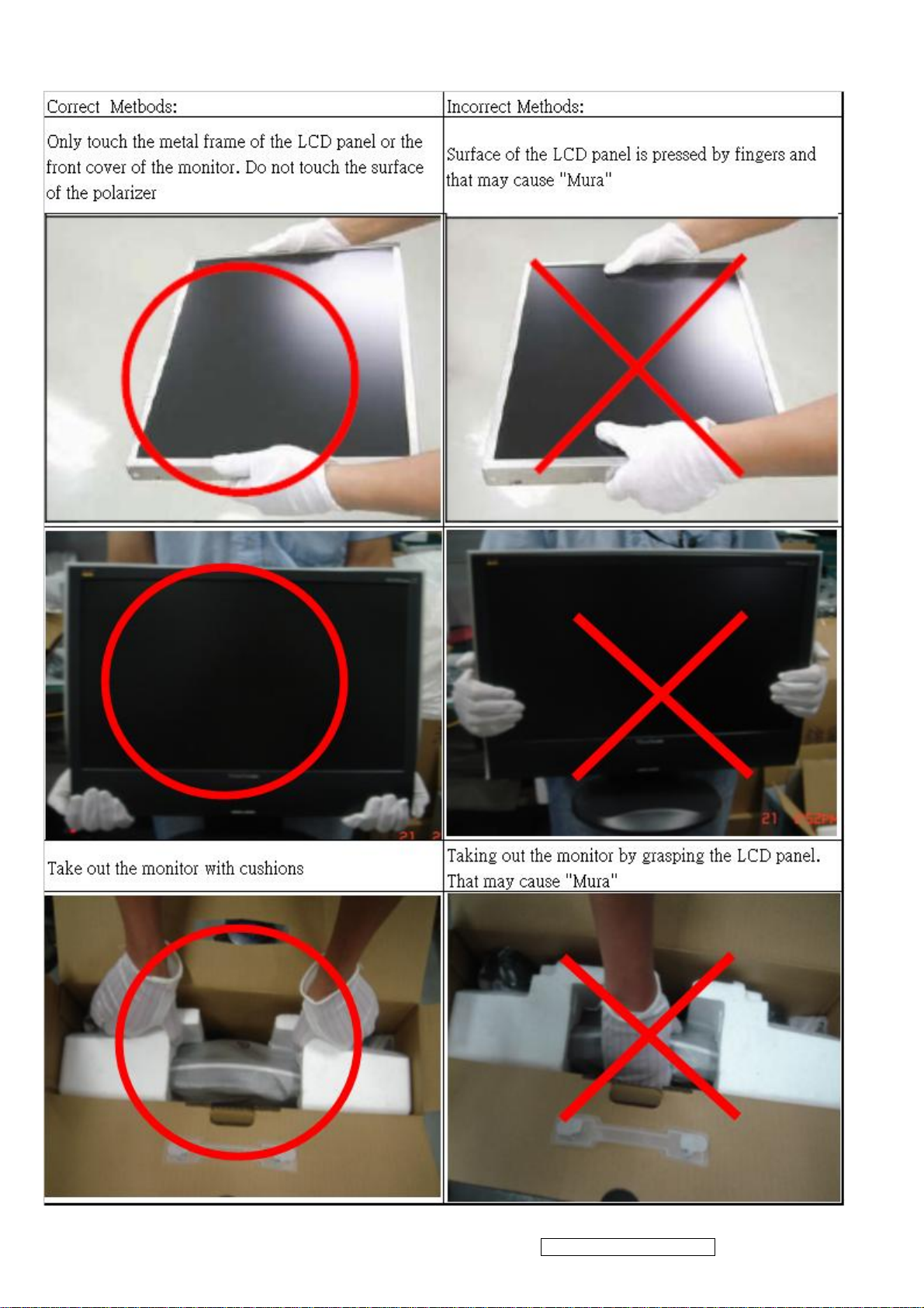
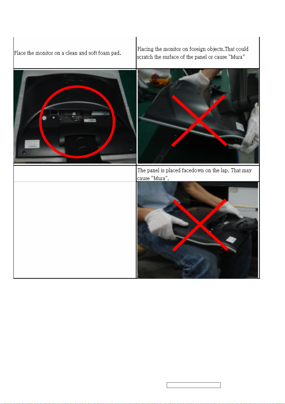
4. Handling and Placing Methods
ViewSonic Corporation Confidential - Do Not Copy VG1921wm-2
2
Page 6
ViewSonic Corporation Confidential - Do Not Copy VG1921wm-2
3
Page 7
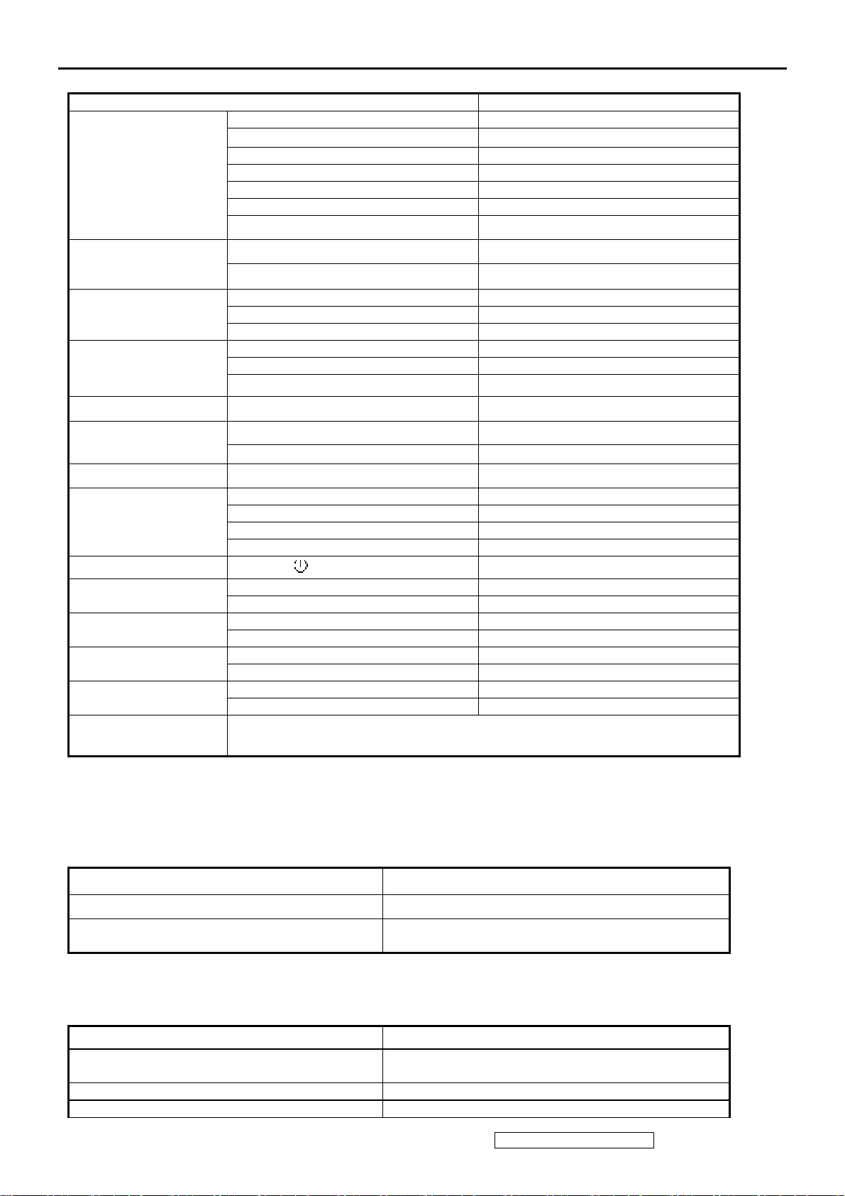
2. Specification
1. INTPRODUCTION
FEATURES
Size 19 ”
Luminance (Typ)
Contrast Ratio (Typ) 700:1
TFTLCD PANEL
Input Signal
Sync Compatibility
Compatibility
Power Voltage AC 100-240V, 50/60Hz Yes
Colors (6 bits + 2 bits FRC) 16.2 M
Response Time (Typ) 5 ms
Viewing Angle (H/V) 160 ° / 160 °
Recommend resolution 1440x900@60Hz
Analog (75ohms, 0.7/1.0 Vp-p) Yes
Digital No
Separate Sync Yes
Composite Sync Yes
Sync on Green Yes
PC Yes
Power Mac Yes
TV Box (NextVision 6) Yes
VG1921wm
300 cd/㎡
Power Consumption
Audio Yes
Ergonomics
OSD Control [ 1 ] [ 2 ] [ ][▼] [▲] Yes
Dimension
Weight
Operating Condition
Storage Condition
Regulation
On Mode(Max / Typ) 42 W
Off Mode (Max)
Tilt ( 20 ° - -5 °) Yes
Swivel No
Pivot No
Height Adjust No
Physical (W x H x D) 460 x 434 x 230 mm
Package (W x H x D) 560 x 525 x 282 mm
Physical (Net Weight) 5.4 kg
Package (Gross Weight) 6.9 kg
Temperature ( / )℉℃ 32℉-104 / ℉ 0℃-40℃
Humidity (%) 10 % - 90 %
Temperature ( / )℉℃ -4℉-140 / ℉ -20℃-60℃
Humidity (%) 10% - 90 %
UL, CUL, FCC-B (ICES), CB, CE, TCO'03, ICES-003B, ISO13406-2, TUV/GS, TUV ERGO(covers
ISO13406-2 & MPRII), TUV-S, NOM, GOST-R, HYGIENIC (20 copies), ENERGY, Energy Star,
CCC, BSMI, PSB, C-TICK, KTL/MIC, SASO, WEEE, RoHS
≦1 W
2 GENERAL specification
Test Resolution & Frequency 1440x900 @ 60Hz
Test Image Size Full Size
Contrast and Brightness Controls
Factory Default:
Contrast = 70%, Brightness = 100%
3 VIDEO INTERFACE
Analog Input Connector DB-15 (Analog), refer the appendix A
Video Cable Strain Relief
Video Cable Connector DB-15 Pin out Compliant DDC 1/2B
Video Signals Video RGB (Analog) – Separate,
ViewSonic Corporation Confidential - Do Not Copy VG1921wm-2
4
Equal to twice the weight of the monitor for five
minutes
Page 8
Video Impedance 75 Ohms (Analog)
Maximum PC Video Signal 950 mV with no damage to monitor
Maximum Mac Video Signal 1250 mV with no damage to monitor
DDC 1/2B Compliant with Revision 1.3
Sync Compatibility Separate Sync
Video Compatibility
Resolution Compatibility
Exclusions Not compatible with interlaced video
Shall be compatible with all PC type computers,
Macintosh computers, and after market video cards
640 x 350, 640 x 480, 720 x 400 (640 x 400*), 800 x
600, 832 x 624, 1024 x 768, 1152 x 864, 1280 x 960,
1280 x 1024,1440x900
4 POWER SUPPLY
Internal Power Supply Part Number:RLPR-025
Input Voltage Range 90 to 264 VAC
Input Frequency Range 47 to 63 Hertz
Short Circuit Protection OUTPUT CAN BE SHORTED WITHOUT DAMAGE
Over Current Protection 4 A TYPICAL AT 14.2 VDC
Leakage Current 3.5MA (MAX) AT 254VAC / 60HZ
Efficiency 80% TYPICAL AT 115VAC FULL LOAD
Fuse INTERNAL AND NOT USER REPLACEABLE
Power Dissipation 32 WATTS (TYP)
Max Input AC Current 0.8 ARMS @ 90VAC, 0.4 ARMS @265VAC
Inrush Current (Cold Start) 40 A @ 120VAC, 60 A (MAX) @ 220VAC
SHALL START AND FUNCTION PROPERLY WHEN
Power Supply Cold Start
Power Supply Transient Immunity
Power Supply Line Surge Immunity
Power Supply Missing Cycle Immunity
Power Supply Acoustics
US Type Power Cable
European Type Power Cable
CCC Type Power Cable
PSE Type Power Cable
Power Saving Operation(Method)
Power Consumption
Recovery Time On Mode = N/A, Active Off < 3 sec
ViewSonic Corporation Confidential - Do Not Copy VG1921wm-2
5
UNDER FULL LOAD, WITH ALL COMBINATIONS
OF INPUT VOLTAGE, INPUT FREQUENCY, AND
OPERATING TEMPERATURE
SHALL BE ABLE TO WITHSTAND AN ANSI/IEEE
C62.41-1980 2000V 200 AMPERE RING WAVE
TRANSIENT TEST WITH NO DAMAGE
Shall be able to withstand 1.5 times nominal line
voltage for one cycle with no damage
Shall be able to function properly, without reset or
visible screen artifacts, when ½ cycle of AC power is
randomly missing at nominal input
The power supply shall not produce audible noise
that would be detectable by the user. Audible shall
be defined to be in compliance with ISO 7779 (DIN
EN27779:1991) Noise measurements of machines
acoustics. Power Switch noise shall not be
considered
Separate 3-prong NEMA 5-15P type plug. Length =
1.8m. Connects to display.
Color = Black
Schuko CEE7-7 type plug.
Length = 1.8m, Connects to display.
Color = Black
Separate 3-prong type plug.
Length = 1.8m. Connects to display.
Color = Black
Separate 2-prong NEMA 1-15P type plug. Length =
1.8m. Connects to display.
Color = Black
VESA DPMS Signaling
On Mode <42 W (max)
Off Mode< 1W
Page 9
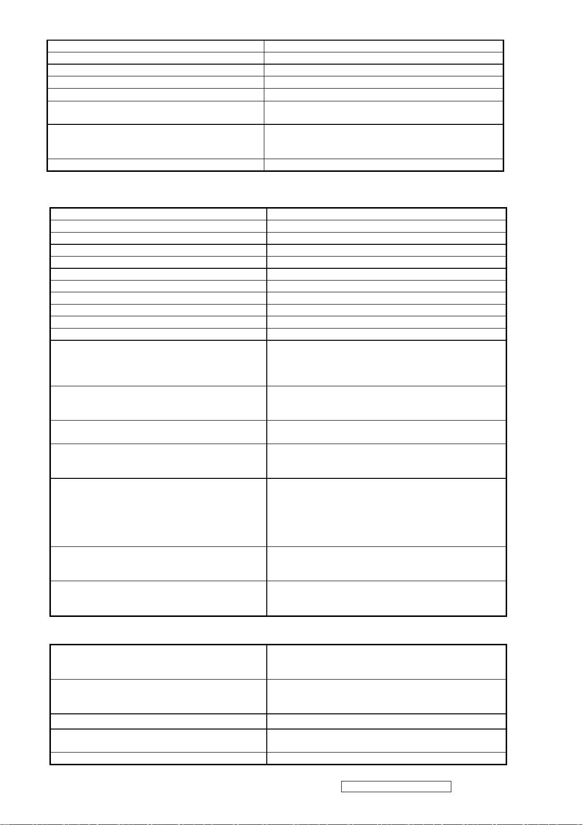
5 ELECTRICAL REQUIREMENT
Horizontal / Vertical Frequency
Horizontal Frequency 30 – 82 kHz
Vertical Refresh Rate
Maximum Pixel Clock 135 MHz
Sync Polarity Independent of sync polarity.
Timing Table
Item Timing
50 – 75* Hz.
Analog
Composite
Separated
SOG
Digital - TMDS
Remark
640 x 350 @ 70 Hz, 31.5 KHz
1
640 x 400 @ 60 Hz, 31.5 KHz
2
640 x 400 @ 70 Hz, 31.5 KHz
3
640 x 480 @ 50 Hz, 24.7 KHz
4
640 x 480 @ 60 Hz, 31.5 KHz
5
640 x 480 @ 67 Hz, 35 KHz
6
640 x 480 @ 72 Hz, 37.9 KHz
7
640 x 480 @ 75 Hz, 37.5 KHz
8
720 x 400 @ 70 Hz, 31.5 KHz
9
10
11
12
13
14
15
16
17
18
19
20
21
720 x 480 @ 60 Hz, 31.5 KHz
720 x 576 @ 50 Hz, 31.3 KHz
800 x 600 @ 56 Hz, 35.1 KHz
800 x 600 @ 60 Hz, 37.9 KHz
800 x 600 @ 72 Hz, 48.1 KHz
800 x 600 @ 75 Hz, 46.9 KHz
832 x 624 @ 75 Hz, 49.7 KHz
1024 x 768 @ 50 Hz, 39.6 KHz
1024 x 768 @ 60 Hz, 48.4 KHz
1024 x 768 @ 70 Hz, 56.5 KHz
1024 x 768 @ 72 Hz, 58.1 KHz
1024 x 768 @ 75 Hz, 60 KHz
1024 x 768 @ 75 Hz, 60.2 KHz
22
DMT
DMT
For MAC
DMT
DMT
DTV
DTV
DMT
DMT
DMT
DMT
MAC
DMT
DMT
DMT
For MAC
1152 x 864 @ 75 Hz, 67.5 KHz
23
1152 x 870 @ 75 Hz, 68.7 KHz
24
1152 x 900 @ 67 Hz, 62.5 KHz
25
1280 x 720 @ 50 Hz, 37.5 KHz
26
1280 x 720 @ 60 Hz, 45 KHz
27
1280 x 768 @ 50 Hz, 39.6 KHz
28
DMT
For MAC
For SUN
DTV
DTV
ViewSonic Corporation Confidential - Do Not Copy VG1921wm-2
6
Page 10
1280 x 768 @ 60 Hz, 47.8 KHz
29
1280 x 768 @ 75 Hz, 60.3 KHz
30
1280 x 960 @ 50 Hz, 49.4 KHz
31
1280 x 960 @ 60 Hz, 59.7 KHz
32
1280 x 960 @ 75 Hz, 75.2 KHz
33
1280 x 1024 @ 50 Hz, 52.7 KHz
34
1280 x 1024 @ 60 Hz, 64 KHz
35
1280 x 1024 @ 75 Hz, 80 KHz
36
1440 x 900 @ 60 Hz 59.9 KHz
37
DMT;
DMT;
DMT
DMT
DMT
DMT
Primary Presets
1440x900 @ 60Hz
User Presets
Number of User Presets (recognized timings) Available: 10 presets total in FIFO configuration
Changing Modes
● Maximum Mode Change Blank Time for image stability: 3 seconds (Max), excluding “Auto Image Adjust” time.
● Under DOS mode (640 x 350, 720 x 400 & 640 x 400), it should recall factory setting when execute “Auto Image
Adjust”.
The monitor needs to do “Auto Image Adjust” the first time when a new mode is detected. (See section “0-Touch™
Function Actions”)
6 FRONT PANEL CONTROLS AND INDICATORS
Front Panel Hardware Controls
Power Switch (Front Head) Power Control, soft Power Switch.
Green – ON
Power LED (Front Head)
Front Panel Controls (Head)
] [ 1 ] [ 2 ] [▲] [▼]
[
Reaction Time
Short Cuts Function from the button(s)
[1] Main Menu
[2] Input toggle (Analog or Digital; refer to Appendix D)
[▼] Brightness adjust
[▲] Contrast adjust
[▼]+ [▲] recall both of Contrast and Brightness to default
[1] + [2] toggle 720x400 and 640x400 mode when input 720x400 or 640x400
mode
[1] + [▼] + [▲] White Balance. (Not shown on user’s guide)
[1] + [▼] Power Lock
[1] + [▲] OSD Lock
[1] + [▼] + [2] Disable Theft Defence function
[▲]+ [ ] + Main Power On All reset
No signal + [ ] + [2]
+ Main Power on
Burning mode
Orange – Active Off
Dark = Soft Power Switch OFF
[;X] Mute
] Power
[
[ 1 ] Button 1
[ 2 ] Button 2
[▲] Up arrow button
[▼] Down arrow button
Note: Power Button, Button 1 and Button 2 must be
one-shot logic operation. (i.e. there should be no
cycling)
OSD must fully appear within 0.5s after pushing Button
1
ViewSonic Corporation Confidential - Do Not Copy VG1921wm-2
7
Page 11
Signal + [2] + [
] + Main Power
On
Factory Mode
Remark : All the short cuts function are only available while OSD off
Main Menu Controls
The Main Menu OSD includes most of control functions.
Please refer to APPENDIX C (Main Menu OSD Table) for the detail.
Function descriptions
OSD Lock short cuts function for the buttons
The OSD lock will be activated by pressing the front panel control buttons "(1), & (▲)" for 10 seconds. If
the user then tries to access the OSD by pressing any of the buttons "1", "▼", "▲", "2" a message will
appear on the screen for 3 seconds showing "OSD Locked". The OSD lock will be deactivated by
pressing the front panel control buttons "(1), & (▲)" again for 10 seconds.
Note1: When the OSD is locked will lock all functions, including “Volume” and “Mute”
Note 2: Status bar indicating OSD Lock or Unlock is in progress and when complete it will indicate “OSD
Locked”
Note 3: OSD Lock should not lock Power Button and Power Lock function
Power Lock short cuts function for the buttons
The power button lock will be activated by pressing the front panel control buttons "(1), & (▼)" for 10
seconds. Locking the power button means that the user won't be able to turn off the LCD while the power
button is locked. If the user presses the power button while it is locked, a message will appear on the
screen for 3 seconds showing "Power Button Locked". It also means that with the power button locked,
the LCD would automatically turn back "On" when power is restored after a power failure. If the power
button is not in the locked mode, then power should return to it's previous state when power is restored
after a power failure. The power button lock will be deactivated by pressing the front panel control buttons
"(1), & (▼)" again for 10 seconds.
Note 1: Status bar indicating Power Button lock or unlock is in progress and when complete it will
indicate “Power Button Locked”
Note 2: Power should only be lockable in the “On State”
Memory Recall Actions
Memory Recall action on the analog and digital mode as below
1. Recall white balance to factory setting
2. Set the factory defaults as shown in Section 4-8
3. Clean all the mode setting buffer
4. Execute Auto Image Adjust
Note: Memory Recall should have no effect for Language, Power Lock, User Color Settings or Input
Priority
Resolution Notice Actions
1. Resolution Notice OSD should show on screen after changing to non-native mode for 30 sec
2. For auto input select function, it shall meet the requirement in Appendix D.
3. The OSD should disappear after 10 sec or by pushing button [1] or [2]
Resolution Notice function should be disabled when push button [2] under Resolution Notice OSD
0-Touch™ Function Actions
1. Execute Auto Image Adjust when new mode detected, and save the settings to buffer for further use
2. It should be reset by Memory Recall function(Should not reset by power off, power unplug and others)
OSD Auto Save
The OSD shall save new settings when it is turned off by the user or when it times out. There shall not
be a separate save
ViewSonic Corporation Confidential - Do Not Copy VG1921wm-2
8
Page 12
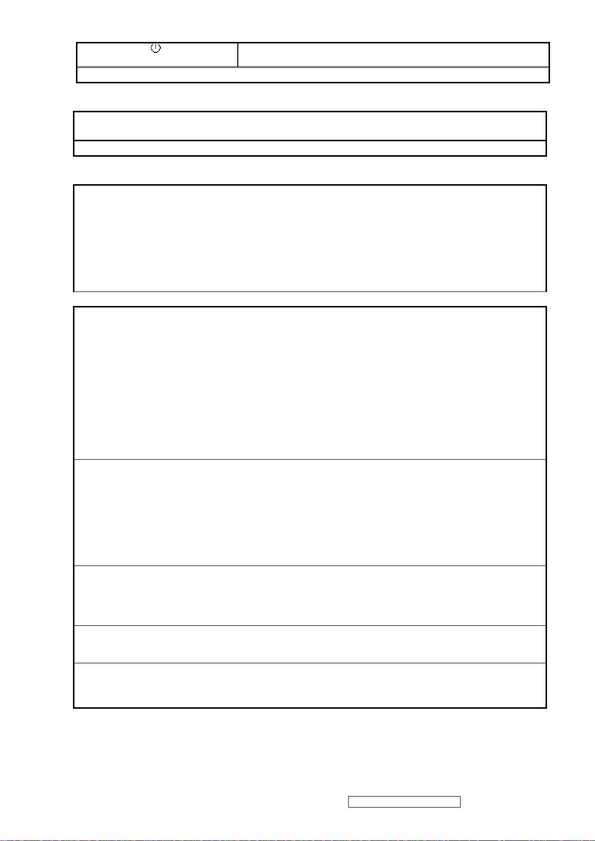
3. Front Panel Function Control Description
Adjusting the Screen Image
Use the buttons on the front control panel to display and adjust the OSD controls which display
on the screen. The OSD controls are explained at the top of the next page and are defined in
“Main Menu Controls” on page 10.
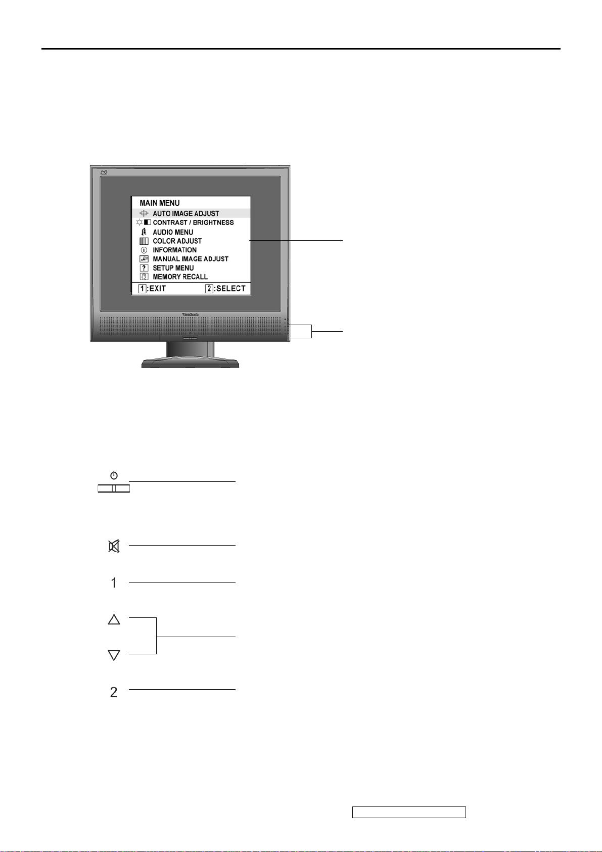
Main Menu
with OSD controls
Front Control Panel
shown below in detail
Standby Power On/Off
Power light
Blue = ON
Orange = Power Saving
Audio Mute button turns the sound off
Displays the Main Menu or exits the control screen and saves
adjustments.
Scrolls through menu options and adjusts the displayed control.
Also a shortcut to display the Contrast adjustment control screen.
Displays the control screen for the highlighted control.
Also toggles between two controls on some screens.
ViewSonic Corporation Confidential - Do Not Copy VG1921wm-2
9
Page 13
Do the following to adjust the display setting:
1. To display the Main Menu, press button [1].
NOTE: All OSD menus and adjustment screens disappear automatically after about 15
seconds. This is adjustable through the OSD timeout setting in the setup menu.
2. To select a control to adjust, pressSorTto scroll up or down in the Main Menu.
3. After the desired control is selected, press button [2]. A control screen like the one shown
below appears.
The command line at the bottom of the
control screen tells what to do next from
this screen. You can toggle between control
screens, adjust the selected option, or exit
the screen.
4. To adjust the setting, press the up S or down T buttons.
5. To save the adjustments and exit the menu, press button [1] twice.
The following tips may help you optimize your display:
• Adjust the computer's graphics card so that it outputs a 1440 x 900 @ 60Hz video signal to
the LCD display. (Look for instructions on “changing the refresh rate” in the graphics card's
user guide.)
• If necessary, make small adjustments using H. POSITION and V. POSITION until the
screen image is completely visible
. (The black border around the edge of the screen should
barely touch the illuminated “active area” of the LCD display.)
ViewSonic Corporation Confidential - Do Not Copy VG1921wm-2
10
Page 14
Main Menu Controls
Adjust the menu items shown below by using the up S and down T buttons.
Control Explanation
Auto Image Adjust sizes and centers the screen image automatically.
Contrast adjusts the difference between the image background (black level)
and the foreground (white level).
Brightness adjusts background black level of the screen image.
Audio Adjust
Vol ume increases the volume, decreases the volume, and mutes the audio.
Mute temporarily silences audio output.
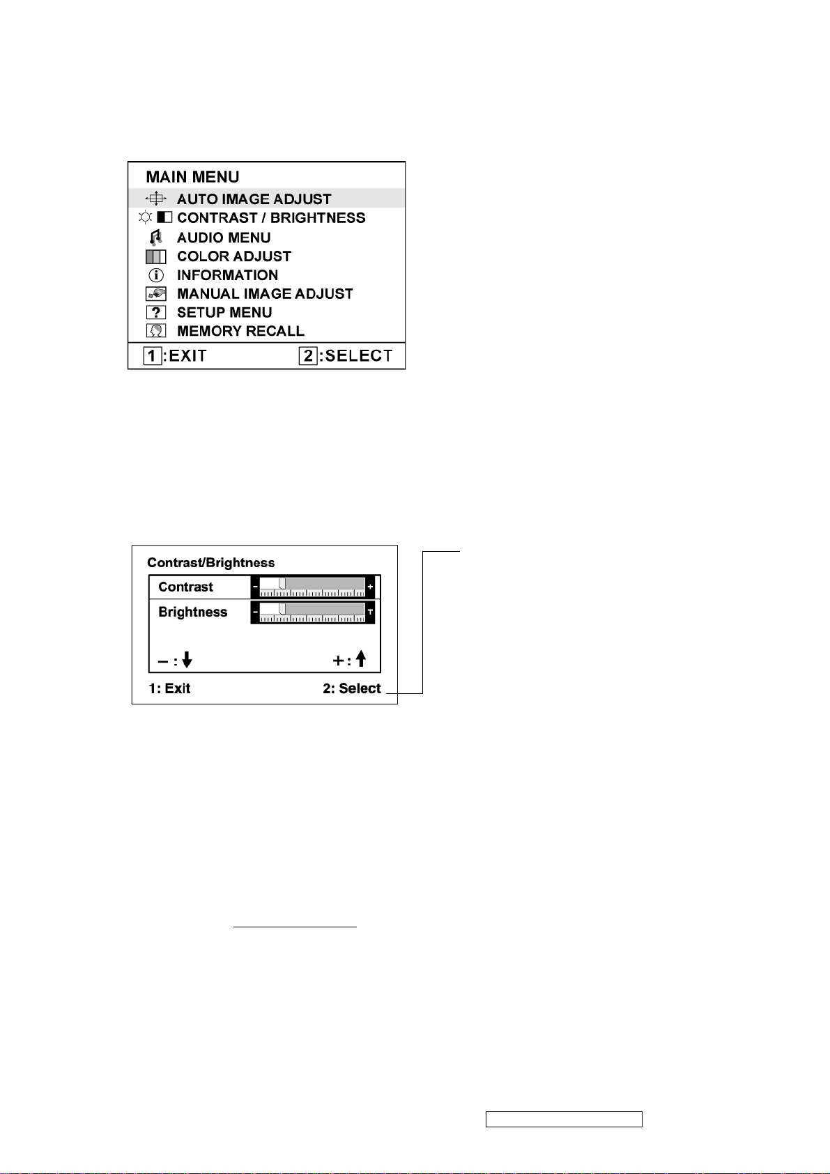
Color Adjust provides several color adjustment modes, including preset color
temperatures and a User Color mode which allows independent adjustment of
red (R), green (G), and blue (B). The factory setting for this product is 6500K
(6500 Kelvin).
sRGB-This is quickly becoming the industry standard for color management,
with support being included in many of the latest applications. Enabling this
setting allows the LCD display to more accurately display colors the way they
were originally intended. Enabling the sRGB setting will cause the Contrast and
Brightness adjustments to be disabled.
9300K-Adds blue to the screen image for cooler white (used in most office
settings with fluorescent lighting).
7500K-Adds blue to the screen image for cooler white (used in most office
settings with fluorescent lighting).
6500K-Adds red to the screen image for warmer white and richer red.
5400K-Adds green to the screen image for a darker color.
ViewSonic Corporation Confidential - Do Not Copy VG1921wm-2
11
Page 15
Control Explanation
User Color Individual adjustments for red (R), green (G), and blue (B).
1. To select color (R, G or B) press button [2].
2. To adjust selected color, pressSandT.
Important: If you select RECALL from the Main Menu when the product is
set to a Preset Timing Mode, colors return to the 6500K factory preset.
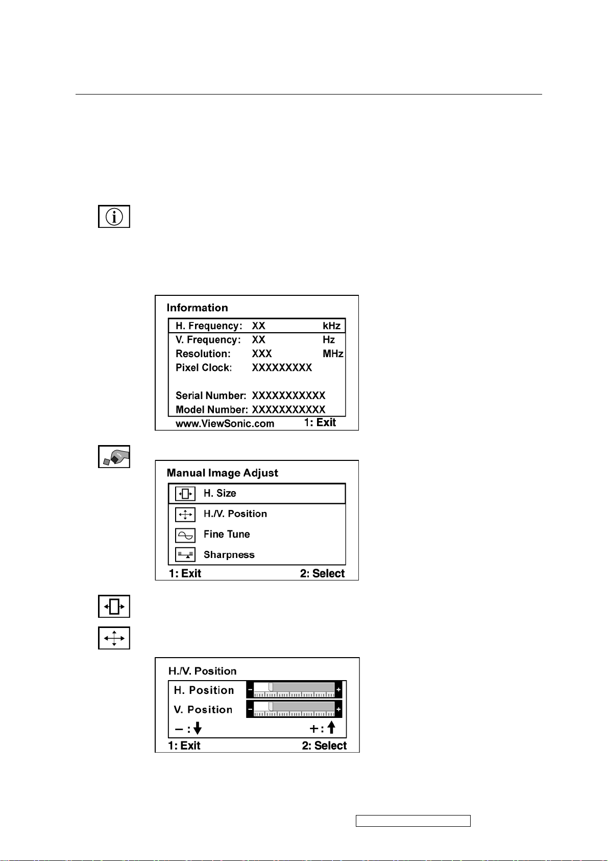
Information displays the timing mode (video signal input) coming from the
graphics card in the computer, the LCD model number, the serial number, and
the ViewSonic® website URL. See your graphics card’s user guide for
instructions on changing the resolution and refresh rate (vertical frequency).
NOTE: VESA 1440 x 900 @ 60Hz (recommended) means that the resolution is
1440 x 900 and the refresh rate is 60 Hertz.
Manual Image Adjust
H. Size (Horizontal Size) adjusts the width of the screen image.
H./V. Position (Horizontal/Vertical Position) moves the screen image left or
right and up or down.
ViewSonic Corporation Confidential - Do Not Copy VG1921wm-2
12
Page 16
Control Explanation
Fine Tune sharpens the focus by aligning text and/or graphics with pixel
boundaries.
NOTE: Try Auto Image Adjust first.
Sharpness adjusts the clarity and focus of the screen image.
Setup Menu displays the menu shown below:
Language Select allows the user to choose the language used in the menus and
control screens.
Resolution Notice allows the user to enable or disable this notice.
If you enable the Resolution Notice shown above and your computer is set at a
resolution other than 1440 x 900, the following screen appears.
OSD Position allows the user to move the OSD menus and control screens.
OSD Timeout sets the length of time the OSD screen is displayed. For example,
with a “30 second” setting, if a control is not pushed within 30 seconds, the
display screen disappears.
ViewSonic Corporation Confidential - Do Not Copy VG1921wm-2
13
Page 17

4. Circuit Description
4.1 Switching Mode Power Supply
4.1.1 AC Current Input Circuit
P801 is a connector for connecting AC Power. F801 is a fuse to protect all the circuit. AC
input voltage is from 90v to 264V. R801 and R802 joined between two inputting main circuit to
prevent man from shock. L801 is used to clear up low frequency wave. C801 and C802 are used
to discharge the waves that L801 produced. High frequency waves are damped by C801 and
C802. D801 is a rectifier which composed of 4 build-in diodes, it inverts AC to DC.
4.1.2 High Voltage to Low Voltage Control Circuit
C804 is used to smooth the wave from rectifier. IC802 is a highly integrated PWM controller.
When rectified DC high voltage is applied to the HV pin during start-up, the MOSFET Q804 is
initially off, and the Vcc pin capacitor is charged. When the Vcc pin voltage reaches
approximately 10V, the control circuitry is activated and the soft-start begins. The soft-start
circuit gradually increases the duty cycle of the MOSFET from zero to the maximum value
over approximately 4ms. If no external feedback/supply current is fed into the FB pin by the
end of the soft-start, the current Setpoint will be above the fault level, FAULT flag is raised, if
the FAULT duration exceeds 80ms, the output controller disable
Resistor R808, R809, R810, R811 are for line over voltage shutdown(OVP)
When PWM is turned off, the main current flow will be consumed through R804 and
D802, This will prevent MOSFET Q804 from being damaged under large current impulse
and voltage spike.
D803 and C807 to provide internal Auxiliary voltage to Vcc pin during normal operation.
Otherwise, error amplifier and feedback current input the FB pin for duty cycle control.
4.1.3 DC_5V and DC_14V Output Circuit
For DC 5V, D805 is used to rectify the inducted current. R828 and C814 are used to store
energy when current is reversed. The parts including C818, C822, C820,L803 are used to
smooth the current waves.
For DC 14V, D803 is used to rectify the inducted current. R827 and C813 are used to
store energy when current is reversed. The parts including C815, C817 and L802 are used to
smooth the current waves.
4.1.4 Feedback and OVP Protect Circuit
Pin R of IC803 is supplied 2.5-v stable voltage. It connects to 5V and 14V output through
R822, R823 and R824. R822, R823 and R824 are output sampling resistor. When the sampling
voltage more than 2.5V or less than 2.5V, current of FB IC802 will change, this can change the
voltage from T801.
OVP Protect Circuit: When output is overvoltage, the auxiliary winding voltage will be
increased, when it reaches about 14V. Q803 is triggered . It makes the IC802 Pin 1 exceed 5V,
then the IC802 output will be disabled.
Q801, R816, R817 and ZD803 make up of dummy loading circuit. For start-up sequence,
during 5V output take place high loading first, this dummy loading circuit operated to insure
14V not be increased.
4. 2 Inverter Circuit
1R503, ZD501, R502, Q501 components convert +14V voltage into +5.0V voltage, and the voltage supply to
IC501. The extra PWM pulse signal (BRIGHTNESS signal)input to control IC through R512, R514, C510, The
LCT pin is set to a DC voltage of 0.7V by using a resistor divider(R507, R516), change the duty of PWM pulse,
will regulate the lamp current. The ON/OFF voltage connect to pin10 of IC501 through D501, R501, A voltage of
ViewSonic Corporation Confidential - Do Not Copy VG1921wm-2
14
Page 18

2V to pin10 of IC501 enables the IC and activates the striking timer. The SSTCMP pin of IC501 performs the soft
function, the C511 set the time of SST. The operation frequency determined by external capacitor C512, C521 and
resistor R508 connected at CT pin of IC501. C515 connect the TIMER pin of IC501, the capacitor to set striking
time and shunt down delay time. DRV!, DRV2 output for power MOSFET U501, U502.
2.OZ9938 provides two drive signals forU501, U502, and they work in push pull topology driving, two
transformers are connected in parallel with each transformer driving two lamps in series.Turningeach N-Channel
MOSFET “on/off" complementarily, produces an alternating current through thetransformer primary and
secondary. The “on" duration of the switches determines the amount of energy delivered to the CCFLs. R504,
C504, R505, C505, R532, C529, R530, C522 are snubber networks, they suppress Voltage transient spike in drain
of power MOSFET.
3. R506, R510, C509, C513, C514, R525, R531, C528, C525, and C527 are connected betweenhigh voltage
output connector and ground, the divided AC voltage is inverted DC voltage through D502, D503, D508, and
D509.The sense voltage feedback to VSEN (pin 6 of IC501) for an over voltage/over current condition during
normal operation. R528, R533 are current sense resistor, current sense signal feed back to Isense (pin 5 of IC501)
for lamp “ON" detection.
4.3 I/F Board Circuit
4.2.1 Power Input
+5V is from the power board and supply for U101(LD1117AL-3.3V)、U105(TSUM56AL-1) and panel.
+3.3V output is generated from +5V through C101 and C103 filtering, and U101 outputs. +3.3V is used
for U105 (MCU & Scaler: TSUM16AL). +1.8V output is generated from +3.3V through U102 outputs.
+1.8V is only used for U105.
4.2.2 MCU & Scaler(TSUM16AL)
The frequency of XTAL1 is 14.318MHz. U105 # 48 is defined as panel-enable. When the I/O port is
high, Q101 and Q103 are conducted. And then after C108 and C109 filtering, obtain the voltage of VLCD,
which will be connected to CN104. U105 # 85 is defined as CCFL-enable. When the I/O port is low, Q106
is pulled up and the backlights are on; When the I/O port is high, Q106 is conducted and the backlights
are off. U105 # 35 is defined as DET-VGA, connected with CN103 #5. U105 # 84 is a pin of hardware
reset. U105 # 54-# 55,# 58-# 65, # 67-# 74, # 77-# 78 output LVDS digital data of 8 bit to panel control
circuit through CN104. U105 # 86 generates a PWM waveform by regulating the duty to control the
brightness of the backlights.
U103 is EEPROM used for saving EDID data, which is connected by SCL and SDA pins with # 31 and
# 30 of TSUM56AL-1.
U106 is a flash memory, U106 # 2, # 1, # 6, # 5 are the communications with U105 # 37-# 40.
U108 is EEPROM used for saving user’s OSD setting. U108 is connected by SCL and SDA pin with # 44
and # 43 of TSUM16AL.
4.2.3 VGA Input
Signal R, G, B input through CN103 #1, #2, #3, and C112, C113 and C114 filtering the high frequency
noise. Signal HSYNC and VSYNC input through CN103 #13 and #14, and C125, R137, C126, R136
filtering. Then the analog signal enters U105, and then U104 deals with it internally. In addition, TVS101,
TVS102, TVS103, TVS104 (the four are BAV99), ZD101, ZD105, ZD106, ZD107, ZD108(they are
constant voltage diode of 5V6) are ESD protector. Signal DDC-SCL inputs via CN103 #15, and then
passes through ZD101 for ESD protection, goes into EDID EEPROM IC U103. Signal DDC-SDA inputs
via CN103 #12, and then passes through ZD107 for ESD protection, goes into EDID EEPROM IC U103.
CN103 #5 is defined as cable detect pin, this detector realizes via R124 and U105 # 35,The PC-5V of
U103 is supplied by PC via CN103 #9 with D103 for ESD protection, or supplied by Monitor self via
D103.U103 is an EEPROM IC, which is a kind of memory and used for saving EDID data.
4.2.4 Button Control
Button “Key-Power” is defined as power on/off, which is connected to U105 # 90 through CN105 # 6.
Button “Key-2” is defined as two functions of selecting and adjustment, which is connected to U105 #94
through CN105 # 5.
Button “Key-Up” is defined as plus, which is connected to U105 # 95 through CN105 # 8.
Button “Key-Down” is defined as minus, which is connected to U105 # 99 through CN105 # 7.
Button “Key-1” is defined as two functions of menu and exit, which is connected to U105 # 89 through
CN105 # 4.
LED indicator on the front bezel is defined as follows:
a. When press button “Key-Power”, U105 # 91 is pulled down and U105 # 92 is pulled high, so Q102 is
conducted and the LED indicator is green.
ViewSonic Corporation Confidential - Do Not Copy VG1921wm-2
15
Page 19
b. When in power-saving mode, U105 # 91 is pulled high and U105 # 92 is pulled down, so Q105 is
conducted and the LED indicator is orange.
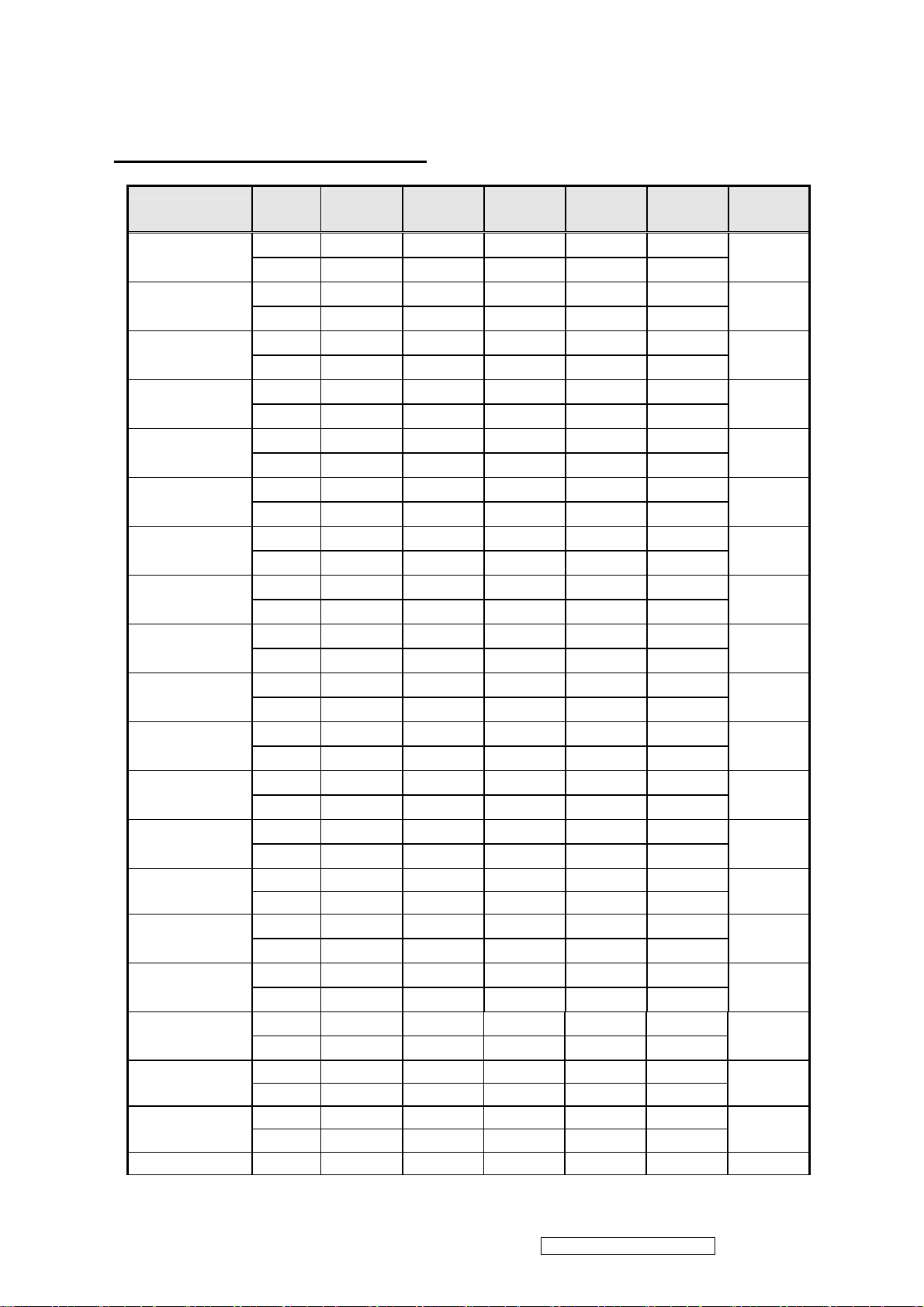
4.4 FACTORY PRESET TIMING TABLE
TIMING
FH(KHz)
FV(Hz)
Sync
Polarity
Total
(Dot/Line)
Active
(Dot/Line)
Sync Width
(Dot/Line)
Back Porch
(Dot/Line)
Pixel
Freq.(MHz)
640*350@70Hz
IBM
640*400@70Hz
IBM
720*400@70Hz
640*480@50Hz
VESA
640*480@60Hz
640*480@67Hz
VESA
640*480@72Hz
VESA
640*480@75Hz
VESA
640*480@85Hz
VESA
800*600@56Hz
VESA
800*600@60Hz
VESA
800*600@72Hz
VESA
800*600@75Hz
VESA
800*600@85Hz
MAC
832*624@75Hz
VESA
1024*768@60Hz
VESA
1024*768@70Hz
1024*768@75Hz
1024*768@85Hz
1024*768@72Hz 57.700 − 1360 1024 136 144 78.472
31.469 + 800 640 96 48
70.086 − 449 350 2 60
31.469 − 800 640 96 48
70.086 + 449 400 2 35
31.469 −
70.087 +
24.700 −
50.000 −
31.469 −
59.940 −
35.000 −
66.667 −
37.861 −
72.809 −
37.500 −
75.000 −
43.269 −
85.008 −
35.156 +
56.250 +
37.879 +
60.317 +
48.077 +
72.188 +
46.875 +
75.000 +
53.674 + 1048 800 64 152
85.061 + 631 600 3 27
49.725 −
74.550 −
48.363
60.004
56.476
70.069
60.023 + 1312 1024 96 176 VESA
75.029 + 800 768 3 28
68.677 + 1376 1024 96 208 VESA
84.997 + 808 768 3 36
−
−
−
−
900 720 108 54
449 400 2 35
800 640 96 48
494 480 2 8
800 640 96 40
525 480 2 25
864 640 64 96
525 480 3 39
832 640 40 120
520 480 3 20
840 640 64 120
500 480 3 16
832 640 56 80
509 480 3 25
1024 800 72 128
625 600 2 22
1056 800 128 88
628 600 4 23
1040 800 120 64
666 600 6 23
1056 800 80 160
625 600 3 21
1152 832 64 224
667 632 3 39
1344 1024
806 768
1328 1024 136 144
806 768 6 29
136 160
6 29
75.000
78.750
94.500
25.175
25.175
28.322
19.760
25.175
30.240
31.500
31.500
36.000
36.000
40.000
50.000
49.500
56.250
57.283
65.000
ViewSonic Corporation Confidential - Do Not Copy VG1921wm-2
16
Page 20

2V to pin10 of IC501 enables the IC and activates the striking timer. The SSTCMP pin of IC501 performs the soft
function, the C511 set the time of SST. The operation frequency determined by external capacitor C512, C521 and
resistor R508 connected at CT pin of IC501. C515 connect the TIMER pin of IC501, the capacitor to set striking
time and shunt down delay time. DRV!, DRV2 output for power MOSFET U501, U502.
2.OZ9938 provides two drive signals forU501, U502, and they work in push pull topology driving, two
transformers are connected in parallel with each transformer driving two lamps in series.Turningeach N-Channel
MOSFET “on/off" complementarily, produces an alternating current through thetransformer primary and
secondary. The “on" duration of the switches determines the amount of energy delivered to the CCFLs. R504,
C504, R505, C505, R532, C529, R530, C522 are snubber networks, they suppress Voltage transient spike in drain
of power MOSFET.
3. R506, R510, C509, C513, C514, R525, R531, C528, C525, and C527 are connected betweenhigh voltage
output connector and ground, the divided AC voltage is inverted DC voltage through D502, D503, D508, and
D509.The sense voltage feedback to VSEN (pin 6 of IC501) for an over voltage/over current condition during
normal operation. R528, R533 are current sense resistor, current sense signal feed back to Isense (pin 5 of IC501)
for lamp “ON" detection.
4.3 I/F Board Circuit
4.2.1 Power Input
+5V is from the power board and supply for U101(LD1117AL-3.3V)、U105(TSUM56AL-1) and panel.
+3.3V output is generated from +5V through C101 and C103 filtering, and U101 outputs. +3.3V is used
for U105 (MCU & Scaler: TSUM16AL). +1.8V output is generated from +3.3V through U102 outputs.
+1.8V is only used for U105.
4.2.2 MCU & Scaler(TSUM16AL)
The frequency of XTAL1 is 14.318MHz. U105 # 48 is defined as panel-enable. When the I/O port is
high, Q101 and Q103 are conducted. And then after C108 and C109 filtering, obtain the voltage of VLCD,
which will be connected to CN104. U105 # 85 is defined as CCFL-enable. When the I/O port is low, Q106
is pulled up and the backlights are on; When the I/O port is high, Q106 is conducted and the backlights
are off. U105 # 35 is defined as DET-VGA, connected with CN103 #5. U105 # 84 is a pin of hardware
reset. U105 # 54-# 55,# 58-# 65, # 67-# 74, # 77-# 78 output LVDS digital data of 8 bit to panel control
circuit through CN104. U105 # 86 generates a PWM waveform by regulating the duty to control the
brightness of the backlights.
U103 is EEPROM used for saving EDID data, which is connected by SCL and SDA pins with # 31 and
# 30 of TSUM56AL-1.
U106 is a flash memory, U106 # 2, # 1, # 6, # 5 are the communications with U105 # 37-# 40.
U108 is EEPROM used for saving user’s OSD setting. U108 is connected by SCL and SDA pin with # 44
and # 43 of TSUM16AL.
4.2.3 VGA Input
Signal R, G, B input through CN103 #1, #2, #3, and C112, C113 and C114 filtering the high frequency
noise. Signal HSYNC and VSYNC input through CN103 #13 and #14, and C125, R137, C126, R136
filtering. Then the analog signal enters U105, and then U104 deals with it internally. In addition, TVS101,
TVS102, TVS103, TVS104 (the four are BAV99), ZD101, ZD105, ZD106, ZD107, ZD108(they are
constant voltage diode of 5V6) are ESD protector. Signal DDC-SCL inputs via CN103 #15, and then
passes through ZD101 for ESD protection, goes into EDID EEPROM IC U103. Signal DDC-SDA inputs
via CN103 #12, and then passes through ZD107 for ESD protection, goes into EDID EEPROM IC U103.
CN103 #5 is defined as cable detect pin, this detector realizes via R124 and U105 # 35,The PC-5V of
U103 is supplied by PC via CN103 #9 with D103 for ESD protection, or supplied by Monitor self via
D103.U103 is an EEPROM IC, which is a kind of memory and used for saving EDID data.
4.2.4 Button Control
Button “Key-Power” is defined as power on/off, which is connected to U105 # 90 through CN105 # 6.
Button “Key-2” is defined as two functions of selecting and adjustment, which is connected to U105 #94
through CN105 # 5.
Button “Key-Up” is defined as plus, which is connected to U105 # 95 through CN105 # 8.
Button “Key-Down” is defined as minus, which is connected to U105 # 99 through CN105 # 7.
Button “Key-1” is defined as two functions of menu and exit, which is connected to U105 # 89 through
CN105 # 4.
LED indicator on the front bezel is defined as follows:
a. When press button “Key-Power”, U105 # 91 is pulled down and U105 # 92 is pulled high, so Q102 is
conducted and the LED indicator is green.
ViewSonic Corporation Confidential - Do Not Copy VG1921wm-2
17
Page 21

4.6 AC Outlet Pin Assignment
Pin Symbol Description
3
1 2
1 L Live
2 N Neutral
P801
3 E GND
4.7 Inner Connector Pin Assignment
4.7.1 CN501, CN502, CN503, CN504 (Connect to Panel Backlight, SM02B-BHSS-1-TB or
equivalent
Pin Symbol Description
)
1 H.V. High voltage for lamp
2 L.V. Low voltage for lamp
4.7.2 CN101 (Power BD to Interface BD)
Pin No. Symbol Description
1 VCC5V +5.1V INPUT
2 VCC5V +5.1V INPUT
3 GND GND
4 ON/OFF CCFL on/off control
5 BRIGHTNESS Panel luminance control (CCFL brightness)
6 GND Ground
7 VOL Volume control input
8 MUTE Mute control input
4.7.3 CN105 (Interface BD to Keypad)
Pin
No.
1 LED_ GREEN Orange LED lighting control
2 LED_ ORANGE Green LED lighting control
3 GND Ground
4 KEY_POWER DC power on/off control,
KEY_UP&▲
5
6 KEY_DOWN&2 Select control and auto adjustment control,
7 GND OSD “▼” control to adjust value to decrease
8 KEY_1 OSD menu and exit
Symbol Description
OSD “▲” control to adjust value to increase,
ViewSonic Corporation Confidential - Do Not Copy VG1921wm-2
18
Page 22

4.7.4 CN104 (Connect I/F BD to panel, FI-X30S-H or Equivalent)
Pin No. Symbol Function
1 RXO0- minus signal of odd channel 0(LVDS)
2 RXO0+ plus signal of odd channel 0(LVDS)
3 RXO1- minus signal of odd channel 1(LVDS)
4 RXO1+ plus signal of odd channel 1(LVDS)
5 RXO2- minus signal of odd channel 2(LVDS)
6 RXO2+ plus signal of odd channel 2(LVDS)
7 GND Ground
8 RXOC- minus signal of odd clock channel (LVDS)
9 RXOC+ plus signal of odd clock channel (LVDS)
10 RXO3- minus signal of odd channel 3(LVDS)
11 RXO3+ plus signal of odd channel 3(LVDS)
12 RXE0- minus signal of even channel 0(LVDS)
13 RXE0+ plus signal of even channel 0(LVDS)
14 GND Ground
15 RXE1- minus signal of even channel 1(LVDS)
16 RXE1+ plus signal of even channel 1(LVDS)
17 GND Ground
18 RXE2- minus signal of even channel 2(LVDS)
19 RXE2+ plus signal of even channel 2(LVDS)
20 RXEC- minus signal of even clock channel (LVDS)
21 RXEC+ plus signal of even clock channel (LVDS)
22 RXE3- minus signal of even channel 3(LVDS)
23 RXE3+ plus signal of even channel 3(LVDS)
24 GND Ground
25
26
27
28 VCC Power supply (5.0 V)
29 VCC Power supply (5.0 V)
30 VCC Power supply (5.0 V)
GND Ground
GND Ground or Open
GND Ground
4.7.5 CN103 (D-SUB Connector)
Pin
1 Red video input 6 Red GND 11 GND
2 Green video input 7 Green GND 12 Serial data (SDA)
3 Blue video input 8 Blue GND 13 H / H+V SYNC
4 GND 9 +5V(from PC) 14 VSYNC
5 Cable Detect 10 GND 15 Data clock line (SCL)
Symbol Pin Symbol Pin Symbol
ViewSonic Corporation Confidential - Do Not Copy VG1921wm-2
19
Page 23

Pin No. Symbol Function
1 RXO0- minus signal of odd channel 0(LVDS)
2 RXO0+ plus signal of odd channel 0(LVDS)
3 RXO1- minus signal of odd channel 1(LVDS)
4 RXO1+ plus signal of odd channel 1(LVDS)
5 RXO2- minus signal of odd channel 2(LVDS)
6 RXO2+ plus signal of odd channel 2(LVDS)
7 GND Ground
8 RXOC- minus signal of odd clock channel (LVDS)
9 RXOC+ plus signal of odd clock channel (LVDS)
10 RXO3- minus signal of odd channel 3(LVDS)
11 RXO3+ plus signal of odd channel 3(LVDS)
12 RXE0- minus signal of even channel 0(LVDS)
13 RXE0+ plus signal of even channel 0(LVDS)
14 GND Ground
15 RXE1- minus signal of even channel 1(LVDS)
16 RXE1+ plus signal of even channel 1(LVDS)
17 GND Ground
18 RXE2- minus signal of even channel 2(LVDS)
19 RXE2+ plus signal of even channel 2(LVDS)
20 RXEC- minus signal of even clock channel (LVDS)
21 RXEC+ plus signal of even clock channel (LVDS)
22 RXE3- minus signal of even channel 3(LVDS)
23 RXE3+ plus signal of even channel 3(LVDS)
24 GND Ground
25
26
27
28 VCC Power supply (5.0 V)
29 VCC Power supply (5.0 V)
30 VCC Power supply (5.0 V)
GND Ground
GND Ground or Open
GND Ground
4.7.5 CN103 (D-SUB Connector)
Pin
Symbol Pin Symbol Pin Symbol
1 Red video input 6 Red GND 11 GND
2 Green video input 7 Green GND 12 Serial data (SDA)
3 Blue video input 8 Blue GND 13 H / H+V SYNC
4 GND 9 +5V(from PC) 14 VSYNC
5 Cable Detect 10 GND 15 Data clock line (SCL)
ViewSonic Corporation Confidential - Do Not Copy VG1921wm-2
20
Page 24

4.8 Key Parts Pin Assignment
4.8.1 IC802 (TOP245Y or TOP246Y, Power Control IC)
Pin Symbol I/O Description
1 C I Control
2 L I Line Sense
3 X I External Current Limit
4 S O Source of MOSFET(GND)
5 F I Frequency
6 D I Drain of MOSFET
4.8.2 IC501 (OZ9938GN, CCFL inverter controller IC)
Pin No. Symbol I/O Description
1 DRV1 O Drive output
2 VDDA I Supply voltage input
3 TIMER I Timing capacitor to set striking time and shut down delay time
4 DIM I
5 ISEN I Current sense feedback
6 VSEN I Voltage sense feedback
7 OVPT I Over-voltage/over-current protection threshold setting pin
8 NC
9 NC
10 ENC I ON/OFF control of IC
11 LCT I
12 SSTCMP I Capacitor for soft start time and loop compensation
13 CT I Timing resistor and capacitor for operation and striking frequency
14 GNDA Ground for analog signals
15 DRV2 O Drive output
16 PGND Ground for power paths
4.8.3 U105(TSUM56AL-1)
Pin Symbol I/O Description
Analog dimming or Internal LPWM dimming or external PWM
pulse input for dimming function
Timing capacitor to set internal PWM dimming frequency and
also a pin for analog dimming selection
1 NC Not connected
2 GND Ground
3 NC Not connected
4 NC Not connected
5 GND Ground
6 NC Not connected
7 NC Not connected
8 AVDD_DC I ADC Power
9 NC Not connected
10 NC Not connected
11 GND Ground
12 NC Not connected
ViewSonic Corporation Confidential - Do Not Copy VG1921wm-2
21
Page 25

13 NC Not connected
14 AVDD_DC I ADC Power
15 REXT External resistor 390 ohm to AVDD_ADC
16 AVDD_PLL I PLL Power
17 BIN0M I Reference ground for analog blue input
18 BIN0P I Analog blue input
19 GIN0M I Reference ground for analog green input
20 GIN0P I Analog green input
21 SOGIN0 I Sync-on-green input
22 RIN0M I Reference ground for analog red input
23 RIN0P I Analog red input
24 AVDD_ADC I ADC Power
25 REFM Internal ADC bottom de-coupling pin
26 REFP Internal ADC top de-coupling pin
27 HSYNC0 I Analog HSYNC input
28 VSYNC0 I Analog VSYNC input
29 GND Ground
30 DDCA_SDA/RS232_TX I/O
31 DDCA_SCL/RS232_RX I/O
32 VDDP I Digital Output Power
33 GND Ground
34 VDDC I Digital Core Power
35 GPIO_P15/PWM0 I/O
36 NC Not Connected
37 SDO I SPI Flash Serial Data Output
38 SCZ O SPI Flash Chip Select
39 SCK O SPI Flash Serial Clock
40 SDI O SPI Flash Serial Data Input
41 NC Not Connected
42 NC Not Connected
43 GPIO_P11/I2C_MDA I/O
44 GPIO_P10/I2C_MCL I/O
45 NC
46 NC Not connected
47 NC Not connected
48 GPIO_P27/PWM1 I/O
DDC Data for Analog Interface; 4mA driving
strength/UART Transmitter/GPIO
DDC Clock for Analog Interface/UART
Receiver/GPIO
General Purpose Input/Output; 4mA driving
strength/Pulse Width Modulation Output; 4mA driving
strength
General Purpose Input/Output; 4mA driving
strength/I2C Master Data
General Purpose Input/Output; 4mA driving
strength/I2C Master Clock
Not Connected
General Purpose Input/Output; 4mA driving
strength/Pulse Width Modulation Output; 4mA driving
strength
49 VDDP I Digital Output Power
50 GND Ground
51 VDDC I Digital Core Power
52 MODE[0] I Chip Configuration Input
ViewSonic Corporation Confidential - Do Not Copy VG1921wm-2
22
Page 26

53 MODE[1] I Chip Configuration Input
54 LVA3P O A-Link Positive LVDS Differential Data Output
55 LVA3M O A-Link Negative LVDS Differential Data Output
56 VDDP I Digital Output Power
57 GND Ground
58 LVACKP O A-Link Positive LVDS Differential Clock Output
59 LVACKM O A-Link Negative LVDS Differential Clock Output
60 LVA2P O A-Link Positive LVDS Differential Data Output
61 LVA2M O A-Link Negative LVDS Differential Data Output
62 LVA1P O A-Link Positive LVDS Differential Data Output
63 LVA1M O A-Link Negative LVDS Differential Data Output
64 LVA0P O A-Link Positive LVDS Differential Data Output
65 LVA0M O A-Link Negative LVDS Differential Data Output
66 VDDC I Digital Core Power
67 LVB3P O B-Link Positive LVDS Differential Data Output
68 LVB3M O B-Link Negative LVDS Differential Data Output
69 LVBCKP O B-Link Positive LVDS Differential Clock Output
70 LVBCKM O B-Link Negative LVDS Differential Clock Output
71 LVB2P O B-Link Positive LVDS Differential Data Output
72 LVB2M O B-Link Negative LVDS Differential Data Output
73 LVB1P O B-Link Positive LVDS Differential Data Output
74 LVB1M O B-Link Negative LVDS Differential Data Output
75 VDDP I Digital Output Power
76 GND Ground
77 LVB0P O B-Link Positive LVDS Differential Data Output
78 LVB0M O B-Link Negative LVDS Differential Data Output
79 GND Ground
80 BYPASS For External Bypass Capacitor
81 NC Not connected
82 VDDC I Digital Core Power
83 GND Ground
84 RST I Chip Reset; High Reset
85 GPIO_P12 I/O General Purpose Input/Output; 4mA driving strength
Pulse Width Modulation Output; 4mA driving
86 PWM1/GPIO_P25 I/O
87 RSTN I Chip Reset; Low Reset
88 GPIO_P00/SAR1 I/O
89 GPIO_P01/SAR2 I/O
strength/General Purpose Input/Output; 4mA driving
strength
General Purpose Input/Output; 4mA driving
strength/SAR ADC Input
General Purpose Input/Output; 4mA driving
strength/SAR ADC Input
ViewSonic Corporation Confidential - Do Not Copy VG1921wm-2
23
Page 27

90 GPIO_P02/SAR3 I/O
91 GPIO_P06 I/O
92 GPIO_P07 I/O
93 PWM0/GPIO_P26 I/O
94 GPIO_P13 I/O General Purpose Input/Output; 4mA driving strength
95 GPIO_P14 I/O General Purpose Input/Output; 4mA driving strength
96 XIN I Crystal Oscillator Input
97 XOUT O Crystal Oscillator Output
98 AVDD_MPLL I MPLL Power
99 GPIO_P16/PWM2 I/O
100 NC Not connected
General Purpose Input/Output; 4mA driving
strength/SAR ADC Input
General Purpose Input/Output; 6/12mA
programmable driving strength
General Purpose Input/Output; 6/12mA
programmable driving strength
Pulse Width Modulation Output; 4mA driving
strength/General Purpose Input/Output; 4mA driving
strength
General Purpose Input/Output; 4mA driving strength/
Pulse Width Modulation Output; 4mA driving strength
ViewSonic Corporation Confidential - Do Not Copy VG1921wm-2
24
Page 28

5. Adjustment Procedure
1. Key Function Description
CONTROL KEY KEYS FUNCTION
[AUTO] [2] By pressing [AUTO] key, “Auto Image Adjust” is performed
[MENU] [1] By pressing [MENU] key, Main menu display
A. When “MENU OSD” display, press these keys to change the contents of an
[▼] [▲]
[POWER] Power on or power off the monitor
adjustment item, or change an adjustment value
B. When “MENU OSD” is un-display, press these keys to change brightness and
contrast
2. Hot Key Operation
Hot Key Function
Item Function Detail
[▲] + [▼]
[1] +[2] Toggle 720x400 and 640x400 mode when input 720x400 or 640x400 mode
[1] + [▼] + [▲]
(keep pushing 5 sec)
[1] + [▼] Power Lock
[1] + [▲] OSD Lock
[▼] + [▲]+ [ ] Enter Factory Mode
Remark: All the function above are only available while OSD off
Recall Contrast or Brightness while in the Contrast or Brightness adjustment;
Recall both Contrast and Brightness when the OSD is not open
White Balance (Not shown on user’s guide)
3. OSD Control
3.1 OSD table
Layer 1 Layer 2 Layer 3
Auto Image Adjust
Contrast/Brightness
Audio ( for VA703m only)
Color Adjust
Information
Manual Image Adjust
Contrast (+ / -) *3,4
Brightness (+ / -)
Volume Volume (+ / -)
Mute
sRGB
9300K
6500K
5400K
User Color
H/V Position
H Size + / -
Fine Tune + / -
*3,4
On/Off
Red (+ / -)
Green (+ / -)
Blue (+ / -)
H Position (+ / -)
V Position (+ / -)
ViewSonic Corporation Confidential - Do Not Copy VG1921wm-2
25
Page 29

Setup Menu
Memory Recall
3.2 OSD lock Menu function
OSD Lock Menu Function Check
Item Method Phenomenon
Activate OSD lock [1] + [▲] 10S
Sharpness + / -
English
French
German
Italian
Language Select
Resolution Notice On/Off
OSD Position
OSD Time Out
OSD Background On/Off
Spanish
Finnish
Japanese
Simplified Chinese
Traditional Chinese
H Position (+ / -) *3
V Position (+ / -)
Press any of buttons"1", "▼",
"▲", "2" will appear "OSD Locked"
3s
*3
Deactivate OSD lock: [1] + [▲] 10S(again)
NOTICE:
When the OSD is locked will lock all functions.
Status bar indicating OSD Lock or Unlock is in progress and when complete it will indicate “OSD
Locked”
OSD Lock should not lock Power Button and Power Lock function
3.3 Power lock Menu function
Power Lock Menu Function Check
Item Method Phenomenon
Can not turn off the LCD;
Press the power button will
appear "Power Button Locked"
Activate Power Lock [1] + [▼] 10S
Deactivate Power Lock [1] + [▼] 10S(again)
NOTICE:
Status bar indicating Power Button lock or unlock is in progress and when complete it will indicate
“Power Button Locked”
Power should only be lockable in the “On State”
OSD 3s;
LCD would automatically turn
back "On" when power is restored
after a power failure
3.4 Resolution notice function
Resolution Notice Menu
Item Method Phenomenon
Resolution Notice OSD should show
Activate Resolution
Notice Menu
on screen after changing to
non-native mode for 30 sec,
And it should disappear after 10s
or by pushing button [1] or [2]
------
ViewSonic Corporation Confidential - Do Not Copy VG1921wm-2
26
Page 30

Deactivate
Resolution Notice Menu
Push button [2] under Resolution
Notice OSD, select Disable
-------
3.5 Factory Mode Introduction
When input the signal, press “power key” to turn off the monitor. Press” [▼] +[▲] +[ ] “at the same time so
as to enter factory mode. After power on, press ‘’Menu[1]’’ key, you can see the Factory menu.
INL-V0 : Currently using panel model name
V4 060804 : Currently using firmware version information.
Auto Color : Automatically calibrate chip ADC parameter by using chip internal DAC
Color Temperature : The R, G, B of 9300K and 6500K and 5400K and User Mode
Colors are all generated from scaling back end.
4. Burn-in pattern
If it is a new monitor, and in factory mode, if no VGA signal input, Burn-in pattern will self generate automatically.
Burn in patterns are: full Red, Green, Blue, White and Black. You can not escape from Burn-in pattern until plug in
VGA Cable, and then press the power key. Turn the monitor off and then turn it on.
5. Auto Color (Automatically calibrate chip ADC parameter by using chip
internal DAC)
If it is a new-built set and it is first time to do the “auto color”, please confirm the following steps:
-Connect the VGA cable with the standard video pattern generator and display 16-gray pattern on the monitor.
- Press “Power” to power off the monitor.
- Press” [▼] +[▲] +[
- Press ‘’Menu[1]’’, then press ‘’Auto[2]’’ to execute Auto color item.
- After the “Auto Color” process finished, please press “Power” to restart monitor.
] “simultaneously to enter factory mode.
6. EDID (Rewrite EDID data to EEPROM)
If we need to rewrite the EEPROM data, please confirm the following steps.
1. Plug in VGA Cable; we can rewrite the EDID data to EEPROM by using “EDID Rewrite” program.
2. If the “EDID Rewrite” process finished, please pull out VGA cable and press ‘’2’’+’’▲’’ at the same time.
3. Pull out AC power cable or press power key to restart.
7. Upload firmware to MCU via VGA Cable
7.1 Connect ISP board between monitor and PC as below configure
ISP Board
Print Port
Insert to Print
Port 25pin
CON on PC
25PIN
15PIN
D-SUB
Service
cable
LCD Monitor
D-Sub
ViewSonic Corporation Confidential - Do Not Copy VG1921wm-2
27
Page 31

7.2 Using mStar ISP Tool Update FW:
(1). Seletct “Read”, Choose the corresponding firmware, load to MCU.
(2). Select “Connect”, auto connect for ISP.
(3). Select “Run”, start ISP.
ViewSonic Corporation Confidential - Do Not Copy VG1921wm-2
28
Page 32

(4). When the picture show “Verify OK”, ISP finished.
8 After repair, to ensure the quality you should do the following test and
adjustment
Item Content Equipment
1.Signal is set as 1280x1024@60Hz
Test OSD function
Contrast Check
2. LCM button are from left to right, checking whether each single
function key and compound function key can be worked.
1. Set input mode to 1280x1024@60Hz
2. Set Pattern to 32 gray shades
3. Set contrast to the max. The brightest 6~8 shades brightness cannot
be distinguished.
ViewSonic Corporation Confidential - Do Not Copy VG1921wm-2
29
Chroma
Signal Generator
Chroma
Signal Generator
Page 33

Color Temperature
Modes switching
check
1. Do “Auto color” at 640 x 480@60Hz, 5-Mosic pattern
2. Measure color temperature, check it complies with the following
temperature:
5400K x=0.335 +/- 0.02, y=0.350 +/- 0.02
6500K x=0.313 +/- 0.02, y=0.329 +/- 0.02
9300K x=0.283 +/- 0.02, y=0.298 +/- 0.02
1. Use Chroma Pattern Generator to make sequence.
VESA (640x480 800x600 1024x768 1280x1024), MAC 832x624
DOS (640x350 720x400), the detail supported modes and power
saving signal.
2. Confirm the above timing modes must be full screen and the
picture must be normal.
3. LED is Orange at power saving mode.
Chroma Signal
Generator and color
analyzer
Chroma Signal
Generator
Y measurement at
default setting
Panel Flicker
check
Power saving
1. Set brightness to default value 100 and contrast to default value
70 at 6500K
2. At full white patter, Measure Y, which should be ≥ 250cd/m²
1. Mode: 1280x1024@60Hz
2. Set Brightness& contrast to default value
3. Do “Auto Image Adjust”
4. Shut down PC to check whether there’s glitter on the center of the
picture.
1. Mode: 1440x900@60Hz
2. Pattern: full white
3. Brightness: Max.
4. Contrast: Default
5. Check power consumption at each modes
State Power Consumption LED color
Normal
Stand By < 2W Orange
Power Key Off
≤ 42W
<1W
Green
No
Chroma Signal
Generator and Color
Analyzer
Equipment::
Chroma Signal
Generator & PC
Chroma signal
generator and Power
meter
AC input: 230V/50Hz
ViewSonic Corporation Confidential - Do Not Copy VG1921wm-2
30
Page 34

Packing For Shipping And Disassembly Procedure
Packing For Shipping
1. Packing Procedure
1.1 Paste protection film to protect the monitor. (Figure 1)
1.2 Put the monitor in the PE bag and seal the bag with tape. (Figure 2)
Figure 1 Figure 2
1.3 Put the cushions on the monitor.
1.4 Place the monitor into the carton and then put all the accessories into the carton.
At last, close the carton and seal it with tape. (Figure 3)
VGA cable
Audio cable
Moniter Head
Power cord
Base
Figure 3
ViewSonic Corporation Confidential - Do Not Copy VG1921wm-2
31
Page 35

Disassembly Procedure
ViewSonic Corporation
32
Confidential - Do Not Copy VG1921wm-2
Page 36

ViewSonic Corporation Confidential - Do Not Copy VG1921wm-2
33
Page 37

ViewSonic Corporation Confidential - Do Not Copy VG1921wm-2
34
Page 38

ViewSonic Corporation Confidential - Do Not Copy VG1921wm-2
35
Page 39

6. Troubleshooting Flow Chart
1. Common Acknowledge
If you change the interface board, be sure that the U103, U105, U106 and U108
these three components also changed to the new I/F board because there was
program inside. If not, please re-write EDID and upload firmware into U106 via VGA
Cable.
If you adjust clock and phase, please do it at the condition of Windows shut down
pattern.
If you confirm the R.G.B. color is normal or not, please do it under 16-grey scalar pattern.
This LCM is analog interface. So if the entire screen is an abnormal color that
means the problem happen in the analog circuit part, if only some scale appears
abnormal color that stand the problem happen in the digital circuit part.
If you check the H/V position, please use the crosshatch pattern.
This LCM support more than 30 timing modes, if the input timing mode is out of
specification, the picture may appears abnormally.
If brightness uneven, repairs Inverter circuit or change a new panel.
If you find the vertical line or horizontal line lost on the screen, please change panel.
If you find the speaker don’t working, please don’t plug in audio cable, unless change
new speaker.
ViewSonic Corporation Confidential - Do Not Copy VG1921wm-2
36
Page 40

2. No Power & Power LED Off
No power
Check primary
rectifier voltage
Check pin6 of IC802
voltage about 12V
Check circuit
if short
Check F801, P801,
RT,801,D801
CheckC810,D803,C807,
Check IC802,
C804, T801,
Check pin2 of IC802
voltage about 2V
Check pin1 of IC802
voltage is below 1V
END
Check primary OVP, OLP
and secondary feedback,
OVP circuit
Check R811, R810,
R809, R808,R814
ViewSonic Corporation Confidential - Do Not Copy VG1921wm-2
37
Page 41

3. DC output voltage is unstable
Unstable power
Check sampling
Circuit
Check the R pin
voltage of IC803
about 2.5V
Check pin2 of
IC802 voltage
is 3V
Check R822,
R823, R824
Check the C pin
voltage of IC803
if 3V
Check R819, R820
Check R818, D804, C807
if short
Change
R818, D804,
Change R822,
R823, R824
Change
IC803
Check pin1 of
IC802 voltage
below 1V
END
Change R808, R 809,
R810, R 811, R815,
ViewSonic Corporation Confidential - Do Not Copy VG1921wm-2
38
Page 42

4. Output power is unstable
Unstable power
Check sampling
Circuit
Check the R pin
voltage of IC803
about 2.5V
Check R810,
R811, R818
Check the C pin
voltage of IC803
if 3V
Check R809, R808, R814,
D809
Change R810, R811,
R818
Change
IC803
Check pin1 of
IC802 voltage
is 5.8V
Check pin3 of
IC802 voltage
about 1V
Check D806, C815 if
short
Change
D806, C815
Change R801, R805,
R822, R823, R817
END
ViewSonic Corporation Confidential - Do Not Copy VG1921wm-2
39
Page 43

5. Backlight can’t be turned on
Black screen
Check power
supply:pin 1,2 of
CN101
YES
Check power supply
for U105
YES
Check reset (pin84) of
U105
YES
NG
Power fail
NG
Check FB102,FB103,
FB105,FB106
NG
Check C144,R172
Check crystal (pin 96,97)
waveform of U105
YES
Check CCFL-
Enable(pin 85)
of U105
NG
U105 FAIL
NG
Check pin4 of
CN101
NG
Check
X101,C153,C154
YESYES
Inverter Fail
Check R167,Q106,
R108,R110
ViewSonic Corporation Confidential - Do Not Copy VG1921wm-2
40
Page 44

6. Black Screeqn and backlight turn on
Black Screen
Check Power Supply:
Pin 1, 2 of CN101
OK
Check Power:
Pin 2 of U101 and Pin 2
of U102
OK
Check Reset Waveform
(Pin 84 of U105)
OK
NG
NG
NG
Power Fail
U101, U102 Fail
Check C144 and
R172
Check Crystal Waveform
(Pin 96,97 of U105)
OK
U105
(TSUM16AL) Fail
NG
Check X101,
C153, C154
ViewSonic Corporation Confidential - Do Not Copy VG1921wm-2
41
Page 45

7. White Screen
White screen
LVDS Cable
Reinsert
NG
Change
LVDSCable
NG
OK
Workmanship
OK
LVDS cable NG
Check VLCD
is 5V
NG
Check Panel-Enable of
U105(pin48)
OK
Check
Q101,Q103,Q110,
C108,
C109
OK OK
Check LVDS
signal
NG
U105 Fail
NG
Panel Fail
END
ViewSonic Corporation Confidential - Do Not Copy VG1921wm-2
42
Page 46

8. Bad Screen
LVDS Cable
Bad Screen
Reinsert
OK
Workmanship
NG
Change LVDS
Cable
NG
Check Crystal:
pin96,97 of U105
OK
Check the pins of
U105
OK
LVD S C able N G
NG
CheckX101, C153,
C154
ViewSonic Corporation Confidential - Do Not Copy VG1921wm-2
43
Page 47

7. Recommended Spare Parts List
RECOMMENDED SPARE PARTS LIST (VG1921WM-2)
ViewSonic Model Number: VS11354
Rev: 1a
Serial No. Prefix: QAB
Item ECR/ECN ViewSonic P/N Ref. P/N Location Universal number#
1 Power Cord (China).RVV 3Gx0. A-00005255 453070800170R
Accessories:
2 Kit Accessory A-00008015 703000003100R
3 Interface Board B-00008022 790691301650R
PC Board Assembly:
4 Sub Board B-00008023 790691401600R
5 Key Board B-00008024 790691501000R
6 Led Board B-00008025 790682201000R
7 Back Cover C-00008034 714050007200R
Cabinets:
8 Front Panel (Bezel) C-00008035 714030007200R
9 Base Assembly C-00008036 714020007200R
10 Hinge Cover C-00008037 501020209500R
11 Hinge Cover (B) C-00008037 501020209500R
12 Audio Cable CB-00008002 453030300120R
Cables:
13 D-Sub Cable (Black) CB-00008009 453010100150R
14 Wire (HRN Assy) #28,RoHS CB-00008010 430300400110R
15 Wire (HRN Assy),270mm#28,RoHS CB-00008011 430300800710R
16 Flat Cable FFC 30P 160mm,RoHS CB-00008013 430303000600R
17 Speaker W/Case 1.5W 16Ω 350mm E-00008012 618100101500R
Electronic
18 LCD PANEL 19" MT190AW01-V0,AM19000040 E-00008016 631102090600R
Components:
19 Generic Foam Set P-00001347 30833
Packing Material:
20 Generic Carton P-00002515 20653
21 PE Bag (Plastic)W220xL280xT0.05mm P-00006741 506120002510R
22 Craft Foam Right P-00008029 506040009610R
23 Craft Foam Left P-00008030 506040009600R
24 Craft Box P-00008031 506020011800R
25 PE BagL540xW500xT0.05mm P-00008032 506120302400R
Remark 1:
Above listed items are examples, supplier can expand the rows to add more necessary items.
Remark 2:
All revised RSPLs with newly added items or any change made should be highlighted and correlated with the ECN/ECR approved by ViewSonic Corporation. This
is to eliminate repeated cross checks of each item between this version and prior versions.
Description
ViewSonic Corporation Confidential - Do Not Copy VG1921wm-2
44
Page 48

BOM LIST (VG1921WM-2)
ViewSonic Model Number: VS11354
Serial No. Prefix:QAB
Rev.: 1a
Item ViewSonic P/N Ref. P/N Description Location Universal number# Q'ty
1 P-00008029 506040009610R CUSHION,EPS-R, LE1941 100
2 P-00008030 506040009600R CUSHION,EPS-L, LE1941 100
3 P-00006741 506120002510R BAG,PLASTIC,W220xL280xT0.05mm,CYCLE PRIN 100
4 P-00008032 506120302400R BAG,EPE+PE,L540xW500xT0.05mm,PRINTED, LE 100
5 N/A 506039006200R CORNER PAPER,1100x50x50xT3mm, LE1513 ROH 5.556
6 N/A 506037005800R CARDBOARD,COVER,L1310xW1160xH120mm,LE194 2.778
7 N/A 506431000300R FILM,PE 500mmx900M ROHS 0.25
8 P-00008031 506020011800R CARTON,VIEWSONIC, LE1941 100
9 N/A 506440002300R LABEL,BLANK,76.2x76.2mm,LE1709(UPC) 100
10 N/A 506440002400R LABEL,BLANK,50x25mm,LE1709(S/N) 100
11 N/A 506250010000R LBL,AGENCY,VG1921, LE1941 100
12 N/A 506390000500R LABEL,QC-PASS, LE1709 100
13 N/A 506390000600R LABEL,HI-POT PASS, LE1709 100
14 N/A 506390500100R LABEL,ENERGY STAR, LE1709 100
15 N/A 506150007100R PALLET,L1290xW1140xH120mm,LE1941 1.389
16 N/A 506039003600R CORNER PAPER,1980x50x50xT5mm, LP1701 5.556
17 N/A 506431003100R FILM,PROTECTION,UNPRINTED,430x280x0.1mm, 100
18 A-00005255 453070800170R PWRCORD 10A/250V BLK 6FT CHINA.RVV 3Gx0. 100
19 CB-00008009 453010100150R CABLE,D-SUB 15P MALE 6FT BLACK,SZ4120955 100
20 CB-00008002 453030300120R CABLE,AUDIO 1P 6FT BLACK/GREEN CP03B06P0 100
21 N/A 506092001400R CARD,WARRANTY, LE1709 100
22 N/A 506030200200R CARD,AFTER SERVICE, LE1709,L130xW80 100
23 A-00008015 703000003100R KIT,ACCESSORY,INL-V0, LE1941 100
24 N/A 714077961100R ASSY,FINAL(B,V0/G1&2&3),W/SPK,LE1941-660 100
25 N/A 714077961100R ASSY,FINAL(B,V0/G1&2&3),W/SPK,LE1941-660
26 N/A 501030204400R BUTTON,FUNCTION KEY, LE1941 100
27 N/A 501060200500R HOLDER,KEY PAD, LE1941 100
28 N/A 509116608100R SCREW,P,CROSS,M4*8,Zn,ROHS 400
29 N/A 509112306100R SCREW,P,CROSS,T.T-3*6,ZnROHS 500
30 N/A 503040000310R RUBBER,COVER(B), LE1534 400
31 C-00008037 501020209500R COVER,HINGE(B), LE1941 100
32 E-00008012 618100101500R SPEAKER 1.5W 16Ω 350mm,R/B,W/CASE,X3516 100
33 C-00008034 714050007200R ASSY,BACK COVER, LE1941 100
34 C-00008035 714030007200R ASSY,BEZEL(B+S), LE1941 100
35 C-00008036 714020007200R ASSY,BASE(B), LE1941 100
36 N/A 714087961100R ASSY,PANEL(V0/G1&2&3),W/SPK,LE1941-660 100
37 C-00008034 714050007200R ASSY,BACK COVER, LE1941
38 N/A 506430300003R FILM,PET,L115xW30xT0.05mm, LE1741 100
39 N/A 501020209410R COVER,BACK(B),W/O DVI, LE1945 100
40 C-00008035 714030007200R ASSY,BEZEL(B+S), LE1941
41 N/A 501010207500R BEZEL(B+S), LE1941 100
42 N/A 501030204300R BUTTON,POWER KEY, LE1941 100
43 N/A 501120104400R LENS, LE1941 100
44 N/A 506102000400R LOGO PLATE,VIEWSONIC, LE1709(THREE BIRDS 100
45 N/A 506102000300R LOGO PLATE,VIEWSONIC, LE1709 100
46 C-00008036 714020007200R ASSY,BASE(B), LE1941
47 N/A 501260203300R STAND,FRONT(B), LE1941 100
48 N/A 501260203400R STAND,REAR(B), LE1941 100
49 N/A 501040200200R CLIP,CABLE,UP, LE1941 100
50 N/A 501040200300R CLIP,CABLE,DOWN, LE1941 100
51 N/A 502060003100R HINGE, LE1941 100
52 N/A 509112608100R SCREW,P,CROSS,T.T-4*8,Zn ROHS 400
53 N/A 501240204600R BASE(B), LE1941 100
54 N/A 502170301900R PLATE,BASE, LE1941 100
55 N/A 503060004300R GASKET,EMI,W13xH10xL17.5mm,LE1737 100
56 N/A 503020002710R RUBBER,FOOT,L14.8*W9.6*T3.5mm,(PATTERN)R 400
57 N/A 509112306100R SCREW,P,CROSS,T.T-3*6,ZnROHS 100
58 N/A 714087961100R ASSY,PANEL(V0/G1&2&3),W/SPK,LE1941-660
59 N/A 502090304110R CHASSIS,W/O DVI, LE1945 100
60 HW-00005269 509146305300R SCREW,PW,CROSS,W/WAS,M3*5,NI 600
61 HW-00005270 509000000700R BOLT,#4-40x11.8,Ni FOR D-SUB/DVI CONN.RO 200
62 N/A 505040503400R INSULATOR,PP,10x15x10X0.3mm,GLUE(3M), LE 400
63 B-00008022 790691301650R PCBA,I/F BOARD, LE1941-660 100
64 B-00008023 790691401600R PCBA,P/I BOARD, LE1941-642 100
65 B-00008024 790691501000R PCBA,KEYPAD BOARD, LE1941 100
66 B-00008025 790682201000R PCBA,LED BOARD, LE1941 100
67 E-00008016 631102090600R LCD PANEL 19" MT190AW01-V0,AM19000040 100
68 CB-00008010 430300400110R HRN ASS'Y 4P 240mm UL1571#28,RoHS 100
69 CB-00008011 430300800710R HRN ASS'Y 4Px2 to 8P,270mm UL1571#28,RoH 100
70 CB-00008013 430303000600R HRN LVDS FFC 30P 160mm,RoHS 100
71 N/A 506380001200R TAPE,MYLAR,66000x20xT0.05 0.121
72 N/A 509146304100R SCREW,P,CROSS W/WAS,M3*4,Zn ROHS 400
ViewSonic Corporation Confidential - Do Not Copy VG1921wm-2
45
Page 49

8. Exploded Diagram and Exploded Parts List
ViewSonic Corporation Confidential - Do Not Copy VG1921wm-2
46
Page 50

EXPLODED PARTS LIST (VG1921wm-2)
ViewSonic Model Number: VS11354
Rev: 1a
Serial No. Prefix: QAB
Item ViewSonic P/N Ref. P/N Description Q'ty
1 C-00008035 714030007200R BEZEL SUB-ASS'Y 1
1-1 N/A 501010207500R BEZEL , FRONT, LE1941 (BLACK & SILVER 877C) 1
1-2 N/A 501030204300R POWER BUTTON 1
1-3 N/A 501120104400R LENS, LE1941 1
2 N/A 501060200500R KEYPAD HOLDER 1
3 N/A 501030204400R BUTTON,FUNCTION KEY, LE1941 1
4 N/A 509112306500R SCREW, P, CROSS, T-3*6, BLACK, ROHS 5
5 N/A 714087961100R ASSY,PANEL(V0/G1&2&3),W/SPK,LE1941-660 1
5-1 E-00008016 631102090600R LCD PANEL 19" MT190AW01-V0-G1,AM19000040 1
5-2 E-00008012 618100101500R SPEAKER 1.5W 16Ω 350mm,R/B,W/CASE,X3516 1
5-3 N/A 509146306200R SCREW, P, CROSS, W/WAS,M3*6,Zn, ROHS 10
5-4 N/A 501030204300R BUTTON,POWER KEY, LE1941 1
5-5 B-00008023 790691401600R PCBA,P/I BOARD, LE1941-642 1
5-6 N/A 502090304110R CHASSIS , LE1941 1
5-7 B-00008022 790691301650R PCBA,I/F BOARD, LE1941-660 1
6 N/A 501020209410R BACKCOVER, LE1941 1
7 N/A 503040000310R VESA RUBBER, LE1941 (BLACK) 4
8 C-00008036 714020007200R BASE SUB-ASS'Y 1
8-1 N/A 501260203300R STAND FRONT 1
8-2 N/A 509112608100R SCREW, P,CROSS, T,T-4*8, BLACK, ROHS 4
8-3 N/A 502060003100R HINGE, LE1941 1
8-4 N/A 509112306100R SCREW, P, CROSS W/WAS, T-3*6,Zn, ROHS 1
8-5 N/A 501240204600R BASE ,LE1941 1
8-6 N/A 502170301900R PLATE, BASE, LE1941 1
8-7 N/A 503020002710R RUBBER, FOOT, L14.8*W9.6*T3.5mm 1
8-8 N/A 503060004300R CASKET,EMI,W13*H10*L17.5mm, LE1737 1
8-9 N/A 501260203400R STAND REAR 1
8-10 N/A 501040200200R CABLE CUP-UP 1
8-11 N/A 501040200300R CABLE CUP-DOWN 1
9 N/A 501240204600R SCREW, P, CROSS, M4*8, ROHS 4
10 C-00008037 501020209500R HINGE COVER, LE1941 1
ViewSonic Corporation Confidential - Do Not Copy VG1921wm-2
47
Page 51

ViewSonic Corporation Confidential - Do Not Copy VG1921wm-2
48
Page 52

PACKING PART LIST ( VG1921wm-2 )
ViewSonic Model Number: VS11354
Rev: 1a
Item ViewSonic P/N Ref. P/N Location Q'ty
1 N/A 506431000300R FILM.PE500mm*900m ,ROHS 0.0025
2 N/A 506039003600R CORNER PAPER,1980*50*50mm*T5mm 4/72
3 N/A 506039006200R CORNER PAPER,1100*50*50mm*T5mm 4/72
4 P-00008029 506040009610R CUSHION,EPS-R,LE1941 1
5 CB-00008002 453030300120R CABLE,AUDIO 1P 6FT BLACK/GREEN CP03B06P0 1
6 CB-00008009 453010100150R CABLE,D-SUB 15P MALE 6FT BLACK,SZ4120955 1
7 A-00008015 703000003100R KIT,ACCESSORY,INL-V0, LE1941 1
8 N/A 506120006200R BAG,PLASTIC,W(545+165)xL1100xT0.05mm,LE1 1
9 C-00008036 714020007200R ASSY,BASE(B), LE1941 1
11 A-00006679 453070800250R PWRCORD 10A/125V BLK 6FT UL/CSA,SVT 18* 1
12 P-00008030 506040009600R CUSHION,EPS-L,LE1941 1
13 P-00008032 506120302400R BAG,EPE+PE, L540*W500*T0.05mm,PRINTED, LE1939 1
14 P-00008031 506020011800R CARTON, LE1941 1
15 N/A 506380002100R TAPE,WRAPPING, TYPE(VIEWSONIC)50*75m 0.0083
16 N/A 506440002600R LABEL,BLANK,210x65mm,LE1709(PALLET) 1
17 N/A 506037005800R CARDBOARD, COVER, L1310*W1160*H120*T5mm 2/72
18 N/A 506150007100R PALLET,1290*1140*120mm
1/72
ViewSonic Corporation Confidential - Do Not Copy VG1921wm-2
49
Page 53

9. Block Diagram
3
Lamp3
Lamp4
4
AC Input 90V-264V
AC Socket
4
3
2
1
Transformer2
Protection
Open
AC Line Filter
TOP245YN
OPP/OCP
AP9971GD
OZ9938GN
Filter Circuit
LTV817M
AP9971GD
On/Off
Brightness
Rectifier &
Transformer1
Transformer
Power
Feedback
OVP
5V
1
Lamp1
Panel
Lamp2
2
Filter Circuit
Rectifier &
12V
Keyboard
Audio In
VGA Input
Connector
Keypad
Jack
VGA Connector
Phone
Power
flash
5V
TDA7496LK
Connecter
24C02
14.318MHz
XTAL
24C04
Speaker
Scaler
Brightness
On/Off
Panel Enable
5V-1.8V
5V-3.3V
LDO
PMBT3904
AP2305
Panel Interface
ViewSonic Corporation Confidential - Do Not Copy VG1921wm-2
50
Page 54

10. Schematic Diagrams
D101
SKS20-04AT
+
C101 100u/16V
C103
0.1/50V
U101
FS8860-33PJ
3
VIN
VOUT
ADJ
1
2
C102 100u/16V
U102
FS8860-18PJ
3
VIN
32
+
VOUT
ADJ
1
4K7
R190
4K7
VCC3.3
32
R108
4K7
CCFL_ENABLE
1
Q106
PMBT3904
VCC3.3VCC5V
2
C104
0.1/50V
VLCDVCC5V
22u/25V
+
C105
VCC3.3
VCC1.8
VLCD 4
C106
0.1/50V
VCC1.8
Inverter
CN101
From Power &
4500-06
1
2
3
4
5
6
7
8
VCC5V
ON/OFF
VCC5V
SBRI
VOL_C
MUTE_C
VCC3.3
ON/OFF
R110
C107
0.1/50V
PANEL_ENABLE
4
CN105
1
2
3
4
5
6
7
8
2x4P 2.0mm
From keypad
R105 20K
C161
1000p/50V
+
C111 10u/25V
C162
1000p/50V
100K
R102
1
R106
10K
Q101
AP2305GN
1
Q110
2N7002
1
32
Q103
PMBT3904
R197 51
2
R163
1
Q105
32
+
C109
0.1/50V
C108 220u/16V
LED_A//LED_B
LED_G//LED_O
POWER
MENU_UP//Key_Mute&▲
DOWN_EXIT//Key_▼&2
KEY_1
LED_G//LED_O
LED_A//LED_B
R107
R101 390
390
3
PMBT3906
VCC3.3
2
3
PMBT3906
R162 1K
1
Q102
1K
LED_G_C
R191
4K7
LED_A_C
ViewSonic Corporation
ViewSonic Corporation Confidential - Do Not Copy VG1921wm-2
51
Model
Title
Dc to Dc
Date Rev:
Page 55

CN103
DZ11AA1-H5W6-4F
11
12
13
14
15
17
16
ZD105
ZD101
ZD106
1
6
2
7
3
8
4
9
5
10
ZD107
R
G
B
ZD108
NC
NC
FB111
FB112
FB113 60Ω
DETECT
FB101
120Ω
NC
60Ω
60Ω
NC
NC
R113 100
R114 100
R116
R117 100
R119 100
R120
R121 470/NC
R124 1K
R125 100
R127
R129
R130 100
R131 100
R132
NC
C112 0.047/25V
C113
100
C114 0.047/25V
C115 0.047/25V
C116 0.047/25V
C117
100
C118
R122
100
100
100
0.047/25V
0.047/25V
0.047/25V/NC
VCC3.3
4K7
RIN 3
GNDR 3
GIN 3
GNDG 3
BIN 3
GNDB 3
SOG 3
PC5V_VGA 3
DET_VGA 3
DDCA_SCL_I
DDCA_SCL
VSYNC 3
HSYNC 3
DDCA_SDA_I
DDCA_SDA
1
RX2-
GND
RX4-
SCL
SDA
VS
RX1-
GND
RX3-
5V
GND
HP
RX0-
GND
RX5-
GND
2
3
4
5
6
7
8
9
10
11
12
13
14
15
16
17
18
19
20
21
22
23
24
5V6
RX2+
RX4+
RX1+
3
3
RX3+
RX0+
RX5+
RXC+
RXC-
DAT2DAT2+
R192
R193
R152 100
R153
DAT1DAT1+
DAT0DAT0+
DCLK+
DCLK-
5V6
100
100
SCL_DVI
SDA_DVI
100
R126
R128 4K7
32
Q104
R103
1
PMBT3904/NC
DVI5V
100
VCC3.3
4K7/NC
SCL_DVI_I
SDA_DVI_I
R123
4K7
DET_DVI 3
HP_CTRL
3
3
5V6
5V6
5V6
DAT0+
DAT0DAT1+
DAT1DAT2+
DAT2DCLK+
DCLK-
TVS105
BAV99
C128
0.1/50V
U104
1
A0
2
A1
3
A2
4 5
GND SDA
CAT24WC02W
2
1
5V6
3
TVS106
BAV99
VCC
WP
SCL
5V6
2
1
R133 75 1%
3
TVS107
BAV99
8
7
6
C119
R146 4K7
R147 4K7
R134 75 1%
2
TVS108
1
4K7
R148
R135 75 1%
2
1
D102
C121
3
TVS109
BAV99
1
2
BAV70
C120
3
BAV99
3
R151 100
R136 2K2
R137 2K2
2
TVS110
BAV99
1
SCL_DVI
SDA_DVI
3
2
1
DVI5V
VCC3.3
C122
3
TVS111
BAV99
WP 3
C123
C124
2
1
2
3
TVS112
BAV99
C129
3
1
0.1/50V
U103
1
A0
2
A1
3
A2
4 5
GND SDA
CAT24WC02W
R138 10
R139 10
R140 10
R141 10
R142 10
R143 10
R144 10
R145 10
VCC3.3
8
VCC
7
WP
6
SCL
C125 33p/50V
C126 220p/50V
4K7
R149
3
R150 4K7
B+ 3
B- 3
G+ 3
G- 3
R+ 3
R- 3
CLK+ 3
CLK- 3
D103
1
2
BAV70
PC5V_VGA
VCC3.3
DDCA_SCL
DDCA_SDA
VCC3.3
TVS101
BAV99
TVS102
BAV99
TVS103
BAV99
TVS104
BAV99
VCC3.3
2
2
2
2
ZD103
ZD102 5V6
3
3
3
3
ZD104
R
1
1
1
1
G
B
DETECT
C127 0.1/50V
ViewSonic Corporation
Model
Title
Input
ViewSonic Corporation Confidential - Do Not Copy VG1921wm-2
52
Date Rev:
Page 56

4K7x4
RP103
8 1
6 3
30
29
28
27
26
25
24
23
22
21
20
19
18
17
16
15
14
13
12
11
10
9
8
7
6
5
4
3
2
1
5 4
7 2
CN104
FFC-CON
7 2
VCC3.3
C141
AVDD
VCC5V
GNDB2
BIN2
GNDG2
GIN2
SOG2
GNDR2
RIN2
HSYNC2
VSYNC2
DDCA_SDA_I2
DDCA_SCL_I2
DET_VGA2
R+2
R-2
G+2
G-2
B+2
B-2
CLK+2
CLK-2
WP2
DET_DVI2
SDA_DVI_I2
SCL_DVI_I2
U106
8
VCC
7
HOLD#
3
WP#
4 5
0.1/50V
GND SI
SST25VF010A
R169 390 1%
VCC5V
+
C144 10u/25V
SO
CS#
SCK
RP101
4K7x4
VDVI VMPLLVPLL VDDCVDDPAVDD
8
14
98
17
BIN0N
18
BIN0P
19
GIN0N
20
GIN0P
21
SOGIN0
22
RIN0N
23
RIN0P
27
HSYNC0
28
VSYNC0
30
DDCA_SDA/RS232_TX
31
DDCA_SCL/rs232_RX
35
GPIO_P15/PWM0
3
RX2P
4
RX2N
6
RX1P
7
RX1N
9
RX0P
10
RX0N
12
RXCKP
13
RXCKN
95
GPIO_P14
99
GPIO_P16/PWM2
100
DDCD_SDA
1
DDCD_SCL
37
2
1
6
38
39
40
15
81
84
R172
10K
SDO
SCZ
SCK
SDI
REXT
VCTRL
RST
GND
2
5
AVDD_DVI
AVDD_DVI
GND
GND
GND
112933
AVDD_MPLL
GND
GND
GND
GND
5057767983
24
16
AVDD_PLL
32
VDDP
AVDD_ADC
TSUM56AL-1
GND
GND
52
MODE[1]
MODE[0]
53
80
BYPASS
56
49
VDDP
96
22p/50V
75
VDDP
VDDP
XIN
51
668234
VDDC
VDDC
VDDC
VDDC
XOUT
NCNCNC
97
364546
X101
14.31818MHz
GPIO_P07
GPIO_P06
GPIO_P02/SAR3
GPIO_P01/SAR2
GPIO_P00/SAR1
GPIO_P10/I2C_MCL
GPIO_P11/I2C_MDA
PWM0/GPIO_P26
PWM1/GPIO_P25
GPIO_P27/PWM1
PWM2/GPIO_P24
REFM
25
RSTN
GPIO_P22
GPIO_P23
GPIO_P13
GPIO_P12
LVB0M
LVB0P
LVB1M
LVB1P
LVB2M
LVB2P
LVBCKM
LVBCKP
LVB3M
LVB3P
LVA0M
LVA0P
LVA1M
LVA1P
LVA2M
LVA2P
LVACKM
LVACKP
LVA3M
LVA3P
REFP
26
C140
1u/16V
92
91
90
89
88
87
42
41
44
43
94
93
86
85
48
47
78
77
74
73
72
71
70
69
68
67
65
64
63
62
61
60
59
58
55
54
VLCD
R157
1
R158
2
R159 1K
3
R160 1K
4
R161 1K
R170
R171 0
8 1
1K
1K
0
4K7x4
RP102
7 2
6 3
5 4
8 1
VCC3.3
6 3
5 4
R164
R165
R166
R167
R168 100
R181
R180 4K7
I2C_MCL
I2C_MDA
1K
1K
1K
4.7K
100
VCC3.3 AVDD
FB104
60Ω
HP_CTRL
Key_1
POWER
MENU_UP//Key_mute&▲
DOWN_EXIT//Key_▼&2
LED_G_C
LED_A_C
MUTE_C
VOL_C
SBRI
CCFL_ENABLE
PANEL_ENABLE
HDCP_WP
VCC1.8 VDDC
FB103
60Ω
22u/25V
+
C133
VCC3.3 VDVIVDDP
FB106
60Ω
22u/25V
+
C145
FB105
60Ω
C134 0.1/50V
0.1/50V
C147
C138 22u/25V
C135 0.1/50V
C148 0.1/50V
+
C139 0.1/50V
VPLLVCC3.3 VMPLL
+
C151 0.1/50V
C143 0.1/50V
C142 22u/25V
0.1/50V
C137
C136 0.1/50V
0.1/50V
C132 0.1/50V
C150 0.1/50V
C131
C149 0.1/50V
C153
C152 0.1/50V
2413
C157 1000P/50V
C158 1000P/50V
C159 1000P/50V
C160 1000P/50V
I2C_MCL
I2C_MDA
R173 4K7
R178
R179
R174 4K7
100
100
C154 22p/50V
U108
8
VCC
7
WP
6
SCL
AT24C04N
VCC3.3
C156
0.1/50V
1
A0
2
A1
3
A2
45
GNDSDA
ViewSonic Corporation Confidential - Do Not Copy VG1921wm-2
53
HDCP_WP
U109
8
VCC
7
WP
6
SCL
AT24C04N/NC
1
A0
2
A1
3
A2
45
GNDSDA
ViewSonic Corporation
Model
Title
Scaler
Date Rev:
Page 57

CN901
8
7
6
5
4
3
2
1
From IF BD
Harness from keypad to power key
CN902
LED_B
LED_O
CN903
1
2
3
4
1
2
3
4
from keypad
SW901
1324
SW TACT
R901
SW902
SW TACT
1324
2K2
SW903
1324
SW TACT
Power
R902 2K2
SW904
1324
SW TACT
SW905
1324
SW TACT
SW906
1324
SW TACT
1
ZD901
5V6/NC
3
LED Y/B
LED901
2
ZD9025V6/NC
MUTE
1
ViewSonic Corporation Confidential - Do Not Copy VG1921wm-2
54
▼
▼
2
POWER
ViewSonic Corporation
Model
Title
Date Rev:
Keypad & Power key
Page 58

+14V
+14V
R705
27K
+14V
P701
R704 10K
R706
47K
2
3
4
5
1
Q703
PMBT3904
1
Layout guide :
1. Tie the I.C. pin 1,2,3,18,19,20 to ground with a
large copper pour (open mask layer)
Line_L
Line_R
R702 10K
R703 10K
32
C704 0.47uF
C706 0.47uF
11
12
4
9
INL
INR
Stby
Mute
Volume
567
8
N.C.
VarOut_L
U701
TDA_7496L
VarOut_R
16
Vs
15
Vs
C703 0.1/50V
OutL
OutR
Svr
+
C702 470uF/25V
17
14
10
+14V 5,6
C705 470uF/16V
C707 470uF/16V
+
+
LEFT_SPEAKER+
CN701
4
3
2
1
RIGHT_SPEAKER+
R708 27K
MUTE5
+14V
VOL5
32
1
R713 5K6
R714 100
Q701
PMBT3904
R707
5K6
1
Q702
PMBT3904
Gnd
Gnd
Gnd
19
Gnd
20
C709 0.1/50V
+
C701 220uF/16V
R709 1K
R710 1K
R701 5K1
+
C713 10uF/25V
R711 2K
R712 2K
C711 4700pF
C712 4700pF
Gnd
1
2
Gnd
Gnd
3
13
18
C701 change to 220uF from 470uF
for svr rise up earlier
3
2
ViewSonic Corporation
Model
ViewSonic Corporation Confidential - Do Not Copy VG1921wm-2
55
Title
Date Rev:
Audio
Page 59

+14V3
VCC5V3
BRIGHTNESS
ON/OFF
R517 10/NC
R512
110K 1%
R514
47K 1%
R501
100K 1%
R511
200K 1%/ NC
C510
1000p/50V
D501
SN4148
R518
470K 1%
R509
NC
R513
10K 1%
C515
2.2u/25V
R503
1K5
1
ZD501
5V6
R515
NC
C518
0.1/50V
R502
32
Q501
PMBT3904
C507
2.2u/25V
680
0.1/50V
C503
1
DRV1
2
VDDA
3
TIMER
4
DIM
5
ISSEN
SSTCMP
6
VSEN
7
OVPT
8 9
NC NC
IC501
OZ9938G
PGND
DRV2
GNDA
CT
LCT
ENA
R534 0
16
15
14
13
12
11
10
C516 1000p/50V
5V
3M3 1%
R535 0
R516 604K 1%
C520
0.1/50V
R507
C511 0.022/25V
C502
2.2u/25V
R508
51K 1%
C512 330p/50V
5V
1M
R526
C521 68p/50V
R520
100K 1%
D505
SN4148
C501
470u/25V
2
3
2
3
U501
AP9971GM
U502
AP9971GM
D511 SN4148
D512 SN4148
D513 SN4148
R504
33
C504
1000p/50V
81
7
6
54
R532
33
C529
1000p/50V
81
7
6
54
R505
33
C505
1000p/50V
6
C508
220pF/50V/NC
C526
220pF/50VNC
op1
op2
op3
4
3
1
R530
33
C522
1000p/50V
6
4
3
1
T501
SPW-068
T502
SPW-068
7
C506
10p/3KV
8
C509
3p/3KV
C513
2200p/50V
7
C523
10p/3KV
8
C528
3p/3KV
C525
2200p/50V
R506
3M 3KV
R510
3K3 1%
D503
3
BAV99
C514
2700p/50V
R525
3M 3KV
D508 BAV99
3
R531
3K3 1%
D509 BAV99
3
C527
2700p/50V
1
H
op1
3
D502
BAV99
1 2
R521
2
1
2
1
2
1
470
3
D504
BAV99
C530
0.1/50V
R529
470
3
D507
BAV99
C524
0.068/50V
op3
R524
470
1
2
R527
470
1
2
R528
390 1%
op2
2
1
2
R523
470
1
2
1
2
L
CN501
2P
H
L
CN502
2P
H
L
CN503
2P
H
L
CN504
2P
R533
15K 1%
C519
0.1/50V
ViewSonic Corporation Confidential - Do Not Copy VG1921wm-2
56
R519
1M
ViewSonic Corporation
Model
Title
Date Rev:
Inverter
Page 60

DC 380V Max.
R804
D801
1
BL4-06
2
-+
4
3
+
C804
100u/450V
R803
18K
R808
510K
R809
510K
68K 2W
C806
4700p/400V
MUR1100ERL
D802
C805
2200p/400V
DC 700V Max.
T801
SPW-055
1
11
10
2
9
8
3
10R
R827
1
3
UFF80-015CT
10R
R828
1
3
1000p/500V
D803
1000p/500V
C813
2
C814
2
+
C815
1000u/25V
5uH
L802
5uH
L803
470u/25V
C817
+14V
+
ZD803
9V1
3
R817
200R
R816
100R 1W
2
Q801
2PC1815GR
1
VCC5V
AC 264V RMS
R801
1M
AC 264V RMS
C801
2200p/250V
F801
2A/250V
L801
20mH
4 1
3 2
R802
1M
C803
0.47/275V
C802
2200p/250V
NTC 5R
RT801
D805
SRF5-04CT
7
6
14
2
PMBT3904 NC
Q802
D804
A02-LF
+
14V
ZD804
4
5
C823
2200p/400V
3
IC801
LTV817M
DC
700V
Q804
1
R807
2.4K
Max.
C812
220p/50V
23
R805
0R24 2W
C808
47p/1KV
1K
R813
R814
1K
2
3
C807
47u/25V
Q803
PMBT3906
1
R818
200
AC 264V RMS
10R
R806
R810
510K
R811
510K
IC802
45
GNDDRV
6
Vcc
7
NC
8
HV
AC 264V RMS
C809
100p/1KV
NCP1337
C810
0.1/50V
CS
FB
BO
12K 1%
3
2
1
R815
12p/1KV
AP2761I
C826
R812
10K
C811
0.1/50V
1000u/10V
1
C824
0.1/50V NC
32
C818
R819
1K
R820
1K
+
D806
1N4148
+
C827
47u/25V
R830
10K
R821
C821
0.1/100V
C
R
A
IC803
TLV431ALP
1K
C820
47u/25V
+
5K1 1%
R824
3K3 1%
C822
0.1/50V
R822
R823
51K 1%
10K
R829
ZD801
5V6 NC
R825
1K NC
ZD802
16V NC
R826
200R NC
1 2 3
L
AC_SKT
P801
N
CN801
1
2
3
4
5
6
7
8
60mm 8P
TO SCALER BD CN101
VCC5V
ON/OFF 2
BRIGHTNESS2
Volume 4
Audio_MUTE 4
C825
0.1/50V
ViewSonic Corporation Confidential - Do Not Copy VG1921wm-2
57
ViewSonic Corporation
Model
Title
Date Rev:
Power
Page 61

11. PCB Layout Diagrams
ViewSonic Corporation Confidential - Do Not Copy VG1921wm-2
58
Page 62

ViewSonic Corporation Confidential - Do Not Copy VG1921wm-2
59
Page 63

* Reader’s Response*
Dear Readers:
Thank you in advance for your feedback on our Service Manual, which allows continuous improvement
of our products. We would appreciate your completion of the Assessment Matrix below, for return to
ViewSonic Corporation.
Assessment
A. What do you think about the content of this Service Manual?
Unit Excellent Good Fair Bad
1. Precautions and Safety Notices
2. Specification
3. Front Panel Function Control Description
4. Circuit Description
5. Adjustment Procedure
6. Troubleshooting Flow Chart
7. Recommended Spare Parts List
8. Exploded Diagram and Exploded Parts List
9. Block Diagrams
10. Schematic Diagrams
11.PCB Layout Diagrams
B. Are you satisfied with this Service Manual?
Item Excellent Good Fair Bad
1. Service Manual Content
2. Service Manual Layout
3. The form and listing
C. Do you have any other opinions or suggestions regarding this service manual?
Name:
Reader’s basic dada:
Title:
Company:
Add:
Tel:
Fax:
E-mail:
After completing this form, please return it to ViewSonic Quality Assurance in the USA at facsimile
1-909-839-7943. You may also e-mail any suggestions to the Director, Quality Systems & Processes
(marc.maupin@viewsonic.com)
ViewSonic Corporation Confidential - Do Not Copy VG1921wm-2
60
 Loading...